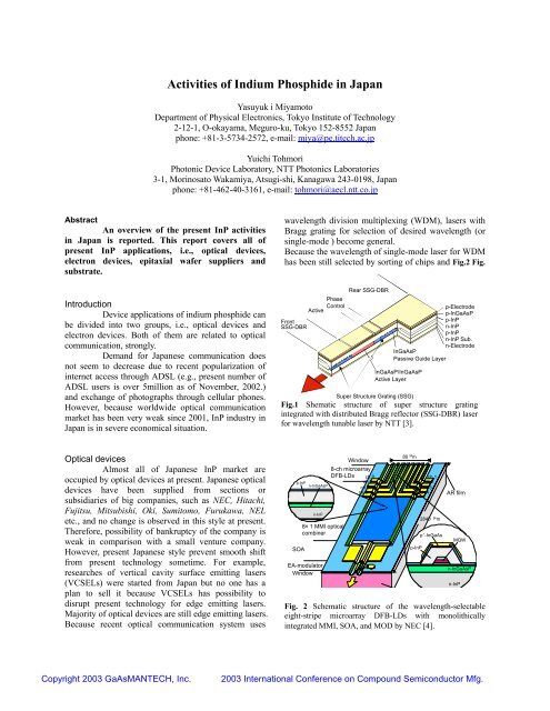
Activities of Indium Phosphide in Japan
Activities of Indium Phosphide in Japan
Activities of Indium Phosphide in Japan

Create successful ePaper yourself
Turn your PDF publications into a flip-book with our unique Google optimized e-Paper software.
<strong>Activities</strong> <strong>of</strong> <strong>Indium</strong> <strong>Phosphide</strong> <strong>in</strong> <strong>Japan</strong><br />
Yasuyuk i Miyamoto<br />
Department <strong>of</strong> Physical Electronics, Tokyo Institute <strong>of</strong> Technology<br />
2-12-1, O-okayama, Meguro-ku, Tokyo 152-8552 <strong>Japan</strong><br />
phone: +81-3-5734-2572, e-mail: miya@pe.titech.ac.jp<br />
Yuichi Tohmori<br />
Photonic Device Laboratory, NTT Photonics Laboratories<br />
3-1, Mor<strong>in</strong>osato Wakamiya, Atsugi-shi, Kanagawa 243-0198, <strong>Japan</strong><br />
phone: +81-462-40-3161, e-mail: tohmori@aecl.ntt.co.jp<br />
Abstract<br />
An overview <strong>of</strong> the present InP activities<br />
<strong>in</strong> <strong>Japan</strong> is reported. This report covers all <strong>of</strong><br />
present InP applications, i.e., optical devices,<br />
electron devices, epitaxial wafer suppliers and<br />
substrate.<br />
Introduction<br />
Device applications <strong>of</strong> <strong>in</strong>dium phosphide can<br />
be divided <strong>in</strong>to two groups, i.e., optical devices and<br />
electron devices. Both <strong>of</strong> them are related to optical<br />
communication, strongly.<br />
Demand for <strong>Japan</strong>ese communication does<br />
not seem to decrease due to recent popularization <strong>of</strong><br />
<strong>in</strong>ternet access through ADSL (e.g., present number <strong>of</strong><br />
ADSL users is over 5million as <strong>of</strong> November, 2002.)<br />
and exchange <strong>of</strong> photographs through cellular phones.<br />
However, because worldwide optical communication<br />
market has been very weak s<strong>in</strong>ce 2001, InP <strong>in</strong>dustry <strong>in</strong><br />
<strong>Japan</strong> is <strong>in</strong> severe economical situation.<br />
wavelength division multiplex<strong>in</strong>g (WDM), lasers with<br />
Bragg grat<strong>in</strong>g for selection <strong>of</strong> desired wavelength (or<br />
s<strong>in</strong>gle-mode ) become general.<br />
Because the wavelength <strong>of</strong> s<strong>in</strong>gle-mode laser for WDM<br />
has been still selected by sort<strong>in</strong>g <strong>of</strong> chips and Fig.2 Fig.<br />
Front<br />
SSG-DBR<br />
Active<br />
Phase<br />
Control<br />
Rear SSG-DBR<br />
Super Structure Grat<strong>in</strong>g (SSG)<br />
p-Electrode<br />
p-InGaAsP<br />
p-InP<br />
n-InP<br />
p-InP<br />
n-InP Sub.<br />
n-Electrode<br />
InGaAsP<br />
Passive Guide Layer<br />
InGaAsP/InGaAsP<br />
Active Layer<br />
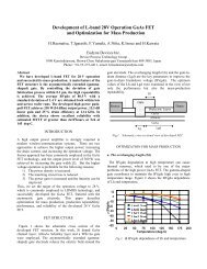
Fig.1 Shematic structure <strong>of</strong> super structure grat<strong>in</strong>g<br />
<strong>in</strong>tegrated with distributed Bragg reflector (SSG-DBR) laser<br />
for wavelength tunable laser by NTT [3].<br />
Optical devices<br />
Almost all <strong>of</strong> <strong>Japan</strong>ese InP market are<br />
occupied by optical devices at present. <strong>Japan</strong>ese optical<br />
devices have been supplied from sections or<br />
subsidiaries <strong>of</strong> big companies, such as NEC, Hitachi,<br />
Fujitsu, Mitsubishi, Oki, Sumitomo, Furukawa, NEL<br />
etc., and no change is observed <strong>in</strong> this style at present.<br />
Therefore, possibility <strong>of</strong> bankruptcy <strong>of</strong> the company is<br />
weak <strong>in</strong> comparison with a small venture company.<br />
However, present <strong>Japan</strong>ese style prevent smooth shift<br />
from present technology sometime. For example,<br />
researches <strong>of</strong> vertical cavity surface emitt<strong>in</strong>g lasers<br />
(VCSELs) were started from <strong>Japan</strong> but no one has a<br />
plan to sell it because VCSELs has possibility to<br />
disrupt present technology for edge emitt<strong>in</strong>g lasers.<br />
Majority <strong>of</strong> optical devices are still edge emitt<strong>in</strong>g lasers.<br />
Because recent optical communication system uses<br />
p-InP<br />
n-InGaAsP<br />
SOA<br />
n-InP<br />
8× 1 MMI optical<br />
comb<strong>in</strong>er<br />
EA-modulator<br />
W<strong>in</strong>dow<br />
W<strong>in</strong>dow<br />
8-ch microarray<br />
DFB-LDs ch.8<br />
ch.7<br />
ch.6<br />
ch.5<br />
80 µ m<br />
p-InP<br />
ch.1<br />
ch.2<br />
ch.3<br />
ch.4<br />
2840 µ m<br />
p + -InGaAs<br />
AR film<br />
MQW<br />
n-InGaAsP<br />
n-InP<br />
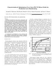
Fig. 2 Schematic structure <strong>of</strong> the wavelength-selectable<br />
eight-stripe microarray DFB-LDs with monolithically<br />
<strong>in</strong>tegrated MMI, SOA, and MOD by NEC [4].
control <strong>of</strong> the operat<strong>in</strong>g temperature, R&D community<br />
for optical devices has an <strong>in</strong>terest <strong>in</strong> development <strong>of</strong><br />
semiconductor tunable lasers. To obta<strong>in</strong> several tens<br />
nanometer as tunable wavelength region, <strong>in</strong>troduction<br />
<strong>of</strong> special Bragg grat<strong>in</strong>g <strong>in</strong>to laser cavity by NTT [3]<br />
and comb<strong>in</strong>ation <strong>of</strong> arrayed lasers with tunable<br />
wavelength range <strong>of</strong> several nanometers by NEC [4]<br />
were reported. Another <strong>in</strong>terest is uncooled laser for<br />
short distance (or Metro) optical communication<br />
system. Lasers modulated at 10 Gb/s up to 85 o C were<br />
developed by <strong>in</strong>sertion <strong>of</strong> potential barrier around<br />
active region by Hitachi [5]. The barrier with<br />
alum<strong>in</strong>um composition prevents carrier overflow at<br />
high temperature.<br />
HR-film<br />
n-electrode<br />
InGaAsP<br />
grat<strong>in</strong>g<br />
p-InP<br />
InGaAlAs-MQW<br />
n-InP<br />
AR-film<br />
n-InP<br />
p-electrode<br />
p-InP<br />
InGaAlAs-MQW<br />
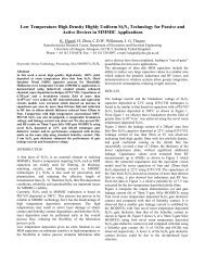
Fig.3 1.3-µm InGaAlAs-MQW DFB laser by Hitachi [5].<br />
Epitaxial wafer suppliers<br />
At present, edge emitt<strong>in</strong>g laser for optical<br />
communication requires crystal regrowth or selective<br />
growth for current conf<strong>in</strong>ement or Bragg grat<strong>in</strong>g. Thus<br />
process such as lithography or etch<strong>in</strong>g is required<br />
before the growth. As a result, the growth is a major<br />
part <strong>of</strong> fabrication process and suppliers cont<strong>in</strong>ue to<br />
grow it themselves. Thus, InP epitaxial wafer suppliers<br />
such as Sumitomo and NTT-AT (subsidiary <strong>of</strong> NTT )<br />
must focus on small market such as wafers for detector<br />
or research.<br />
Electron Devices<br />
Because CMOS can supply very high-scale<br />
<strong>in</strong>tegration circuits with low cost, applications <strong>of</strong><br />
another high-speed electron devices are limited to<br />
high-speed optical transmission system, RF/microwave<br />
transceivers and high-frequency ADCs and DACs [6].<br />
In such fields, present <strong>in</strong>terest <strong>of</strong> <strong>Japan</strong>ese community<br />
for InP electron devices is limited to circuits for<br />
high-speed optical transmission system over 10 Gb/s.<br />
Present target <strong>of</strong> the speed is 40 Gb/s. The circuits for<br />
40Gb/s was reported <strong>in</strong> 1997 already [7]. However,<br />
actual commercial use is delayed due to recent<br />
shr<strong>in</strong>kage <strong>of</strong> optical communication market. Actually,<br />
InP electron device is not commercialized except<br />
devices for measurement system or small sample at<br />
present. SiGe bipolar transistor, present competitor <strong>of</strong><br />
InP electron devices, gets the possibility to reach 40<br />
Gb/s as the system <strong>in</strong> this delay. However, InP electron<br />
devices has <strong>in</strong>herent high-speed <strong>of</strong> electron, thus the<br />
devices must work as major electron electron devices<br />
when the speed is over 40 Gb/s. Recently, 100-Gbit/s<br />
multiplex<strong>in</strong>g and demultiplex<strong>in</strong>g error-free logic<br />
operations was reported [8].<br />
Fig.4 40 Gb/s optical repeater <strong>in</strong> 1997 by NTT [7].<br />
Fig.5 100 Gb/s output waveforms <strong>of</strong> the<br />
selector IC by NTT [8].
Fig.6 Microwave performance <strong>of</strong> fastest InP<br />
HEMT by Fujitsu and CRL [10].<br />
Fig.7 Common-emitter I-V characteristics <strong>of</strong><br />
InP DHBT with highest current density as InP<br />
HBT [13]<br />
The performance <strong>of</strong> <strong>Japan</strong>ese InP electron<br />
device itself is <strong>in</strong> the state <strong>of</strong> the art. Especially, InP<br />
high electron mobility transistors (HEMTs) cont<strong>in</strong>ue to<br />
have highest cut<strong>of</strong>f frequency (f T ) records <strong>in</strong> the world<br />
from 1998. This record was started from f T <strong>of</strong> 350 GHz<br />
by NTT [9]. Present world record is 562 GHz reported<br />
from jo<strong>in</strong>t research team <strong>of</strong> Fujitsu and Communication<br />
Research Laboratories [10]. Delay time <strong>of</strong> 4.6 ps for<br />
logic circuit was also reported by us<strong>in</strong>g r<strong>in</strong>g oscillator<br />
[11].<br />
In other InP electron devices, NTT reported<br />
highest f T <strong>of</strong> 341 GHz <strong>in</strong> heterojunction bipolar<br />
transistors (HBTs) [12]. Highest current density as InP<br />
HBTs was also reported at the same time. Toward low<br />
power dissipation and higher performance <strong>in</strong> the future,<br />
narrowest emitter width [13], smallest total<br />
base-collector capacitance [14] were also reported.<br />
Undoped emitter for high-speed operation by relatively<br />
low current density [15] and simple fabrication process<br />
with sufficient speed and good uniformity [16] were<br />
also reported as another <strong>in</strong>terest<strong>in</strong>g directions.<br />
Substrates<br />
F<strong>in</strong>ally, we would like to comment InP<br />
substrates <strong>in</strong> <strong>Japan</strong>. Two major companies <strong>in</strong> <strong>Japan</strong>,<br />
Sumitomo and Nikko Materals (former <strong>Japan</strong> Energy)<br />
are major suppliers <strong>of</strong> InP substrates <strong>in</strong> the world.<br />
Recently, Showa Denko announces that they can supply<br />
6-<strong>in</strong>ch wafer as a sample [17]. However, <strong>in</strong>tegration <strong>of</strong><br />
optical devices is not progressed except comb<strong>in</strong>ation <strong>of</strong><br />
laser and modulator and demand for larger size <strong>of</strong><br />
substrate is not so high. A 2-<strong>in</strong>ch wafer is majority <strong>in</strong><br />
case <strong>of</strong> optical devices at present. Thus it will take time<br />
to use the larger-size wafer for commercialized<br />
production because we must wait commercialization <strong>of</strong><br />
Fig.8 6” Diameter Fe-doped InP S<strong>in</strong>gle<br />
Crystal by Showa Denko [17]. Right hand side<br />
disc is standard compact disc.<br />
InP electron devices and replacement <strong>of</strong> apparatus for<br />
size-up <strong>of</strong> wafer.<br />
Conclusions<br />
Strong capability <strong>of</strong> InP <strong>in</strong>dustry <strong>in</strong> <strong>Japan</strong> are<br />
demonstrated through research and development <strong>of</strong><br />
new devices and materials. However, recent recession<br />
<strong>of</strong> worldwide optical communication market made a<br />
strong damage <strong>in</strong> the InP <strong>in</strong>dustry <strong>in</strong> <strong>Japan</strong>, because<br />
present InP applications <strong>in</strong> <strong>Japan</strong> is limited to optical<br />
communication area.<br />
Acknowledgements<br />
We appreciate Drs. K. Kudo, M. Aoki, T.<br />
Enoki, A. Endoh and K. Sh<strong>in</strong>ohara for discussion and<br />
provid<strong>in</strong>g the data. A Part <strong>of</strong> this work was supported<br />
by the M<strong>in</strong>istry <strong>of</strong> Education, Science, Culture and<br />
Sports through a Scientific Grant-In-Aid, <strong>Japan</strong><br />
Science and Technology Corporation through CRAEST
and the M<strong>in</strong>istry <strong>of</strong> Public Management, Public Affairs,<br />
Posts and Telecommunications through the Grant for<br />
“Development <strong>of</strong> Frequency Resources”.<br />
References<br />
[1] K. Okubo, 7th Opto-Electronics and<br />
Communications Conference, Plenary Talk -2,<br />
Kanagawa, <strong>Japan</strong>, July 2002.<br />
[2] K. Iga, 59th Device Research Conference, L-2,<br />
Notre Dame, IN June 2001.<br />
[3] Y. Tohmori, Y. Yoshikuni, H. Ishii, F. Kano, T.<br />
Tamamura, and Y. Kondo, Electron. Lett., vol.29,<br />
pp.352-353, 1993.<br />
[4] K. Kudo, K. Yashiki, T. Sasaki, Y. Yokoyama, K.<br />
Hashimoto, T. Takao, and M. Yamaguchi, IEEE<br />
Photon. Tech. Lett., vol12, pp.242-244, 2000.<br />
[5] M. Aoki, T. Sudo, T. Tsuchiya, D. Takemoto, and<br />
S. Tsuji, Proc. ECOC 2000, vol.1. pp123-124,<br />
2000.<br />
[6] M.J.W Rodwel, D. Scott, M. Urteaga, D.<br />
Dahlstorm, S. Krishnan, Z. Grififth, Y. Wei., N.<br />
Parthasarathy, and Y-M Kim, 2002 Int. Conf.<br />
on Solid State Devices and Materials, E1-1,<br />
Nagoya, <strong>Japan</strong>, Sept. 2002.<br />
[7] M. Yoneyama, A. Sano, K. Hagimoto, T. Otsuji,<br />
K. Murata, Y. Imai, S. Yamaguchi, T. Enoki and<br />
E.Sano, IEEE Tran. IEEE Trans. Microwave<br />
Theory Tech., vol.45, no.12, pp.2274-2282,<br />
1997.<br />
[8] K. Murata, K. Sano, H. Kitabayashi, S. Sugitani,<br />
H. Sugahara and T. Enoki, IEEE Int. Electron<br />
Device Meetng Tech.Dig., San Francisco, 2002.<br />
[9] T. Suemitsu, T. Enoki, H. Yokoyama, Y. Umeda,<br />
T. Enoki, Y. Ishii and T.Tamamura: IEEE Int.<br />
Electron Device Meetng Tech.Dig., San<br />
Francisco, 1998, p. 223.<br />
[10] A. Endoh, Y. Yamashita, K. Sh<strong>in</strong>ohara, K.<br />
Hikosaka, T. Matsui, S. Hiyamizu and T.<br />
Mimura, 2002 Int. Conf. on Solid State<br />
Devices and Materials, G1-3, Nagoya, <strong>Japan</strong>,<br />
Sept. 2002.<br />
[11] Y. Umeda, K. Osafune, T. Enoki, H. Yokoyama<br />
and Y. Ishii: IEEE MTT-S Int. Microwave Symp.<br />
Dig., Anaheim, 1999, p. 205.<br />
[12] M. Ida, K. Kurishima, and N. Watanabe:IEEE<br />
Electron Dev. Lett.., vol.23, no.12, 2002.<br />
[13] Y. Miyamoto, T. Arai, S. Yamagami, K. Matsuda,<br />
K. Furuya, 2002 Int. Conf. on Solid State<br />
Devices and Materials, E1-4, Nagoya, <strong>Japan</strong>,<br />
Sept. 2002,<br />
[14] T. Morita,T. Arai,H. Nagatsuka,Y. Miyamoto,K.<br />
Furuya, Jpn. J. Appl. Phys., vol.41, no.2A<br />
pp.L121 - L123, 2002.<br />
[15] M. Ida, K. Kurishima, H. Nakajima, N.<br />
Watanabe, and S. Yamahata: IEEE Int. Electron<br />
Device Meetng Tech.Dig., San Francisco, 2000,<br />
p.854.<br />
[16] K. Kotani, R. Yamabi, T. Kawasaki, M.<br />
Yanagisawa, S. Yaegassi and H. Yano, 2002 Int.<br />
Conf. on Solid State Devices and Materials, E1-5,<br />
Nagoya, <strong>Japan</strong>, Sept. 2002.<br />
[17] http://www.sdk.co.jp/enews/news02/02-04-<br />
03.htm