SD Specifications Part 1 Physical Layer Simplified Specification
SD Specifications Part 1 Physical Layer Simplified Specification
SD Specifications Part 1 Physical Layer Simplified Specification

You also want an ePaper? Increase the reach of your titles
YUMPU automatically turns print PDFs into web optimized ePapers that Google loves.
<strong>SD</strong> <strong><strong>Specification</strong>s</strong><br />
<strong>Part</strong> 1<br />
<strong>Physical</strong> <strong>Layer</strong><br />
<strong>Simplified</strong> <strong>Specification</strong><br />
Version 3.01<br />
May 18, 2010<br />
<strong>SD</strong> Group<br />
Panasonic Corporation<br />
SanDisk Corporation<br />
Toshiba Corporation<br />
Technical Committee<br />
<strong>SD</strong> Card Association
©Copyright 2001-2010 <strong>SD</strong> Group (Panasonic, SanDisk, Toshiba) and <strong>SD</strong> Card Association<br />
<strong>Physical</strong> <strong>Layer</strong> <strong>Simplified</strong> <strong>Specification</strong> Version 3.01<br />
Revision History<br />
Date Version Changes compared to previous issue<br />
April 3, 2006 1.10 <strong>Physical</strong> <strong>Layer</strong> <strong>Simplified</strong> <strong>Specification</strong> Version 1.10 initial release.<br />
(Supplementary Notes Ver1.00 is applied.)<br />
September 25, 2006 2.00 <strong>Physical</strong> <strong>Layer</strong> <strong>Simplified</strong> <strong>Specification</strong> Version 2.00<br />
May 18, 2010 3.01 <strong>Physical</strong> <strong>Layer</strong> <strong>Simplified</strong> <strong>Specification</strong> Version 3.01<br />
To the extent this proposed specification, which is being submitted for review under the IP<br />
Policy, implements, incorporates by reference or refers to any portion of versions 1.0 or 1.01<br />
of the <strong>SD</strong> <strong><strong>Specification</strong>s</strong> (including <strong>Part</strong>s 1 through 4), adoption of the proposed specification<br />
shall require Members utilizing the adopted specification to obtain the appropriate licenses<br />
from the <strong>SD</strong>-3C, LLC, as required for the utilization of those portion(s) of versions 1.0 or 1.01<br />
of the <strong>SD</strong> <strong><strong>Specification</strong>s</strong>.<br />
For example, implementation of the <strong>SD</strong> <strong><strong>Specification</strong>s</strong> in a host device under versions 1.0 or<br />
1.01 and under the adopted specification requires the execution of a <strong>SD</strong> Host Ancillary<br />
License Agreement with the <strong>SD</strong>-3C, LLC; and implementation of the <strong>SD</strong> <strong><strong>Specification</strong>s</strong> under<br />
versions 1.0 or 1.01 and under the proposed specification in a <strong>SD</strong> Card containing any<br />
memory storage capability (other than for storage of executable code for a controller or<br />
microprocessor within the <strong>SD</strong> Card) requires the execution of a <strong>SD</strong> Memory Card License<br />
Agreement with the <strong>SD</strong>-3C, LLC.<br />
i
©Copyright 2001-2010 <strong>SD</strong> Group (Panasonic, SanDisk, Toshiba) and <strong>SD</strong> Card Association<br />
<strong>Physical</strong> <strong>Layer</strong> <strong>Simplified</strong> <strong>Specification</strong> Version 3.01<br />
Conditions for publication<br />
Publisher:<br />
<strong>SD</strong> Card Association<br />
2400 Camino Ramon, Suite 375<br />
San Ramon, CA 94583 USA<br />
Telephone: +1 (925) 275-6615,<br />
Fax: +1 (925) 886-4870<br />
E-mail: office@sdcard.org<br />
Copyright Holders:<br />
The <strong>SD</strong> Group<br />
Panasonic Corporation<br />
SanDisk Corporation<br />
Toshiba Corporation<br />
The <strong>SD</strong> Card Association<br />
Notes:<br />
The copyright of the previous versions (Version 1.00 and 1.01) and all corrections or non-material<br />
changes thereto are owned by <strong>SD</strong> Group.<br />
The copyright of material changes to the previous versions (Version 1.01) are owned by <strong>SD</strong> Card<br />
Association.<br />
Disclaimers:<br />
The information contained herein is presented only as a standard specification for <strong>SD</strong> Card and <strong>SD</strong><br />
Host/Ancillary products. No responsibility is assumed by <strong>SD</strong> Card Association for any damages, any<br />
infringements of patents or other right of the third parties, which may result from its use. No license is<br />
granted by implication or otherwise under any patent or rights of <strong>SD</strong> Group and <strong>SD</strong> Card Association or<br />
others.<br />
ii
©Copyright 2001-2010 <strong>SD</strong> Group (Panasonic, SanDisk, Toshiba) and <strong>SD</strong> Card Association<br />
<strong>Physical</strong> <strong>Layer</strong> <strong>Simplified</strong> <strong>Specification</strong> Version 3.01<br />
Conventions Used in This Document<br />
Naming Conventions<br />
• Some terms are capitalized to distinguish their definition from their common English meaning. Words<br />
not capitalized have their common English meaning.<br />
Numbers and Number Bases<br />
• Hexadecimal numbers are written with a lower case "h" suffix, e.g., FFFFh and 80h.<br />
• Binary numbers are written with a lower case "b" suffix (e.g., 10b).<br />
• Binary numbers larger than four digits are written with a space dividing each group of four digits, as in<br />
1000 0101 0010b.<br />
• All other numbers are decimal.<br />
Key Words<br />
• May: Indicates flexibility of choice with no implied recommendation or requirement.<br />
• Shall: Indicates a mandatory requirement. Designers shall implement such mandatory<br />
requirements to ensure interchangeability and to claim conformance with the specification.<br />
• Should: Indicates a strong recommendation but not a mandatory requirement. Designers should<br />
give strong consideration to such recommendations, but there is still a choice in<br />
implementation.<br />
Application Notes<br />
Some sections of this document provide guidance to the host implementers as follows:<br />
Application Note:<br />
This is an example of an application note.<br />
iii
©Copyright 2001-2010 <strong>SD</strong> Group (Panasonic, SanDisk, Toshiba) and <strong>SD</strong> Card Association<br />
<strong>Physical</strong> <strong>Layer</strong> <strong>Simplified</strong> <strong>Specification</strong> Version 3.01<br />
Table of Contents<br />
1. General Description............................................................................................................1<br />
2. System Features .................................................................................................................3<br />
3. <strong>SD</strong> Memory Card System Concept....................................................................................5<br />
3.1 Read-Write Property......................................................................................................................5<br />
3.2 Supply Voltage...............................................................................................................................5<br />
3.3 Card Capacity................................................................................................................................5<br />
3.3.1 User Area and Protected Area ................................................................................................5<br />
3.3.2 Card Capacity Classification ...................................................................................................5<br />
3.4 Speed Class ..................................................................................................................................6<br />
3.5 Bus Topology .................................................................................................................................6<br />
3.6 Bus Protocol ..................................................................................................................................7<br />
3.6.1 <strong>SD</strong> Bus....................................................................................................................................7<br />
3.6.2 SPI Bus .................................................................................................................................10<br />
3.7 <strong>SD</strong> Memory Card–Pins and Registers......................................................................................... 11<br />
3.8 ROM Card ................................................................................................................................... 11<br />
3.8.1 Register Setting Requirements .............................................................................................11<br />
3.8.2 Unsupported Commands ......................................................................................................11<br />
3.8.3 Optional Commands ............................................................................................................. 11<br />
3.8.4 WP Switch.............................................................................................................................12<br />
3.9 Ultra High Speed Phase I (UHS-I) Card ......................................................................................13<br />
3.9.1 UHS-I Operation Modes........................................................................................................13<br />
3.9.2 UHS-I Card Types .................................................................................................................13<br />
3.9.3 Host and Card Combination..................................................................................................14<br />
3.9.4 Bus Speed Modes Selection Sequence................................................................................15<br />
3.9.5 UHS System Block Diagram .................................................................................................16<br />
3.9.6 Summary of Bus Speed Mode ..............................................................................................17<br />
4. <strong>SD</strong> Memory Card Functional Description .......................................................................18<br />
4.1 General........................................................................................................................................18<br />
4.2 Card Identification Mode..............................................................................................................19<br />
4.2.1 Card Reset............................................................................................................................19<br />
4.2.2 Operating Condition Validation..............................................................................................19<br />
4.2.3 Card Initialization and Identification Process ........................................................................21<br />
4.2.3.1 Initialization Command (ACMD41)........................................................................................ 23<br />
4.2.4 Bus Signal Voltage Switch Sequence ...................................................................................24<br />
4.2.4.1 Initialization Sequence for UHS-I .......................................................................................... 24<br />
4.2.4.2 Timing to Switch Signal Voltage............................................................................................ 25<br />
4.2.4.3 Timing of Voltage Switch Error Detection.............................................................................. 25<br />
4.2.4.4 Voltage Switch Command..................................................................................................... 25<br />
4.2.4.5 Tuning Command ................................................................................................................. 25<br />
4.2.4.6 An Example of UHS-I System Block Diagram....................................................................... 26<br />
4.3 Data Transfer Mode.....................................................................................................................27<br />
4.3.1 Wide Bus Selection/Deselection ...........................................................................................29<br />
4.3.2 2 GByte Card ........................................................................................................................29<br />
iv
©Copyright 2001-2010 <strong>SD</strong> Group (Panasonic, SanDisk, Toshiba) and <strong>SD</strong> Card Association<br />
<strong>Physical</strong> <strong>Layer</strong> <strong>Simplified</strong> <strong>Specification</strong> Version 3.01<br />
4.3.3 Data Read .............................................................................................................................29<br />
4.3.4 Data Write .............................................................................................................................30<br />
4.3.5 Erase.....................................................................................................................................32<br />
4.3.6 Write Protect Management ...................................................................................................32<br />
4.3.7 Card Lock/Unlock Operation .................................................................................................33<br />
4.3.7.1 General................................................................................................................................. 33<br />
4.3.7.2 Parameter and the Result of CMD42.................................................................................... 35<br />
4.3.7.3 Forcing Erase ....................................................................................................................... 37<br />
4.3.7.3.1 Force Erase Function to the Locked Card...................................................................... 37<br />
4.3.7.4 Relation Between ACMD6 and Lock/Unlock State................................................................ 38<br />
4.3.7.5 Commands Accepted for Locked Card ................................................................................. 38<br />
4.3.7.6 Two Types of Lock/Unlock Card............................................................................................ 39<br />
4.3.8 Content Protection ................................................................................................................39<br />
4.3.9 Application-Specific Commands............................................................................................40<br />
4.3.9.1 Application-Specific Command – APP_CMD (CMD55)......................................................... 40<br />
4.3.9.2 General Command - GEN_CMD (CMD56)........................................................................... 40<br />
4.3.10 Switch Function Command .................................................................................................41<br />
4.3.10.1 General............................................................................................................................... 41<br />
4.3.10.2 Mode 0 Operation - Check Function ................................................................................... 43<br />
4.3.10.3 Mode 1 Operation - Set Function........................................................................................43<br />
4.3.10.4 Switch Function Status........................................................................................................ 46<br />
4.3.10.4.1 Busy Status Indication for Functions ............................................................................ 47<br />
4.3.10.4.2 Data Structure Version ................................................................................................. 48<br />
4.3.10.4.3 Function Table of Switch Command ............................................................................. 48<br />
4.3.10.5 Relationship between CMD6 data & other commands ....................................................... 49<br />
4.3.10.6 Switch Function Flow Example ...........................................................................................49<br />
4.3.10.7 Example of Checking.......................................................................................................... 49<br />
4.3.11 High-Speed Mode (25 MB/sec interface speed)..................................................................50<br />
4.3.12 Command System...............................................................................................................50<br />
4.3.13 Send Interface Condition Command (CMD8) .....................................................................51<br />
4.3.14 Command Functional Difference in Card Capacity Types...................................................52<br />
4.4 Clock Control ...............................................................................................................................53<br />
4.5 Cyclic Redundancy Code (CRC) .................................................................................................54<br />
4.6 Error Conditions...........................................................................................................................56<br />
4.6.1 CRC and Illegal Command ...................................................................................................56<br />
4.6.2 Read, Write and Erase Timeout Conditions ..........................................................................56<br />
4.6.2.1 Read ..................................................................................................................................... 56<br />
4.6.2.2 Write ..................................................................................................................................... 56<br />
4.6.2.3 Erase .................................................................................................................................... 57<br />
4.7 Commands ..................................................................................................................................58<br />
4.7.1 Command Types ...................................................................................................................58<br />
4.7.2 Command Format .................................................................................................................58<br />
4.7.3 Command Classes................................................................................................................58<br />
4.7.4 Detailed Command Description ............................................................................................61<br />
4.8 Card State Transition Table .........................................................................................................69<br />
4.9 Responses...................................................................................................................................71<br />
4.9.1 R1 (normal response command):..........................................................................................71<br />
4.9.2 R1b........................................................................................................................................71<br />
4.9.3 R2 (CID, C<strong>SD</strong> register) .........................................................................................................71<br />
4.9.4 R3 (OCR register) .................................................................................................................72<br />
4.9.5 R6 (Published RCA response) ..............................................................................................72<br />
4.9.6 R7 (Card interface condition) ................................................................................................73<br />
v
©Copyright 2001-2010 <strong>SD</strong> Group (Panasonic, SanDisk, Toshiba) and <strong>SD</strong> Card Association<br />
<strong>Physical</strong> <strong>Layer</strong> <strong>Simplified</strong> <strong>Specification</strong> Version 3.01<br />
4.10 Two Status Information of <strong>SD</strong> Memory Card .............................................................................74<br />
4.10.1 Card Status .........................................................................................................................74<br />
4.10.2 <strong>SD</strong> Status ............................................................................................................................78<br />
4.11 Memory Array <strong>Part</strong>itioning .........................................................................................................82<br />
4.12 Timings ......................................................................................................................................82<br />
4.13 Speed Class <strong>Specification</strong> .........................................................................................................83<br />
4.13.1 Speed Class <strong>Specification</strong> for <strong>SD</strong>SC and <strong>SD</strong>HC ................................................................83<br />
4.13.1.1 Allocation Unit (AU)............................................................................................................. 83<br />
4.13.1.2 Recording Unit (RU) ........................................................................................................... 83<br />
4.13.1.3 Write Performance.............................................................................................................. 84<br />
4.13.1.4 Read Performance.............................................................................................................. 84<br />
4.13.1.5 Performance Curve Definition............................................................................................. 84<br />
4.13.1.6 Speed Class Definition........................................................................................................ 84<br />
4.13.1.7 Consideration for Inserting FAT Update during Recording.................................................. 85<br />
4.13.1.8 Measurement Conditions and Requirements of the Speed Class....................................... 85<br />
4.13.2 Speed Class <strong>Specification</strong> for <strong>SD</strong>XC...................................................................................86<br />
4.13.2.1 Speed Class Parameters .................................................................................................... 86<br />
4.13.2.1.1 AU ................................................................................................................................ 86<br />
4.13.2.1.2 RU................................................................................................................................ 86<br />
4.13.2.2 Write Performance.............................................................................................................. 86<br />
4.13.2.3 Read Performance.............................................................................................................. 86<br />
4.13.2.4 FAT Update......................................................................................................................... 86<br />
4.13.2.5 CI (Continuous Information) Update ................................................................................... 86<br />
4.13.2.6 Distinction of Data Type ...................................................................................................... 86<br />
4.13.2.7 Measurement Conditions and Requirements of the Speed Class for <strong>SD</strong>XC....................... 86<br />
4.13.2.8 Speed Class Control Command (CMD20) .......................................................................... 87<br />
4.13.3 Speed Grade <strong>Specification</strong> for UHS-I..................................................................................87<br />
4.13.4 Notes for Preparation Time of UHS-I Card..........................................................................87<br />
4.14 Erase Timeout Calculation.........................................................................................................88<br />
4.14.1 Erase Unit ...........................................................................................................................88<br />
4.14.2 Case Analysis of Erase Time Characteristics......................................................................88<br />
4.14.3 Method for Erase Large Areas ............................................................................................89<br />
4.14.4 Calculation of Erase Timeout Value Using the Parameter Registers ..................................89<br />
4.14.5 Set Block Count Command.................................................................................................90<br />
5. Card Registers ..................................................................................................................91<br />
5.1 OCR register................................................................................................................................92<br />
5.2 CID register .................................................................................................................................93<br />
5.3 C<strong>SD</strong> Register...............................................................................................................................95<br />
5.3.1 C<strong>SD</strong>_STRUCTURE ..............................................................................................................95<br />
5.3.2 C<strong>SD</strong> Register (C<strong>SD</strong> Version 1.0) ..........................................................................................96<br />
5.3.3 C<strong>SD</strong> Register (C<strong>SD</strong> Version 2.0) ........................................................................................103<br />
5.4 RCA register ..............................................................................................................................106<br />
5.5 DSR register (Optional) .............................................................................................................106<br />
5.6 SCR register ..............................................................................................................................106<br />
6. <strong>SD</strong> Memory Card Hardware Interface............................................................................110<br />
6.1 Hot Insertion and Removal ........................................................................................................ 110<br />
6.2 Card Detection (Insertion/Removal) ..........................................................................................110<br />
6.3 Power Protection (Insertion/Removal)....................................................................................... 110<br />
6.4 Power Scheme .......................................................................................................................... 110<br />
6.4.1 Power Up ............................................................................................................................ 110<br />
vi
©Copyright 2001-2010 <strong>SD</strong> Group (Panasonic, SanDisk, Toshiba) and <strong>SD</strong> Card Association<br />
<strong>Physical</strong> <strong>Layer</strong> <strong>Simplified</strong> <strong>Specification</strong> Version 3.01<br />
6.4.1.1 Power Up Time ....................................................................................................................111<br />
6.4.1.2 Power On or Power Cycle....................................................................................................111<br />
6.4.1.3 Power Supply Ramp Up.......................................................................................................111<br />
6.4.2 Power Down and Power Cycle............................................................................................ 112<br />
6.5 Programmable Card Output Driver (Optional) ........................................................................... 112<br />
6.6 Bus Operating Conditions for 3.3V Signaling ............................................................................ 112<br />
6.7 Driver Strength and Bus Timing for 1.8V Signaling ................................................................... 112<br />
6.8 Electrical Static Discharge (E<strong>SD</strong>) Requirement......................................................................... 112<br />
7. SPI Mode..........................................................................................................................113<br />
7.1 Introduction................................................................................................................................ 113<br />
7.2 SPI Bus Protocol ....................................................................................................................... 113<br />
7.2.1 Mode Selection and Initialization.........................................................................................114<br />
7.2.2 Bus Transfer Protection....................................................................................................... 116<br />
7.2.3 Data Read ........................................................................................................................... 116<br />
7.2.4 Data Write ........................................................................................................................... 117<br />
7.2.5 Erase & Write Protect Management.................................................................................... 118<br />
7.2.6 Read CID/C<strong>SD</strong> Registers....................................................................................................119<br />
7.2.7 Reset Sequence.................................................................................................................. 119<br />
7.2.8 Error Conditions .................................................................................................................. 119<br />
7.2.9 Memory Array <strong>Part</strong>itioning................................................................................................... 119<br />
7.2.10 Card Lock/Unlock.............................................................................................................. 119<br />
7.2.11 Application Specific Commands ........................................................................................ 119<br />
7.2.12 Content Protection Command...........................................................................................120<br />
7.2.13 Switch Function Command ...............................................................................................120<br />
7.2.14 High Speed Mode..............................................................................................................120<br />
7.2.15 Speed Class <strong>Specification</strong>.................................................................................................120<br />
7.3 SPI Mode Transaction Packets .................................................................................................121<br />
7.3.1 Command Tokens ...............................................................................................................121<br />
7.3.1.1 Command Format............................................................................................................... 121<br />
7.3.1.2 Command Classes ............................................................................................................. 121<br />
7.3.1.3 Detailed Command Description .......................................................................................... 123<br />
7.3.1.4 Card Operation for CMD8 in SPI mode .............................................................................. 128<br />
7.3.2 Responses ..........................................................................................................................129<br />
7.3.2.1 Format R1........................................................................................................................... 129<br />
7.3.2.2 Format R1b......................................................................................................................... 129<br />
7.3.2.3 Format R2........................................................................................................................... 130<br />
7.3.2.4 Format R3........................................................................................................................... 131<br />
7.3.2.5 Formats R4 & R5 ................................................................................................................ 131<br />
7.3.2.6 Format R7........................................................................................................................... 131<br />
7.3.3 Control Tokens ....................................................................................................................132<br />
7.3.3.1 Data Response Token......................................................................................................... 132<br />
7.3.3.2 Start Block Tokens and Stop Tran Token............................................................................. 132<br />
7.3.3.3 Data Error Token................................................................................................................. 133<br />
7.3.4 Clearing Status Bits.............................................................................................................133<br />
7.4 Card Registers...........................................................................................................................134<br />
7.5 SPI Bus Timing Diagrams..........................................................................................................134<br />
7.6 SPI Electrical Interface ..............................................................................................................135<br />
7.7 SPI Bus Operating Conditions...................................................................................................135<br />
7.8 Bus Timing.................................................................................................................................135<br />
Appendix A (Normative) : Reference.................................................................................136<br />
vii
©Copyright 2001-2010 <strong>SD</strong> Group (Panasonic, SanDisk, Toshiba) and <strong>SD</strong> Card Association<br />
<strong>Physical</strong> <strong>Layer</strong> <strong>Simplified</strong> <strong>Specification</strong> Version 3.01<br />
A.1 Related Documentation.............................................................................................................136<br />
Appendix B (Normative) : Special Terms..........................................................................137<br />
B.1 Terminology...............................................................................................................................137<br />
B.2 Abbreviations.............................................................................................................................137<br />
Appendix C (Informative) : Examples for Fixed Delay UHS-I Host Design ...................139<br />
Appendix D : UHS-I Tuning Procedure..............................................................................140<br />
Appendix E : Host Design Recommendation ...................................................................141<br />
viii
©Copyright 2001-2010 <strong>SD</strong> Group (Panasonic, SanDisk, Toshiba) and <strong>SD</strong> Card Association<br />
<strong>Physical</strong> <strong>Layer</strong> <strong>Simplified</strong> <strong>Specification</strong> Version 3.01<br />
Table of Figures<br />
Figure 1-1: <strong>SD</strong> <strong><strong>Specification</strong>s</strong> Documentation Structure................................................................................ 1<br />
Figure 3-1: "no response" and "no data" Operations ..................................................................................... 7<br />
Figure 3-2: (Multiple) Block Read Operation ................................................................................................. 7<br />
Figure 3-3: (Multiple) Block Write Operation.................................................................................................. 8<br />
Figure 3-4: Command Token Format............................................................................................................. 8<br />
Figure 3-5: Response Token Format ............................................................................................................. 8<br />
Figure 3-6: Data Packet Format - Usual Data ............................................................................................... 9<br />
Figure 3-7: Data Packet Format - Wide Width Data .................................................................................... 10<br />
Figure 3-8 : UHS-I Card Type Modes of Operation versus Frequency Range............................................. 13<br />
Figure 3-9 : UHS-I Card Type Modes of Operation versus Throughput....................................................... 14<br />
Figure 3-10 : Command Sequence to Use UHS-I ....................................................................................... 15<br />
Figure 4-1: <strong>SD</strong> Memory Card State Diagram (card identification mode)...................................................... 20<br />
Figure 4-2: Card Initialization and Identification Flow (<strong>SD</strong> mode)................................................................ 22<br />
Figure 4-3 : Argument of ACMD41 .............................................................................................................. 23<br />
Figure 4-4 : Response of ACMD41.............................................................................................................. 23<br />
Figure 4-5 : ACMD41 Timing Followed by Voltage Switch Sequence.......................................................... 24<br />
Figure 4-6 : UHS-I Host Initialization Flow Chart ......................................................................................... 24<br />
Figure 4-7 : Voltage Switch Command ........................................................................................................ 25<br />
Figure 4-8 : Send Tuning Block Command.................................................................................................. 26<br />
Figure 4-9: <strong>SD</strong> Memory Card State Diagram (data transfer mode).............................................................. 27<br />
Figure 4-10: Use of Switch Command......................................................................................................... 42<br />
Figure 4-11: Busy Status of 'Command System'.......................................................................................... 47<br />
Figure 4-12: CRC7 Generator/Checker....................................................................................................... 54<br />
Figure 4-13: CRC16 Generator/Checker..................................................................................................... 55<br />
Figure 4-14: Overview of Speed Class <strong>Specification</strong> ................................................................................... 83<br />
Figure 4-15: Definition of Allocation Unit (AU) ............................................................................................. 83<br />
Figure 4-16: Three Performance Curves ..................................................................................................... 85<br />
Figure 4-17: Example Erase Characteristics (Case 1 T OFFSET =0)................................................................ 88<br />
Figure 4-18: Example Erase Characteristics (Case 2 T OFFSET =2)................................................................ 89<br />
Figure 4-19 : Set Block Count Command.................................................................................................... 90<br />
Figure 5-1: ERASE_BLK_EN = 0 Example ............................................................................................... 100<br />
Figure 5-2: ERASE_BLK_EN = 1 Example ............................................................................................... 100<br />
Figure 6-1: Power-up Diagram ...................................................................................................................110<br />
Figure 6-2 : Change of Figure for Power Up..............................................................................................111<br />
Figure 7-1 : <strong>SD</strong> Memory Card State Diagram (SPI mode)..........................................................................114<br />
Figure 7-2: SPI Mode Initialization Flow .....................................................................................................115<br />
Figure 7-3: Single Block Read Operation ...................................................................................................116<br />
Figure 7-4: Read Operation - Data Error ....................................................................................................117<br />
Figure 7-5: Multiple Block Read Operation.................................................................................................117<br />
Figure 7-6: Single Block Write Operation ...................................................................................................117<br />
Figure 7-7: Multiple Block Write Operation .................................................................................................118<br />
Figure 7-8: 'No data' Operations.................................................................................................................118<br />
Figure 7-9: R1 Response Format .............................................................................................................. 129<br />
Figure 7-10: R2 Response Format ............................................................................................................ 130<br />
Figure 7-11: R3 Response Format ............................................................................................................ 131<br />
Figure 7-12: R7 Response Format ............................................................................................................ 131<br />
Figure 7-13: Data Error Token ................................................................................................................... 133<br />
ix
©Copyright 2001-2010 <strong>SD</strong> Group (Panasonic, SanDisk, Toshiba) and <strong>SD</strong> Card Association<br />
<strong>Physical</strong> <strong>Layer</strong> <strong>Simplified</strong> <strong>Specification</strong> Version 3.01<br />
Table of Tables<br />
Table 3-1: <strong>SD</strong> Memory Card Registers.........................................................................................................11<br />
Table 3-2 : Register Setting Requirements for ROM Card............................................................................11<br />
Table 3-3 : Host and Card Combinations..................................................................................................... 14<br />
Table 3-4 : Bus Speed Modes...................................................................................................................... 17<br />
Table 3-5 : Bus Speed Mode Option / Mandatory ........................................................................................ 17<br />
Table 4-1: Overview of Card States vs. Operation Modes ........................................................................... 18<br />
This section is a blank for the <strong>Simplified</strong> <strong>Specification</strong>. ............................................................................... 25<br />
This section is a blank for the <strong>Simplified</strong> <strong>Specification</strong>. ............................................................................... 25<br />
Table 4-2 : Tuning Block Pattern.................................................................................................................. 26<br />
Table 4-3: Read Command Blocklen ........................................................................................................... 30<br />
Table 4-4: Write Command Blocklen ........................................................................................................... 30<br />
Table 4-5: Lock Card Data Structure ........................................................................................................... 33<br />
Table 4-6: Lock Unlock Function (Basic Sequence for CMD42) .................................................................. 36<br />
Table 4-7: Force Erase Function to the Locked Card (Relation to the Write Protects)................................. 37<br />
Table 4-8: Relation between ACMD6 and the Lock/Unlock State ................................................................ 38<br />
Table 4-9: Version Difference of Lock/Unlock Functions.............................................................................. 39<br />
Table 4-10: Available Functions................................................................................................................... 44<br />
Table 4-11: Status Data Structure ................................................................................................................ 47<br />
Table 4-12: Data Structure Version.............................................................................................................. 48<br />
Table 4-13: Status Code of Mode 0 to Supported Function Group .............................................................. 48<br />
Table 4-14: Status Code of Mode 1 to Supported Function Group .............................................................. 49<br />
Table 4-15: Status Code of Mode 0 and 1 to Unsupported Function Group ................................................ 49<br />
Table 4-16: Format of CMD8 ....................................................................................................................... 51<br />
Table 4-17: Command Format..................................................................................................................... 58<br />
Table 4-18: Card Command Classes (CCCs) in <strong>SD</strong> Mode .......................................................................... 60<br />
Table 4-19: Basic Commands (class 0) ....................................................................................................... 62<br />
Table 4-20: Block-Oriented Read Commands (class 2)............................................................................... 63<br />
Table 4-21: Block-Oriented Write Commands (class 4)............................................................................... 63<br />
Table 4-22: Block Oriented Write Protection Commands (class 6) .............................................................. 64<br />
Table 4-23: Erase Commands (class 5) ...................................................................................................... 64<br />
Table 4-24: Lock Card (class 7)................................................................................................................... 65<br />
Table 4-25: Application-Specific Commands (class 8) ................................................................................. 65<br />
Table 4-26: I/O Mode Commands (class 9) ................................................................................................. 65<br />
Table 4-27: Application Specific Commands used/reserved by <strong>SD</strong> Memory Card....................................... 67<br />
Table 4-28: Switch Function Commands (class 10)..................................................................................... 68<br />
Table 4-29: Card State Transition Table....................................................................................................... 70<br />
Table 4-30: Response R1............................................................................................................................ 71<br />
Table 4-31: Response R2............................................................................................................................ 71<br />
Table 4-32: Response R3............................................................................................................................ 72<br />
Table 4-33: Response R6............................................................................................................................ 72<br />
Table 4-34: Response R7............................................................................................................................ 73<br />
Table 4-35: Voltage Accepted in R7............................................................................................................. 73<br />
Table 4-36: Card Status............................................................................................................................... 76<br />
Table 4-37: Card Status Field/Command - Cross Reference....................................................................... 77<br />
Table 4-38: <strong>SD</strong> Status................................................................................................................................. 78<br />
Table 4-39: Speed Class Code Field ........................................................................................................... 79<br />
Table 4-40: Performance Move Field........................................................................................................... 79<br />
Table 4-41: AU_SIZE Field .......................................................................................................................... 80<br />
Table 4-42: Maximum AU size ..................................................................................................................... 80<br />
Table 4-43: Erase Size Field........................................................................................................................ 80<br />
x
©Copyright 2001-2010 <strong>SD</strong> Group (Panasonic, SanDisk, Toshiba) and <strong>SD</strong> Card Association<br />
<strong>Physical</strong> <strong>Layer</strong> <strong>Simplified</strong> <strong>Specification</strong> Version 3.01<br />
Table 4-44: Erase Timeout Field.................................................................................................................. 81<br />
Table 4-45: Erase Offset Field ..................................................................................................................... 81<br />
Table 4-46: UHS_ SPEED_GRADE Field.................................................................................................... 82<br />
Table 4-47: UHS_AU_SIZE Field ................................................................................................................ 82<br />
Table 5-1: OCR Register Definition ............................................................................................................. 92<br />
Table 5-2: The CID Fields............................................................................................................................ 93<br />
Table 5-3: C<strong>SD</strong> Register Structure .............................................................................................................. 95<br />
Table 5-4: The C<strong>SD</strong> Register Fields (C<strong>SD</strong> Version 1.0) .............................................................................. 96<br />
Table 5-5: TAAC Access Time Definition ..................................................................................................... 97<br />
Table 5-6: Maximum Data Transfer Rate Definition ..................................................................................... 97<br />
Table 5-7: Supported Card Command Classes ........................................................................................... 98<br />
Table 5-8: Data Block Length ...................................................................................................................... 98<br />
Table 5-9: DSR Implementation Code Table................................................................................................ 99<br />
Table 5-10: VDD, min Current Consumption ............................................................................................... 99<br />
Table 5-11: VDD, max Current Consumption............................................................................................... 99<br />
Table 5-12: Multiply Factor for the Device Size ......................................................................................... 100<br />
Table 5-13: R2W_FACTOR ....................................................................................................................... 101<br />
Table 5-14: Data Block Length .................................................................................................................. 101<br />
Table 5-15: File Formats............................................................................................................................ 102<br />
Table 5-16: The C<strong>SD</strong> Register Fields (C<strong>SD</strong> Version 2.0) .......................................................................... 103<br />
Table 5-17: The SCR Fields ...................................................................................................................... 106<br />
Table 5-18: SCR Register Structure Version.............................................................................................. 106<br />
Table 5-19: <strong>Physical</strong> <strong>Layer</strong> <strong>Specification</strong> Version ...................................................................................... 107<br />
Table 5-20: CPRM Security Version .......................................................................................................... 108<br />
Table 5-21: <strong>SD</strong> Memory Card Supported Bus Widths................................................................................ 108<br />
Table 5-22 : Extended Security.................................................................................................................. 109<br />
Table 5-23 : Command Support Bits.......................................................................................................... 109<br />
Table 7-1: Command Format..................................................................................................................... 121<br />
Table 7-2: Command Classes in SPI Mode............................................................................................... 122<br />
Table 7-3: Commands and Arguments ...................................................................................................... 126<br />
Table 7-4: Application Specific Commands used/reserved by <strong>SD</strong> Memory Card - SPI Mode.................... 127<br />
Table 7-5: Card Operation for CMD8 in SPI Mode .................................................................................... 128<br />
Table 7-6: SPI Mode Status Bits ................................................................................................................ 134<br />
xi
©Copyright 2001-2010 <strong>SD</strong> Group (Panasonic, SanDisk, Toshiba) and <strong>SD</strong> Card Association<br />
<strong>Physical</strong> <strong>Layer</strong> <strong>Simplified</strong> <strong>Specification</strong> Version 3.01<br />
1. General Description<br />
<strong>SD</strong> Memory Card is a memory card that is specifically designed to meet the security, capacity,<br />
performance, and environment requirements inherent in newly emerging audio and video consumer<br />
electronic devices. The <strong>SD</strong> Memory Card will include a content protection mechanism that complies<br />
with the security of the <strong>SD</strong>MI standard and will be faster and capable of higher Memory capacity. The<br />
<strong>SD</strong> Memory Card security system uses mutual authentication and a "new cipher algorithm" to protect<br />
against illegal usage of the card content. A Non-secure access to the user's own content is also<br />
available.<br />
<strong>SD</strong> memory cards may also support a second security system based on commonly used standards,<br />
such as ISO-7816, which can be used to interface the <strong>SD</strong> memory card into public networks and other<br />
systems supporting mobile e-commerce and digital signature applications.<br />
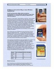
In addition to the <strong>SD</strong> Memory Card, there is the <strong>SD</strong> I/O (<strong>SD</strong>IO) Card. The <strong>SD</strong>IO Card specification is<br />
defined in a separate specification named: "<strong>SD</strong>IO Card <strong>Specification</strong>" that can be obtained from the <strong>SD</strong><br />
Association. The <strong>SD</strong>IO <strong>Specification</strong> defines an <strong>SD</strong> card that may contain interfaces between various<br />
I/O units and an <strong>SD</strong> Host. The <strong>SD</strong>IO card may contain memory storage capability as well as its I/O<br />
functionality. The Memory portion of <strong>SD</strong>IO card shall be fully compatible to the given <strong>Physical</strong> <strong>Layer</strong><br />
<strong>Specification</strong>. The <strong>SD</strong>IO card is based on and compatible with the <strong>SD</strong> Memory card. This compatibility<br />
includes mechanical, electrical, power, signalling, and software. The intent of the <strong>SD</strong> I/O card is to<br />
provide high-speed data I/O with low power consumption for mobile electronic devices. A primary goal is<br />
that an I/O card inserted into a non-<strong>SD</strong>IO aware host will cause no physical damage or disruption of<br />
that device or its software. In this case, the I/O card should simply be ignored. Once inserted into an<br />
<strong>SD</strong>IO aware host, the detection of the card will be via the normal means described in the given <strong>Physical</strong><br />
<strong>Layer</strong> <strong>Specification</strong> with some extensions that are described in the <strong>SD</strong>IO <strong>Specification</strong>.<br />
The <strong>SD</strong> Memory Card communication is based on an advanced 9-pin interface (Clock, Command,<br />
4xData and 3xPower lines) designed to operate in at maximum operating frequency of 50 MHz and low<br />
voltage range. The communication protocol is defined as a part of this specification.<br />
The <strong>SD</strong> <strong><strong>Specification</strong>s</strong> are divided into several documents. The <strong>SD</strong> <strong><strong>Specification</strong>s</strong> documentation<br />
structure is given in Figure 1-1.<br />
Application <strong><strong>Specification</strong>s</strong><br />
<strong>Part</strong> 4 Audio <strong>Part</strong> 8 Video Other Applications<br />
<strong>Part</strong> 3 Security<br />
<strong>Part</strong> 1 <strong>Physical</strong> <strong>Layer</strong><br />
Mechanical Addenda<br />
e<strong>SD</strong> Addendum (Embedded)<br />
<strong>Part</strong> 2 File System<br />
<strong>Part</strong> A1<br />
Advanced<br />
Security <strong>SD</strong><br />
Extension<br />
Figure 1-1: <strong>SD</strong> <strong><strong>Specification</strong>s</strong> Documentation Structure<br />
<strong>Part</strong> E1 <strong>SD</strong>IO<br />
• Audio <strong>Specification</strong>:<br />
This specification, along with other application specifications, describes the specification of a specific<br />
application (in this case - Audio Application) and the requirements to implement it.<br />
• File System <strong>Specification</strong>:<br />
The specification describes the specification of the file format structure of the data saved in the <strong>SD</strong><br />
Memory Card (in User Area and Protected Area).<br />
1
©Copyright 2001-2010 <strong>SD</strong> Group (Panasonic, SanDisk, Toshiba) and <strong>SD</strong> Card Association<br />
<strong>Physical</strong> <strong>Layer</strong> <strong>Simplified</strong> <strong>Specification</strong> Version 3.01<br />
• Security <strong>Specification</strong>:<br />
The specification describes the content protection mechanism and the application-specific commands<br />
that support it.<br />
• <strong>Physical</strong> <strong>Layer</strong> <strong>Specification</strong> (this document):<br />
The specification describes the physical interface and the command protocol used by the <strong>SD</strong> Memory<br />
Card.<br />
The purpose of the <strong>Physical</strong> <strong>Layer</strong> specification is to define the <strong>SD</strong> Memory Card, its environment, and<br />
handling.<br />
The document is divided into several portions. Chapter 3 gives a general overview of the system<br />
concepts. The common <strong>SD</strong> Memory Card characteristics are described in Chapter 0. As this description<br />
defines an overall set of card properties, we recommend using the product documentation in parallel.<br />
The card registers are described in Chapter 5.<br />
Chapter 6 defines the electrical parameters of the <strong>SD</strong> Memory Card's hardware interface.<br />
Mechanical <strong>Specification</strong> described in Chapter 8 in Version 2.00 is moved to the Standard Size<br />
Mechanical Addendum.<br />
There are three mechanical addenda depend on form factors.<br />
(1) Standard Size Mechanical Addendum<br />
(2) mini<strong>SD</strong> Mechanical Addendum<br />
(3) micro<strong>SD</strong> Mechanical Addendum<br />
Un-removable memory device for embedded application is defined by the e<strong>SD</strong> Addendum.<br />
As used in this document, "shall" or "will" denote a mandatory provision of the standard. "Should"<br />
denotes a provision that is recommended but is not mandatory. "May" denotes a feature, which may or<br />
may not be present–at the option of the implementer–and whose presence does not preclude<br />
compliance.<br />
• Mc-EX Interface <strong>Specification</strong>: (This section was added in version 1.10)<br />
<strong>Part</strong> A1 of the <strong>SD</strong> memory card specification (refer to Figure 1-1) serves as an extension to the <strong>SD</strong> card<br />
<strong>Physical</strong> <strong>Layer</strong> <strong>Specification</strong> and provides all of the definitions required to transfer the Mobile<br />
Commerce Extension (Mc-EX) command packets from the Mc-EX host to the Mc-EX enabled <strong>SD</strong><br />
memory card, and vice versa.<br />
• <strong>SD</strong>IO <strong>Specification</strong><br />
<strong>SD</strong>IO card and embedded <strong>SD</strong>IO are specified based on the <strong>Physical</strong> <strong>Layer</strong> <strong>Specification</strong> and<br />
modifications and extensions are described in the <strong>Part</strong> E1 <strong>SD</strong>IO <strong>Specification</strong>.<br />
2
©Copyright 2001-2010 <strong>SD</strong> Group (Panasonic, SanDisk, Toshiba) and <strong>SD</strong> Card Association<br />
<strong>Physical</strong> <strong>Layer</strong> <strong>Simplified</strong> <strong>Specification</strong> Version 3.01<br />
2. System Features<br />
• Targeted for portable and stationary applications<br />
• Capacity of Memory<br />
(1) Standard Capacity <strong>SD</strong> Memory Card (<strong>SD</strong>SC): Up to and including 2 GB<br />
(2) High Capacity <strong>SD</strong> Memory Card (<strong>SD</strong>HC): More than 2GB and up to and including 32GB<br />
(3) Extended Capacity <strong>SD</strong> Memory Card (<strong>SD</strong>XC): More than 32GB and up to and including 2TB<br />
• Voltage range:<br />
High Voltage <strong>SD</strong> Memory Card – Operating voltage range: 2.7-3.6 V<br />
• Designed for read-only and read/write cards.<br />
• Bus Speed Mode (using 4 parallel data lines)<br />
(1) Default Speed mode: 3.3V signaling, Frequency up to 25 MHz, up to 12.5 MB/sec<br />
(2) High Speed mode: 3.3V signaling, Frequency up to 50 MHz, up to 25 MB/sec<br />
(3) <strong>SD</strong>R12: 1.8V signaling, Frequency up to 25 MHz, up to 12.5MB/sec<br />
(4) <strong>SD</strong>R25: 1.8V signaling, Frequency up to 50 MHz, up to 25MB/sec<br />
(5) <strong>SD</strong>R50: 1.8V signaling, Frequency up to 100 MHz, up to 50MB/sec<br />
(6) <strong>SD</strong>R104: 1.8V signaling, Frequency up to 208 MHz, up to 104MB/sec<br />
(7) DDR50: 1.8V signaling, Frequency up to 50 MHz, sampled on both clock edges, up to<br />
50MB/sec<br />
• Switch function command supports Bus Speed Mode, Command System, Drive Strength, and<br />
future functions<br />
• Correction of memory field errors<br />
• Card removal during read operation will never harm the content<br />
• Content Protection Mechanism - Complies with highest security of <strong>SD</strong>MI standard.<br />
• Password Protection of cards (CMD42 - LOCK_UNLOCK)<br />
• Write Protect feature using mechanical switch<br />
• Built-in write protection features (permanent and temporary)<br />
• Card Detection (Insertion/Removal)<br />
• Application specific commands<br />
• Comfortable erase mechanism<br />
3
©Copyright 2001-2010 <strong>SD</strong> Group (Panasonic, SanDisk, Toshiba) and <strong>SD</strong> Card Association<br />
<strong>Physical</strong> <strong>Layer</strong> <strong>Simplified</strong> <strong>Specification</strong> Version 3.01<br />
• Protocol attributes of the communication channel:<br />
<strong>SD</strong> Memory Card Communication Channel<br />
Six-wire communication channel<br />
(clock, command, 4 data lines)<br />
Error-protected data transfer<br />
Single or Multiple block oriented data transfer<br />
• <strong>SD</strong> Memory Card Form-factor<br />
There are three <strong>Part</strong> 1 mechanical addenda as follows:<br />
Standard Size <strong>SD</strong> Memory Card: Specified in "<strong>Part</strong> 1 Standard Size <strong>SD</strong> Card Addendum"<br />
mini<strong>SD</strong> Memory Card: Specified in "<strong>Part</strong> 1 mini<strong>SD</strong> Card Addendum"<br />
micro<strong>SD</strong> Memory Card: Specified in "<strong>Part</strong> 1 micro<strong>SD</strong> Card Addendum"<br />
• Standard Size <strong>SD</strong> Memory Card thickness is defined as both 2.1 mm (normal) and 1.4 mm (Thin<br />
<strong>SD</strong> Memory Card).<br />
4
©Copyright 2001-2010 <strong>SD</strong> Group (Panasonic, SanDisk, Toshiba) and <strong>SD</strong> Card Association<br />
<strong>Physical</strong> <strong>Layer</strong> <strong>Simplified</strong> <strong>Specification</strong> Version 3.01<br />
3. <strong>SD</strong> Memory Card System Concept<br />
Description here is a blank for the <strong>Simplified</strong> <strong>Specification</strong>.<br />
3.1 Read-Write Property<br />
In terms of read-write property, two types of <strong>SD</strong> Memory Cards are defined:<br />
• Read/Write (RW) cards (Flash, One Time Programmable - OTP, Multiple Time Programmable -<br />
MTP). These cards are typically sold as blank (empty) media and are used for mass data storage,<br />
end user video, audio or digital image recording<br />
• Read Only Memory (ROM) cards. These cards are manufactured with fixed data content. They are<br />
typically used as a distribution media for software, audio, video etc.<br />
3.2 Supply Voltage<br />
In terms of operating supply voltage, one type of <strong>SD</strong> Memory Cards is defined:<br />
• High Voltage <strong>SD</strong> Memory Cards that can operate within the voltage range of 2.7-3.6 V.<br />
3.3 Card Capacity<br />
3.3.1 User Area and Protected Area<br />
<strong>SD</strong> Memory Card has two accessible independent areas: User Area and Protected Area. User Area is<br />
main memory area and Protected Area can be accessed by the authentication defined by the <strong>Part</strong> 3<br />
Security <strong>Specification</strong>. Card Capacity means the sum of User Area Capacity and Protected Area<br />
Capacity.<br />
3.3.2 Card Capacity Classification<br />
In terms of card capacity, three types of <strong>SD</strong> Memory Cards are defined:<br />
• Standard Capacity <strong>SD</strong> Memory Card (<strong>SD</strong>SC) supports capacity up to and including 2 G bytes (2 31<br />
bytes). All versions of the <strong>Physical</strong> <strong>Layer</strong> <strong><strong>Specification</strong>s</strong> define the Standard Capacity <strong>SD</strong> Memory<br />
Card.<br />
• High Capacity <strong>SD</strong> Memory Card (<strong>SD</strong>HC) supports capacity more than 2 G bytes (2 31 bytes) up to 32<br />
G bytes and is defined from the <strong>Physical</strong> <strong>Layer</strong> <strong>Specification</strong> Version 2.00.<br />
• Extended Capacity <strong>SD</strong> Memory Card (<strong>SD</strong>XC) supports more than 32 G bytes (2 35 bytes) up to 2TB.<br />
Only hosts that are compliant to the <strong>Physical</strong> <strong>Layer</strong> <strong>Specification</strong> Version 2.00 or later and the File<br />
System <strong>Specification</strong> Ver2.00 or higher can access High Capacity <strong>SD</strong> Memory Cards and Extended<br />
Capacity <strong>SD</strong> Memory Cards. Other hosts fail to initialize High Capacity <strong>SD</strong> Memory Cards and<br />
Extended Capacity <strong>SD</strong> Memory Cards.<br />
Only hosts that are compliant to the <strong>Physical</strong> <strong>Layer</strong> <strong>Specification</strong> Version 3.00 or higher and the File<br />
System <strong>Specification</strong> Ver3.00 or later (exFAT supported) can access Extended Capacity <strong>SD</strong> Memory<br />
Note:<br />
1. The <strong>Part</strong> 1 <strong>Physical</strong> <strong>Layer</strong> <strong>Specification</strong> Version 3.00 and <strong>Part</strong> 2 File System <strong>Specification</strong> Version<br />
3.00 allow Standard Capacity <strong>SD</strong> Memory Cards to have capacity up to and including 2 GB, High<br />
Capacity <strong>SD</strong> Memory Cards to have capacity up to and including 32 GB and Extended Capacity<br />
<strong>SD</strong> Memory Card to have capacity up to 2 TB.<br />
2. Hosts that can access (read and/or write) <strong>SD</strong> Memory Cards with a capacity greater than 2 GB<br />
and up to and including 32 GB, shall also be able to access <strong>SD</strong> Memory Cards with a capacity of<br />
2 GB or less.<br />
3. Hosts that can access (read and/or write) <strong>SD</strong> Memory Cards with a capacity greater than 32 GB<br />
and up to 2 TB, shall also be able to access <strong>SD</strong> Memory Cards with a capacity of 32 GB or less.<br />
5
©Copyright 2001-2010 <strong>SD</strong> Group (Panasonic, SanDisk, Toshiba) and <strong>SD</strong> Card Association<br />
<strong>Physical</strong> <strong>Layer</strong> <strong>Simplified</strong> <strong>Specification</strong> Version 3.01<br />
3.4 Speed Class<br />
Five Speed Classes are defined and indicate minimum performance of the cards<br />
• Class 0 - These class cards do not specify performance. It includes all the legacy cards prior to<br />
this specification, regardless of its performance<br />
• Class 2 is more than or equal to 2 MB/sec performance<br />
• Class 4 is more than or equal to 4 MB/sec performance<br />
• Class 6 is more than or equal to 6 MB/sec performance<br />
• Class 10 is more than or equal to 10 MB/sec performance<br />
High and Extended Capacity <strong>SD</strong> Memory Cards shall support Speed Class <strong>Specification</strong> and have<br />
performance more than or equal to Class 2.<br />
Note that the unit of performance [MB/sec] indicates 1000x1000 [Byte/sec] while the unit of data size<br />
[MB] indicates 1024x1024 [Byte]. This is because the maximum <strong>SD</strong> Bus speed is specified by the<br />
maximum <strong>SD</strong> clock frequency (25 [MB/sec] = 25000000 [Byte/sec] at 50 MHz) and data size is based<br />
on memory boundary (power of 2).<br />
3.5 Bus Topology<br />
Description here is a blank for the <strong>Simplified</strong> <strong>Specification</strong>.<br />
6
©Copyright 2001-2010 <strong>SD</strong> Group (Panasonic, SanDisk, Toshiba) and <strong>SD</strong> Card Association<br />
<strong>Physical</strong> <strong>Layer</strong> <strong>Simplified</strong> <strong>Specification</strong> Version 3.01<br />
3.6 Bus Protocol<br />
3.6.1 <strong>SD</strong> Bus<br />
Communication over the <strong>SD</strong> bus is based on command and data bit streams that are initiated by a start<br />
bit and terminated by a stop bit.<br />
• Command: a command is a token that starts an operation. A command is sent from the host either<br />
to a single card (addressed command) or to all connected cards (broadcast command). A command<br />
is transferred serially on the CMD line.<br />
• Response: a response is a token that is sent from an addressed card, or (synchronously) from all<br />
connected cards, to the host as an answer to a previously received command. A response is<br />
transferred serially on the CMD line.<br />
• Data: data can be transferred from the card to the host or vice versa. Data is transferred via the<br />
data lines.<br />
Figure 3-1: "no response" and "no data" Operations<br />
Card addressing is implemented using a session address, assigned to the card during the initialization<br />
phase. The structure of commands, responses and data blocks is described in Chapter 4. The basic<br />
transaction on the <strong>SD</strong> bus is the command/response transaction (refer to Figure 3-1). This type of bus<br />
transaction transfers their information directly within the command or response structure. In addition,<br />
some operations have a data token.<br />
Data transfers to/from the <strong>SD</strong> Memory Card are done in blocks. Data blocks are always succeeded by<br />
CRC bits. Single and multiple block operations are defined. Note that the Multiple Block operation mode<br />
is better for faster write operation. A multiple block transmission is terminated when a stop command<br />
follows on the CMD line. Data transfer can be configured by the host to use single or multiple data lines.<br />
CMD<br />
from<br />
host<br />
to card<br />
from<br />
card<br />
to host<br />
data from card<br />
to host<br />
stop command<br />
stops data transfer<br />
command response command response<br />
DAT<br />
data block crc data block crc data block crc<br />
block read operation<br />
multiple block read operation<br />
data stop operation<br />
Figure 3-2: (Multiple) Block Read Operation<br />
The block write operation uses a simple busy signaling of the write operation duration on the DAT0 data<br />
line (see Figure 3-3) regardless of the number of data lines used for transferring the data.<br />
7
©Copyright 2001-2010 <strong>SD</strong> Group (Panasonic, SanDisk, Toshiba) and <strong>SD</strong> Card Association<br />
<strong>Physical</strong> <strong>Layer</strong> <strong>Simplified</strong> <strong>Specification</strong> Version 3.01<br />
Figure 3-3: (Multiple) Block Write Operation<br />
Command tokens have the following coding scheme:<br />
Figure 3-4: Command Token Format<br />
Each command token is preceded by a start bit (0) and succeeded by an end bit (1). The total length is<br />
48 bits. Each token is protected by CRC bits so that transmission errors can be detected and the<br />
operation may be repeated.<br />
Response tokens have one of four coding schemes, depending on their content. The token length is<br />
either 48 or 136 bits. The detailed commands and response definition is given in Chapter 4.7. The CRC<br />
protection algorithm for block data is a 16-bit CCITT polynomial. All allowed CRC types are described in<br />
Chapter 4.5.<br />
transmitter bit:<br />
'0'=card response<br />
start bit:<br />
always'0'<br />
Response content: mirrored command and status information<br />
(R1 response), OCR register (R3 response) or<br />
RCA (R6), protected by a 7bit CRC checksum<br />
end bit:<br />
always '1'<br />
R1, R3,R6<br />
0 0 CONTENT 1<br />
total length=48 bits<br />
end bit:<br />
always '1'<br />
R2<br />
0 0 CONTENT=CID or C<strong>SD</strong><br />
CRC<br />
1<br />
total length=136 bits<br />
Figure 3-5: Response Token Format<br />
In the CMD line the Most Significant Bit (MSB) is transmitted first, the Least Significant Bit (LSB) is the<br />
last.<br />
When the wide bus option is used, the data is transferred 4 bits at a time (refer to Figure 3-7). Start and<br />
end bits, as well as the CRC bits, are transmitted for every one of the DAT lines. CRC bits are<br />
calculated and checked for every DAT line individually. The CRC status response and Busy indication<br />
will be sent by the card to the host on DAT0 only (DAT1-DAT3 during that period are don't care).<br />
8
©Copyright 2001-2010 <strong>SD</strong> Group (Panasonic, SanDisk, Toshiba) and <strong>SD</strong> Card Association<br />
<strong>Physical</strong> <strong>Layer</strong> <strong>Simplified</strong> <strong>Specification</strong> Version 3.01<br />
There are two types of Data packet format for the <strong>SD</strong> card.<br />
(1) Usual data (8-bit width): The usual data (8-bit width) are sent in LSB (Least Significant Byte) first,<br />
MSB (Most Significant Byte) last sequence. But in the individual byte, it is MSB (Most Significant<br />
Bit) first, LSB (Least Significant Bit) last.<br />
(2) Wide width data (<strong>SD</strong> Memory Register): The wide width data is shifted from the MSB bit.<br />
Figure 3-6: Data Packet Format - Usual Data<br />
9
©Copyright 2001-2010 <strong>SD</strong> Group (Panasonic, SanDisk, Toshiba) and <strong>SD</strong> Card Association<br />
<strong>Physical</strong> <strong>Layer</strong> <strong>Simplified</strong> <strong>Specification</strong> Version 3.01<br />
2. Data Packet Format for Wide Width Data (Ex. ACMD13)<br />
b511<br />
Ex. <strong>SD</strong> Status<br />
Wide Width<br />
Data<br />
Ex.<br />
[<strong>SD</strong> memory]<br />
ACMD13(<strong>SD</strong> Status),<br />
ACMD51(SCR),<br />
etc<br />
b0<br />
Start bit<br />
End bit<br />
DAT0 0 b511 b510 b509 b508<br />
b1 b0 CRC 1<br />
Data Packet Format for Standard Bus (only DAT0 used)<br />
Start bit<br />
End bit<br />
DAT3<br />
0<br />
b511 b507 b503 b499<br />
b7 b3 CRC 1<br />
DAT2<br />
0<br />
b510 b506 b502 b498<br />
b6 b2 CRC 1<br />
DAT1<br />
0<br />
b509 b505 b501 b497<br />
b5 b1 CRC 1<br />
DAT0<br />
0<br />
b508 b504 b500 b496<br />
b4 b0 CRC 1<br />
Data Packet Format for Wide Bus (all four lines used)<br />
Figure 3-7: Data Packet Format - Wide Width Data<br />
3.6.2 SPI Bus<br />
Details of the SPI Bus protocol are described in Chapter 7.<br />
10
©Copyright 2001-2010 <strong>SD</strong> Group (Panasonic, SanDisk, Toshiba) and <strong>SD</strong> Card Association<br />
<strong>Physical</strong> <strong>Layer</strong> <strong>Simplified</strong> <strong>Specification</strong> Version 3.01<br />
3.7 <strong>SD</strong> Memory Card–Pins and Registers<br />
A part of this section is not described.<br />
Each card has a set of information registers (see also Chapter 5 in the <strong>Physical</strong> <strong>Layer</strong> <strong>Specification</strong>):<br />
Name Width Description<br />
CID 128 Card identification number; card individual number for identification (See 5.2).<br />
Mandatory.<br />
RCA 1 16 Relative card address; local system address of a card, dynamically suggested by<br />
the card and approved by the host during initialization (See 5.4). Mandatory.<br />
DSR 16 Driver Stage Register; to configure the card's output drivers (See 5.5). Optional.<br />
C<strong>SD</strong> 128 Card Specific Data; information about the card operation conditions (See 5.3).<br />
Mandatory<br />
SCR 64 <strong>SD</strong> Configuration Register; information about the <strong>SD</strong> Memory Card's Special Features<br />
capabilities (See 5.6). Mandatory<br />
OCR 32 Operation conditions register (See 5.1). Mandatory.<br />
SSR 512 <strong>SD</strong> Status; information about the card proprietary features (See 4.10.2).<br />
Mandatory<br />
CSR 32 Card Status; information about the card status (See 4.10.1). Mandatory<br />
(1) RCA register is not used (available) in SPI mode<br />
Table 3-1: <strong>SD</strong> Memory Card Registers<br />
3.8 ROM Card<br />
ROM Card is defined as read only memory which meets following requirements. A permanent or<br />
temporary write protected writable <strong>SD</strong> memory card does not belong to this category.<br />
3.8.1 Register Setting Requirements<br />
Table 3-3 shows register setting requirements for ROM Card.<br />
Register Field Value Comment<br />
<strong>SD</strong> Status <strong>SD</strong>_CARD_TYPE 0001h <strong>SD</strong> ROM Card<br />
CCC bit 4 0 Class4 block write<br />
C<strong>SD</strong> CCC bit 5 0 Class5 erase<br />
CCC bit 6 0 Class6 write protection<br />
CCC bit 7 0 or 1 Class7 lock card<br />
PERM_WRITE_PROT 1 Permanent Write Protect<br />
SCR <strong>SD</strong>_SECURITY 0 or 2 or 3 Security is optional.<br />
Table 3-2 : Register Setting Requirements for ROM Card<br />
3.8.2 Unsupported Commands<br />
The ROM Card shall treat following commands as unsupported and illegal command.<br />
CMD24, CMD25, CMD27, CMD28, CMD29, CMD30, CMD32, CMD33, CMD38<br />
3.8.3 Optional Commands<br />
The ROM Card can support following commands as optional command.<br />
CMD42, security commands<br />
11
©Copyright 2001-2010 <strong>SD</strong> Group (Panasonic, SanDisk, Toshiba) and <strong>SD</strong> Card Association<br />
<strong>Physical</strong> <strong>Layer</strong> <strong>Simplified</strong> <strong>Specification</strong> Version 3.01<br />
• If CMD42 is not supported, bit 7 of CCC shall be set to 0. CMD42 is treated as illegal command.<br />
• When ROM card supports CMD42, "Unlocking the card" and "Locking the card" functions shall be<br />
supported by presetting the password. LOCK_UNLOCK_FAILED is indicated when receiving the<br />
other unsupported functions of CMD42.<br />
• If security is not supported, <strong>SD</strong>_SECURITY shall be set to 0. The security commands are treated<br />
as illegal command.<br />
• ROM card does not support write and erase to the protected area. Refer to the <strong>Part</strong> 3 Security<br />
<strong>Specification</strong> about security command support of ROM card.<br />
3.8.4 WP Switch<br />
A full-size ROM card does not have WP Switch. Refer to Figure 3-8 in the <strong>Part</strong> 1 Standard Size <strong>SD</strong><br />
Card Mechanical Addendum Ver1.00.<br />
12
©Copyright 2001-2010 <strong>SD</strong> Group (Panasonic, SanDisk, Toshiba) and <strong>SD</strong> Card Association<br />
<strong>Physical</strong> <strong>Layer</strong> <strong>Simplified</strong> <strong>Specification</strong> Version 3.01<br />
3.9 Ultra High Speed Phase I (UHS-I) Card<br />
UHS-I provides up to 104MB/sec performance on 4-bit <strong>SD</strong> bus with the single end driver interface. Card<br />
form factor is the same and existing connector can be used.<br />
3.9.1 UHS-I Operation Modes<br />
• DS - Default Speed up to 25MHz 3.3V signaling<br />
• HS - High Speed up to 50MHz 3.3V signaling<br />
• <strong>SD</strong>R12 - <strong>SD</strong>R up to 25MHz 1.8V signaling<br />
• <strong>SD</strong>R25 - <strong>SD</strong>R up to 50MHz 1.8V signaling<br />
• <strong>SD</strong>R50 - <strong>SD</strong>R up to 100MHz 1.8V signaling<br />
• <strong>SD</strong>R104 - <strong>SD</strong>R up to 208MHz 1.8V signaling<br />
• DDR50 - DDR up to 50MHz 1.8V signaling<br />
Note : Timing in 1.8V signaling is different from that of 3.3V signaling.<br />
3.9.2 UHS-I Card Types<br />
UHS-I supports two card Types:<br />
• UHS50<br />
• UHS104<br />
UHS-I is not applied to <strong>SD</strong>SC card but can be applied to <strong>SD</strong>HC and <strong>SD</strong>XC card.<br />
Figure 3-8 and Figure 3-9 show UHS-I supported modes.<br />
DDR50 is mandatory for micro<strong>SD</strong> form factor and optional for Standard size <strong>SD</strong> form factor<br />
UHS50 Card<br />
DS<br />
HS<br />
<strong>SD</strong>R12<br />
<strong>SD</strong>R25<br />
DDR50<br />
DS: Default Speed Mode<br />
HS: High Speed Mode<br />
Signal Voltage<br />
<strong>SD</strong>R50 3.3V 1.8V<br />
UHS104 Card<br />
DS<br />
HS<br />
<strong>SD</strong>R12<br />
<strong>SD</strong>R25<br />
DDR50<br />
<strong>SD</strong>R50<br />
<strong>SD</strong>R104<br />
25MHz 50MHz 100MHz 208MHz<br />
Frequency<br />
Figure 3-8 : UHS-I Card Type Modes of Operation versus Frequency Range<br />
13
©Copyright 2001-2010 <strong>SD</strong> Group (Panasonic, SanDisk, Toshiba) and <strong>SD</strong> Card Association<br />
<strong>Physical</strong> <strong>Layer</strong> <strong>Simplified</strong> <strong>Specification</strong> Version 3.01<br />
UHS50 Card<br />
DS<br />
HS<br />
<strong>SD</strong>R12<br />
<strong>SD</strong>R25<br />
DS: Default Speed Mode<br />
HS: High Speed Mode<br />
Signal Voltage<br />
<strong>SD</strong>R50 3.3V 1.8V<br />
DDR50<br />
UHS104 Card<br />
DS<br />
HS<br />
<strong>SD</strong>R12<br />
<strong>SD</strong>R25<br />
<strong>SD</strong>R50<br />
DDR50<br />
<strong>SD</strong>R104<br />
12MB/s 25MB/s 50MB/s 104MB/s<br />
Throughput<br />
Figure 3-9 : UHS-I Card Type Modes of Operation versus Throughput<br />
3.9.3 Host and Card Combination<br />
Host may use <strong>SD</strong>R50, DDR50 and <strong>SD</strong>R104 modes with either UHS50 Card or UHS104 Card.<br />
Table 3-3 shows usable UHS performance depends on the combination of host and card. UHS-I for<br />
removable card is presumed that one card is connected to a <strong>SD</strong> bus. Maximum performance of up to<br />
104MB/s is possible only if host supports <strong>SD</strong>R104 mode and card is UHS104 Card (supports <strong>SD</strong>R104<br />
mode). If card is a UHS50 Card or if host doesn't support <strong>SD</strong>R104 mode, performance is limited to<br />
50MB/s (<strong>SD</strong>R104 mode cannot be used).<br />
Host may use DDR50 mode with UHS50 Card and UHS104 Card in micro<strong>SD</strong> form factors.<br />
Host types:<br />
<strong>SD</strong>R-FD – <strong>SD</strong>R signaling, fixed-delay (can't use tuning)<br />
<strong>SD</strong>R-VD – <strong>SD</strong>R signaling, variable-delay (can use tuning)<br />
DDR – DDR signaling<br />
Host type<br />
Card type<br />
UHS50 card<br />
micro<strong>SD</strong><br />
UHS104 card<br />
micro<strong>SD</strong><br />
UHS50 card<br />
Full-size <strong>SD</strong><br />
UHS104 card<br />
Full-size <strong>SD</strong><br />
HOST-<strong>SD</strong>R-FD<br />
(<strong>SD</strong>R, fixed-delay)<br />
HOST-<strong>SD</strong>R-VD<br />
(<strong>SD</strong>R, variable-delay)<br />
HOST-DDR<br />
(DDR)<br />
<strong>SD</strong>R50 ≤ 100MHz <strong>SD</strong>R50 ≤ 100MHz + tuning DDR50 ≤ 50MHz<br />
<strong>SD</strong>R50 ≤ 100MHz <strong>SD</strong>R104 ≤ 208MHz + tuning DDR50 ≤ 50MHz<br />
<strong>SD</strong>R50 ≤ 100MHz <strong>SD</strong>R50 ≤ 100MHz + tuning Optional<br />
<strong>SD</strong>R50 ≤ 100MHz <strong>SD</strong>R104 ≤ 208MHz + tuning Optional<br />
Table 3-3 : Host and Card Combinations<br />
14
©Copyright 2001-2010 <strong>SD</strong> Group (Panasonic, SanDisk, Toshiba) and <strong>SD</strong> Card Association<br />
<strong>Physical</strong> <strong>Layer</strong> <strong>Simplified</strong> <strong>Specification</strong> Version 3.01<br />
3.9.4 Bus Speed Modes Selection Sequence<br />
Power on<br />
CMD0<br />
CMD8<br />
ACMD41<br />
CMD11<br />
Once signal voltage is switched to 1.8V, the card continues 1.8V signaling<br />
regardless of CMD0. Power cycle resets the signal voltage to 3.3V.<br />
After Switching 1.8V singling, the card cannot be changed to SPI mode.<br />
Host requests card to change 1.8V signal voltage by ACMD41.<br />
A status is indicated in the response whether voltage switch is accepted.<br />
If voltage switch is accepted by ACMD41, CMD11 invokes voltage<br />
switching sequence. If it is completed, the card enters <strong>SD</strong>R12 (default).<br />
CMD2<br />
CMD3<br />
CMD7<br />
CMD42<br />
ACMD6<br />
CMD6<br />
CMD19<br />
If the CARD_IS_LOCKED status is set to 1 in the response of CMD7,<br />
CMD42 is required before ACMD6 to unlock the card.<br />
UHS-I supports only 4-bit mode. Host shall select 4-bit mode by ACMD6.<br />
Driver Strength is selected by CMD6 Function Group 3.<br />
Bus Speed Mode is selected by CMD6 Function Group 1.<br />
Current Limit is selected by CMD6 Function Group 4.<br />
CMD19 sends a tuning block to the host to determine sampling point.<br />
UHS50 and UHS104 cards support CMD19 in 1.8V signaling. Sampling<br />
clock tuning is required for UHS104 host and optional for UHS50 host.<br />
Figure 3-10 : Command Sequence to Use UHS-I<br />
Figure 3-10 shows command sequence to use a UHS-I. After power cycle, card is in 3.3V signaling<br />
mode. The first CMD0 selects the bus mode; <strong>SD</strong> mode or SPI mode. 1.8V signaling mode can be<br />
entered only in <strong>SD</strong> mode. Once the card enters 1.8V signaling mode, the card cannot be switched to<br />
SPI mode or 3.3V signaling without power cycle. If the card receives CMD0, card returns to Idle state<br />
but still work with <strong>SD</strong>R12 timing. UHS-I is provided in <strong>SD</strong> mode but not in SPI mode.<br />
As higher bus speed requires low level signaling, UHS-I adopts 1.8V signaling level for <strong>SD</strong>R50, DDR50<br />
and <strong>SD</strong>R104 modes. Still card is supplied with 3.3V by the host and 1.8V signaling level for <strong>SD</strong>CLK,<br />
CMD and DAT[3:0] lines is converted from 3.3V power line. To avoid voltage mismatch between host<br />
and card, signaling level is changed by voltage switch sequence at the initialization. The host and card<br />
communicate using ACMD41 whether host and card support 1.8V signaling mode. Support of 1.8V<br />
signaling both host and card means UHS-I can be used. CMD11 invokes the voltage switch sequence.<br />
The card enters UHS-I mode and card input and output timings are changed (<strong>SD</strong>R12 in default) when<br />
the voltage switch sequence is completed successfully. (Refer to Section 4.2.4 for more detail.)<br />
Only 4-bit bus mode is supported in UHS-I except CMD42. If the card is locked, host needs to unlock<br />
the card by CMD42 in 1-bit mode and then needs to issue ACMD6 to change 4-bit bus mode. Operating<br />
in 1-bit mode is not assured.<br />
Host can choose suitable output driver strength by CMD6 Function Group 3.<br />
Host can choose one of UHS-I modes by CMD6 Function Group 1. Each UHS-I mode is specified by<br />
the maximum frequency, sampling edges (rising-only or both) and maximum current consumption for<br />
compatibility with existing cards. Host can choose one of UHS-I mode depending on capability of<br />
generating <strong>SD</strong>CLK frequency and capacity of power supply host supported.<br />
CMD19 can be executed in transfer state of 1.8V signaling mode while the card is unlocked. The other<br />
case, CMD19 is treated as illegal command.<br />
15
©Copyright 2001-2010 <strong>SD</strong> Group (Panasonic, SanDisk, Toshiba) and <strong>SD</strong> Card Association<br />
<strong>Physical</strong> <strong>Layer</strong> <strong>Simplified</strong> <strong>Specification</strong> Version 3.01<br />
3.9.5 UHS System Block Diagram<br />
This section is a blank for the <strong>Simplified</strong> <strong>Specification</strong>.<br />
16
©Copyright 2001-2010 <strong>SD</strong> Group (Panasonic, SanDisk, Toshiba) and <strong>SD</strong> Card Association<br />
<strong>Physical</strong> <strong>Layer</strong> <strong>Simplified</strong> <strong>Specification</strong> Version 3.01<br />
3.9.6 Summary of Bus Speed Mode<br />
Table 3-4 shows the card requirements regarding Bus Speed modes selected by CMD6 function group<br />
1. The maximum frequency and the maximum current are determined by CMD6.<br />
Bus Speed<br />
Mode *1<br />
Max. Bus<br />
Speed<br />
Max. Clock<br />
Frequency<br />
Signal<br />
Voltage<br />
Max. Current *2<br />
[mA/3.6V VDD]<br />
[MB/s] [MHz] [V] <strong>SD</strong>SC *3 <strong>SD</strong>HC *4 <strong>SD</strong>XC *5<br />
<strong>SD</strong>R104 104 208 1.8 - 800 *6 800 *6<br />
<strong>SD</strong>R50 50 100 1.8 - 400 400<br />
DDR50 50 50 1.8 - 400 400<br />
<strong>SD</strong>R25 25 50 1.8 - 200 200<br />
<strong>SD</strong>R12 12.5 25 1.8 - 100 100/150 *7<br />
High Speed 25 50 3.3 200 200 200<br />
Default Speed 12.5 25 3.3 100 100 100/150 *7<br />
*1: The card supports a UHS-I mode shall support all lower UHS-I modes.<br />
*2: Host can control current by the current limit function in CMD6 (Refer to Section 4.3.10.3).<br />
*3: <strong>SD</strong>SC stands for <strong>SD</strong> Standard Capacity Memory Card and<br />
*4: <strong>SD</strong>HC stands for <strong>SD</strong> High Capacity Memory Card.<br />
*5: <strong>SD</strong>XC stands for <strong>SD</strong> Extended Capacity Memory Card.<br />
*6: Detail of socket handling 800mA will be specifying in mechanical addenda.<br />
*7: Host can select either max. current by XPC in ACMD41 (Refer to Section 4.2.3.1).<br />
In SPI mode, XPC is not supported and the current shall be up to 100mA.<br />
Table 3-4 : Bus Speed Modes<br />
DS - Default Speed up to 25MHz 3.3V signaling<br />
HS - High Speed up to 50MHz 3.3V signaling<br />
<strong>SD</strong>R12 - <strong>SD</strong>R up to 25MHz 1.8V signaling<br />
<strong>SD</strong>R25 - <strong>SD</strong>R up to 50MHz 1.8V signaling<br />
<strong>SD</strong>R50 - <strong>SD</strong>R up to 100MHz 1.8V signaling<br />
<strong>SD</strong>R104 - <strong>SD</strong>R up to 208MHz 1.8V signaling<br />
DDR50 - DDR up to 50MHz 1.8V signaling<br />
Detail temperature specification is described in the mechanical addenda.<br />
Table 3-5 clarifies option / mandatory of bus speed mode for each card capacity type.<br />
Card Classification DS HS <strong>SD</strong>R50 <strong>SD</strong>R104 DDR50<br />
<strong>SD</strong>SC M O N/A N/A N/A<br />
Non UHS-I M O N/A N/A N/A<br />
UHS50 M M M N/A O (Standard <strong>SD</strong>)<br />
<strong>SD</strong>HC<br />
M (micro<strong>SD</strong>)<br />
UHS104 M M M M O (Standard <strong>SD</strong>)<br />
M (micro<strong>SD</strong>)<br />
Non UHS-I M O N/A N/A N/A<br />
UHS50 M M M N/A O (Standard <strong>SD</strong>)<br />
<strong>SD</strong>XC<br />
M (micro<strong>SD</strong>)<br />
UHS104 M M M M O (Standard <strong>SD</strong>)<br />
M (micro<strong>SD</strong>)<br />
M: Mandatory, O: Optional, N/A: Not Available<br />
Table 3-5 : Bus Speed Mode Option / Mandatory<br />
17
©Copyright 2001-2010 <strong>SD</strong> Group (Panasonic, SanDisk, Toshiba) and <strong>SD</strong> Card Association<br />
<strong>Physical</strong> <strong>Layer</strong> <strong>Simplified</strong> <strong>Specification</strong> Version 3.01<br />
4. <strong>SD</strong> Memory Card Functional Description<br />
4.1 General<br />
All communication between host and cards is controlled by the host (master). The host sends commands<br />
of two types: broadcast and addressed (point-to-point) commands.<br />
• Broadcast commands<br />
Broadcast commands are intended for all cards. Some of these commands require a response.<br />
• Addressed (point-to-point) commands<br />
The addressed commands are sent to the addressed card and cause a response from this card.<br />
A general overview of the command flow is shown in Figure 4-1 for card identification mode and in<br />
Figure 4-9 for data transfer mode. The commands are listed in the command tables (Table 4-19-<br />
Table 4-28). The dependencies between current state, received command, and following state are<br />
listed in Table 4-29. In the following sections, the various card operation modes will be described<br />
first. Afterwards, the restrictions for controlling the clock signal are defined. All <strong>SD</strong> Memory Card<br />
commands, along with the corresponding responses, state transitions, error conditions and timings<br />
are presented in the succeeding sections.<br />
Two operation modes are defined for the <strong>SD</strong> Memory Card system (host and cards):<br />
• Card identification mode<br />
The host will be in card identification mode after reset and while it is looking for new cards on the<br />
bus. Cards will be in this mode after reset until the SEND_RCA command (CMD3) is received.<br />
• Data transfer mode<br />
Cards will enter data transfer mode after their RCA is first published. The host will enter data<br />
transfer mode after identifying all the cards on the bus.<br />
The following table shows the dependencies between operation modes and card states. Each state in<br />
the <strong>SD</strong> Memory Card state diagram (see Figure 4-1) is associated with one operation mode:<br />
Card state<br />
Operation mode<br />
Inactive State<br />
inactive<br />
Idle State<br />
Ready State<br />
card identification mode<br />
Identification State<br />
Stand-by State<br />
Transfer State<br />
Sending-data State<br />
data transfer mode<br />
Receive-data State<br />
Programming State<br />
Disconnect State<br />
Table 4-1: Overview of Card States vs. Operation Modes<br />
18
©Copyright 2001-2010 <strong>SD</strong> Group (Panasonic, SanDisk, Toshiba) and <strong>SD</strong> Card Association<br />
<strong>Physical</strong> <strong>Layer</strong> <strong>Simplified</strong> <strong>Specification</strong> Version 3.01<br />
4.2 Card Identification Mode<br />
While in card identification mode the host resets all the cards that are in card identification mode,<br />
validates operation voltage range, identifies cards and asks them to publish Relative Card Address<br />
(RCA). This operation is done to each card separately on its own CMD line. All data communication in<br />
the Card Identification Mode uses the command line (CMD) only.<br />
During the card identification process, the card shall operate in the <strong>SD</strong> clock frequency of the<br />
identification clock rate f OD .<br />
4.2.1 Card Reset<br />
The command GO_IDLE_STATE (CMD0) is the software reset command and sets each card into Idle<br />
State regardless of the current card state. Cards in Inactive State are not affected by this command.<br />
After power-on by the host, all cards are in Idle State, including the cards that have been in Inactive<br />
State before.<br />
After power-on or CMD0, all cards' CMD lines are in input mode, waiting for start bit of the next command.<br />
The cards are initialized with a default relative card address (RCA=0x0000) and with a default<br />
driver strength with 400KHz clock frequency. In case of 3.3V signaling, default driver strength is<br />
specified by the Driver Stage Register (DSR) if supported and selected highest driving current<br />
capability. In case of 1.8V signaling, default driver strength is specified by type B driver.<br />
4.2.2 Operating Condition Validation<br />
At the start of communication between the host and the card, the host may not know the card supported<br />
voltage and the card may not know whether it supports the current supplied voltage. The host issues a<br />
reset command (CMD0) with a specified voltage while assuming it may be supported by the card. To<br />
verify the voltage, a following new command (CMD8) is defined in the <strong>Physical</strong> <strong>Layer</strong> <strong>Specification</strong><br />
Version 2.00.<br />
SEND_IF_COND (CMD8) is used to verify <strong>SD</strong> Memory Card interface operating condition. The card<br />
checks the validity of operating condition by analyzing the argument of CMD8 and the host checks the<br />
validity by analyzing the response of CMD8 (See Chapter 4.3.13). The supplied voltage is indicated by<br />
VHS filed in the argument. The card assumes the voltage specified in VHS as the current supplied<br />
voltage. Only 1-bit of VHS shall be set to 1 at any given time. Both CRC and check pattern are used for<br />
the host to check validity of communication between the host and the card.<br />
If the card can operate on the supplied voltage, the response echoes back the supply voltage and the<br />
check pattern that were set in the command argument.<br />
If the card cannot operate on the supplied voltage, it returns no response and stays in idle state. It is<br />
mandatory to issue CMD8 prior to first ACMD41 to initialize <strong>SD</strong>HC or <strong>SD</strong>XC Card (See Figure 4-1).<br />
Receipt of CMD8 makes the cards realize that the host supports the <strong>Physical</strong> <strong>Layer</strong> Version 2.00 or<br />
later and the card can enable new functions.<br />
<strong>SD</strong>_SEND_OP_COND (ACMD41) is designed to provide <strong>SD</strong> Memory Card hosts with a mechanism to<br />
identify and reject cards which do not match the V DD range desired by the host. This is accomplished by<br />
the host sending the required V DD voltage window as the operand of this command (See Chapter 5.1).<br />
Cards which cannot perform data transfer in the specified range shall discard themselves from further<br />
bus operations and go into Inactive State. The levels in the OCR register shall be defined accordingly<br />
(See Chapter 5.1). Note that ACMD41 is application specific command; therefore APP_CMD (CMD55)<br />
shall always precede ACMD41. The RCA to be used for CMD55 in idle_state shall be the card's default<br />
RCA = 0x0000.<br />
After the host issues a reset command (CMD0) to reset the card, the host shall issue CMD8 prior to<br />
ACMD41 to re-initialize the <strong>SD</strong> Memory card.<br />
19
©Copyright 2001-2010 <strong>SD</strong> Group (Panasonic, SanDisk, Toshiba) and <strong>SD</strong> Card Association<br />
<strong>Physical</strong> <strong>Layer</strong> <strong>Simplified</strong> <strong>Specification</strong> Version 3.01<br />
Power on<br />
SPI Operation<br />
Mode<br />
CMD0 +<br />
CS Asserted<br />
("0")<br />
Idle State<br />
(idle)<br />
CMD0<br />
from all states except (ina)<br />
If card cannot operate under supplied voltage,<br />
card doesn't respond and return to 'Idle State'<br />
CMD8<br />
It is mandatory for the host compliant<br />
to <strong>Physical</strong> Spec Version 2.00<br />
to send CMD8 before ACMD41<br />
card returns busy (*1) or<br />
host omitted voltage range<br />
No Response<br />
(Non valid command)<br />
Must be a<br />
MultiMediaCard<br />
ACMD41<br />
Ready State<br />
(ready)<br />
CMD11<br />
Inactive<br />
State(ina)<br />
cards with non compatible<br />
voltage range<br />
Start MultiMediaCard<br />
initialization process<br />
starting at CMD1<br />
CMD2<br />
Identification<br />
State(ident)<br />
card executes Voltage<br />
Switch Sequence.<br />
Whether it can be executed<br />
is determined in ACMD41.<br />
card-identification-mode<br />
Card responds with<br />
new RCA<br />
CMD3<br />
data-transfer-mode<br />
Stand-by State<br />
(stby)<br />
CMD3<br />
CMD15<br />
Card responds with<br />
new RCA<br />
from all states in<br />
data-transfer-mode<br />
(*1) Note : Card returns busy when<br />
- Card executes internal initialization process<br />
- Card is High or Extended capacity <strong>SD</strong> Memory Card and host doesn't support<br />
High or Extended capacity<br />
This means that CMD8 is mandatory to initialize High capacity <strong>SD</strong> Memory Card.<br />
Figure 4-1: <strong>SD</strong> Memory Card State Diagram (card identification mode)<br />
By setting the OCR to zero in the argument of ACMD41, the host can query each card and determine<br />
the common voltage range before sending out-of-range cards into the Inactive State (query mode). This<br />
query should be used if the host is able to select a common voltage range or if a notification to the<br />
application of non usable cards in the stack is desired. The card does not start initialization and ignores<br />
HCS in the argument (refer to Section 4.2.3) if ACMD41 is issued as a query. Afterwards, the host may<br />
choose a voltage for operation and reissue ACMD41 with this condition, sending incompatible cards into<br />
the Inactive State.<br />
During the initialization procedure, the host is not allowed to change the operating voltage range. Refer<br />
to the power up sequence as described in Chapter 6.4.<br />
20
©Copyright 2001-2010 <strong>SD</strong> Group (Panasonic, SanDisk, Toshiba) and <strong>SD</strong> Card Association<br />
<strong>Physical</strong> <strong>Layer</strong> <strong>Simplified</strong> <strong>Specification</strong> Version 3.01<br />
4.2.3 Card Initialization and Identification Process<br />
After the bus is activated the host starts card initialization and identification process (See Figure 4-2).<br />
The initialization process starts with <strong>SD</strong>_SEND_OP_COND (ACMD41) by setting its operational<br />
conditions and the HCS bit in the OCR. The HCS (Host Capacity Support) bit set to 1 indicates that the<br />
host supports <strong>SD</strong>HC or <strong>SD</strong>XC Card. The HCS (Host Capacity Support) bit set to 0 indicates that the<br />
host supports neither <strong>SD</strong>HC nor <strong>SD</strong>XC Card.<br />
Receiving of CMD8 expands the ACMD41 function; HCS in the argument and CCS (Card Capacity<br />
Status) in the response. HCS is ignored by cards, which didn't respond to CMD8. However the host<br />
should set HCS to 0 if the card returns no response to CMD8. Standard Capacity <strong>SD</strong> Memory Card<br />
ignores HCS. If HCS is set to 0, <strong>SD</strong>HC and <strong>SD</strong>XC Cards never return ready status (keep busy bit to 0).<br />
The busy bit in the OCR is used by the card to inform the host whether initialization of ACMD41 is<br />
completed. Setting the busy bit to 0 indicates that the card is still initializing. Setting the busy bit to 1<br />
indicates completion of initialization. Card initialization shall be completed within 1 second from the first<br />
ACMD41. The host repeatedly issues ACMD41 for at least 1 second or until the busy bit are set to 1.<br />
The card checks the operational conditions and the HCS bit in the OCR only at the first ACMD41 with<br />
setting voltage window in the argument. While repeating ACMD41, the host shall not issue another<br />
command except CMD0.<br />
If the card responds to CMD8, the response of ACMD41 includes the CCS field information. CCS is<br />
valid when the card returns ready (the busy bit is set to 1). CCS=0 means that the card is <strong>SD</strong>SC.<br />
CCS=1 means that the card is <strong>SD</strong>HC or <strong>SD</strong>XC.<br />
The host performs the same initialization sequence to all of the new cards in the system. Incompatible<br />
cards are sent into Inactive State. The host then issues the command ALL_SEND_CID (CMD2), to each<br />
card to get its unique card identification (CID) number. Card that is unidentified (i.e. which is in Ready<br />
State) sends its CID number as the response (on the CMD line). After the CID was sent by the card it<br />
goes into Identification State. Thereafter, the host issues CMD3 (SEND_RELATIVE_ADDR) asks the<br />
card to publish a new relative card address (RCA), which is shorter than CID and which is used to<br />
address the card in the future data transfer mode. Once the RCA is received the card state changes to<br />
the Stand-by State. At this point, if the host wants to assign another RCA number, it can ask the card to<br />
publish a new number by sending another CMD3 command to the card. The last published RCA is the<br />
actual RCA number of the card.<br />
The host repeats the identification process, i.e. the cycles with CMD2 and CMD3 for each card in the<br />
system.<br />
Initialization of <strong>SD</strong>XC is identical to <strong>SD</strong>HC. User area capacity of <strong>SD</strong>XC card is specified by C_SIZE<br />
and it shall be more than or equal to 32GB.<br />
Application Notes:<br />
The host shall set ACMD41 timeout more than 1 second to abort repeat of issuing ACMD41 when<br />
the card does not indicate ready. The timeout count starts from the first ACMD41 which is set<br />
voltage window in the argument.<br />
21
©Copyright 2001-2010 <strong>SD</strong> Group (Panasonic, SanDisk, Toshiba) and <strong>SD</strong> Card Association<br />
<strong>Physical</strong> <strong>Layer</strong> <strong>Simplified</strong> <strong>Specification</strong> Version 3.01<br />
Power-on<br />
CMD0<br />
No response<br />
CMD8<br />
Card returns response<br />
Ver2.00 or later <strong>SD</strong> Memory Card(voltage mismatch)<br />
or Ver1.X <strong>SD</strong> Memory Card<br />
or not <strong>SD</strong> Memory Card<br />
Ver2.00 or later<br />
<strong>SD</strong> Memory Card<br />
Non-compatible voltage range<br />
or check pattern is not correct<br />
No response<br />
Not <strong>SD</strong> Memory Card<br />
ACMD41<br />
with HCS=0<br />
Unusable<br />
Card is<br />
Card<br />
ready<br />
cards with non compatible<br />
voltage range (card goes to<br />
'ina' state) or time-out<br />
(no response or busy) occurs<br />
Card returns<br />
ready<br />
Ver1.X<br />
Standard Capacity<br />
<strong>SD</strong> Memory Card<br />
Card returns<br />
busy<br />
Card returns<br />
busy<br />
Valid<br />
Response<br />
Card with compatible<br />
Voltage range<br />
ACMD41<br />
with HCS=0or1<br />
Card is<br />
ready<br />
Card returns ready<br />
CCS in<br />
Response<br />
CCS=0<br />
Ver2.00 or later<br />
Standard Capacity<br />
<strong>SD</strong> Memory Card<br />
CCS=1<br />
Unusable<br />
Card<br />
Compatible voltage range<br />
and check pattern is correct<br />
If host supports high capacity, HCS is set to 1<br />
cards with non compatible voltage range<br />
or time-out (no response or busy) occurs<br />
Unusable<br />
Card<br />
Ver2.00 or later<br />
High Capacity or<br />
Extended Capacity<br />
<strong>SD</strong> Memory Card<br />
S18R and S18A <br />
S18R and S18A are negotiated in ACMD41.<br />
S18A is valid only when card returns ready.<br />
S18R=1&S18A=1<br />
CMD11<br />
S18R=0 or S18A=0<br />
CMD2<br />
CMD3<br />
Figure 4-2: Card Initialization and Identification Flow (<strong>SD</strong> mode)<br />
22
©Copyright 2001-2010 <strong>SD</strong> Group (Panasonic, SanDisk, Toshiba) and <strong>SD</strong> Card Association<br />
<strong>Physical</strong> <strong>Layer</strong> <strong>Simplified</strong> <strong>Specification</strong> Version 3.01<br />
4.2.3.1 Initialization Command (ACMD41)<br />
Followings are general rules of the argument of ACMD41:<br />
(1) If the voltage window field (bit 23-0) in the argument is set to zero, it is called "inquiry CMD41" that<br />
does not start initialization and is use for getting OCR. The inquiry ACMD41 shall ignore the other<br />
field (bit 31-24) in the argument.<br />
(2) If the voltage window field (bit 23-0) in the argument is set to non-zero at the first time, it is called<br />
"first ACMD41" that starts initialization. The other field (bit 31-24) in the argument is effective.<br />
(3) The argument of following ACMD41 shall be the same as that of the first ACMD41.<br />
Figure 4-3 shows argument format and Figure 4-4 shows response format. Two new fields are added to<br />
the argument of ACMD41.<br />
If a <strong>SD</strong>XC Card is initialized with XPC=0, the card is operating less than 100mA in Default Speed or<br />
<strong>SD</strong>R12, and if the card does not support Speed Class, Class 0 is indicated in <strong>SD</strong> Status. If a <strong>SD</strong>XC<br />
Card is initialized with XPC=1, the card is operating less than 150mA in Default Speed or <strong>SD</strong>R12, and<br />
the card supports Speed Class. Re-initialization is required to change XPC selection.<br />
UHS-I supported host sets S18R=1 in the argument of ACMD41 to request the card to switch 1.8V<br />
signaling level. UHS-I supports card respond with S18A=1 in the response of ACMD41 and then host<br />
can issue voltage switch command.<br />
(1) Argument of ACMD41<br />
47<br />
46<br />
45-40<br />
39<br />
38<br />
37<br />
36<br />
35-33<br />
32<br />
31-16<br />
15-08<br />
07-01<br />
00<br />
S<br />
D<br />
Index<br />
Busy<br />
31<br />
HCS<br />
30<br />
(FB)<br />
29<br />
XPC<br />
28<br />
Reserved<br />
27-25<br />
S18R<br />
24<br />
OCR<br />
23-08<br />
Reserved<br />
07-00<br />
CRC7<br />
E<br />
0<br />
1<br />
101001<br />
0<br />
x<br />
0<br />
x<br />
000<br />
x<br />
xxxxh<br />
0000000<br />
xxxxxxx<br />
1<br />
1<br />
1<br />
6<br />
1<br />
1<br />
1<br />
1<br />
3<br />
1<br />
16<br />
8<br />
7<br />
1<br />
Host Capacity Support<br />
0b: <strong>SD</strong>SC Only Host<br />
1b: <strong>SD</strong>HC or <strong>SD</strong>XC Supported<br />
<strong>SD</strong>XC Power Control<br />
0b: Power Saving<br />
1b: Maximum Performance<br />
S18R : Switching to 1.8V Request<br />
0b: Use current signal voltage<br />
1b: Switch to 1.8V signal voltage<br />
Note: Fast Boot (Bit 29) is reserved for e<strong>SD</strong>.<br />
Figure 4-3 : Argument of ACMD41<br />
(2) Response of ACMD41 (R3)<br />
47<br />
46<br />
45-40<br />
39<br />
38<br />
37<br />
36-33<br />
32<br />
31-16<br />
15-08<br />
07-01<br />
00<br />
S<br />
D<br />
Index<br />
Busy<br />
31<br />
CCS<br />
30<br />
Rsvd.<br />
29<br />
Reserved<br />
28-25<br />
S18A<br />
24<br />
OCR<br />
23-08<br />
Reserved<br />
07-00<br />
CRC7<br />
E<br />
0<br />
0<br />
111111<br />
x<br />
x<br />
0<br />
0000<br />
x<br />
xxxxh<br />
0000000<br />
1111111<br />
1<br />
1<br />
1<br />
6<br />
1<br />
1<br />
4<br />
1<br />
16<br />
8<br />
7<br />
1<br />
Busy Status<br />
0b: On Initialization<br />
1b: Initialization Complete<br />
Card Capacity Status<br />
0b: <strong>SD</strong>SC<br />
1b: <strong>SD</strong>HC or <strong>SD</strong>XC<br />
S18A : Switching to 1.8V Accepted<br />
0b: Continues current voltage signaling<br />
1b: Ready for switching signal voltage<br />
Figure 4-4 : Response of ACMD41<br />
CCS (Bit 30) and S18A (Bit 24) are valid when Busy (Bit 31) is set to 1.<br />
23
©Copyright 2001-2010 <strong>SD</strong> Group (Panasonic, SanDisk, Toshiba) and <strong>SD</strong> Card Association<br />
<strong>Physical</strong> <strong>Layer</strong> <strong>Simplified</strong> <strong>Specification</strong> Version 3.01<br />
4.2.4 Bus Signal Voltage Switch Sequence<br />
4.2.4.1 Initialization Sequence for UHS-I<br />
Figure 4-5 shows sequence of commands to perform voltage switch and Figure 4-6 shows initialization<br />
flow chart for UHS-I hosts. Red and yellow boxes are new procedure to initialize UHS-I card.<br />
Repeat ACMD41<br />
The Last ACMD41<br />
CMD55 R1 CMD41 R3 CMD55 R1 CMD41 R3 CMD11 R1 Voltage Switch CMD2 R2<br />
Bit 30: HCS=1<br />
Bit 24: S18R=1<br />
Bit 31: Busy<br />
Bit 30: CCS Invalid<br />
Bit 24: S18A Invalid<br />
Bit 31: Ready<br />
Bit 30: CCS=1<br />
Bit 24: S18A=1<br />
Figure 4-5 : ACMD41 Timing Followed by Voltage Switch Sequence<br />
CMD0<br />
CMD8<br />
CMD2<br />
CMD3<br />
CMD7<br />
No Response<br />
ACMD41 HCS=1, S18R=1<br />
Check busy<br />
D31=0 (busy)<br />
D31=1 (Completed)<br />
Check CCS<br />
CCS=0 (<strong>SD</strong>SC)<br />
CCS=1 (<strong>SD</strong>HC/<strong>SD</strong>XC)<br />
Check S18A<br />
S18A=0 (No Switch)<br />
S18A=1 (Switch)<br />
CMD11<br />
No<br />
CMD42<br />
ACMD6<br />
4-bit mode<br />
UHS-I Card<br />
Yes<br />
CMD6<br />
Function Group 3<br />
Driver Strength<br />
No Response<br />
Check Resp.<br />
Get Response<br />
CMD6<br />
Function Group 1, 4<br />
UHS-I Mode Current Limit<br />
Voltage Switch Sequence<br />
Switch to <strong>SD</strong>R12 timing<br />
CMD19<br />
Power Cycle<br />
Switch Error<br />
Yes<br />
Error<br />
No<br />
1.8V Signal<br />
UHS-I Mode<br />
No<br />
Tuning<br />
Complete<br />
Yes<br />
Figure 4-6 : UHS-I Host Initialization Flow Chart<br />
When signaling level is 3.3V, host repeats to issue ACMD41 with HCS=1 and S18R=1 until the response<br />
indicates ready. The argument (HCS and S18R) of the first ACMD41 is effective but the all following<br />
ACMD41 should be issued with the same argument. If Bit 31 indicates ready, host needs to check CCS<br />
and S18A. The card indicates S18A=0, which means that voltage switch is not allowed and the host<br />
needs to use current signaling level. S18A=1 means that voltage switch is allowed and host issues<br />
CMD11 to invoke voltage switch sequence. By receiving CMD11, the card returns R1 response and start<br />
voltage switch sequence. No response of CMD11 means that S18A was 0 and therefore host should not<br />
24
©Copyright 2001-2010 <strong>SD</strong> Group (Panasonic, SanDisk, Toshiba) and <strong>SD</strong> Card Association<br />
<strong>Physical</strong> <strong>Layer</strong> <strong>Simplified</strong> <strong>Specification</strong> Version 3.01<br />
have sent CMD11. Completion of voltage switch sequence is checked by high level of DAT[3:0]. Any bit of<br />
DAT[3:0] can be checked depends on ability of the host.<br />
When entering tran state, CARD_IS_LOCKED status in the R1 response should be checked (it is<br />
indicated in the response of CMD7). If the card is locked, CMD42 is required to unlock the card. If the<br />
card is unlocked, CMD42 can be skipped.<br />
In case of UHS-I card, appropriate driver strength is selected by CMD6 Function Group 3 and one of<br />
UHS-I modes is selected by CMD6 Function Group 1.<br />
In <strong>SD</strong>R50 and <strong>SD</strong>R104 modes, if tuning of sampling point is required, CMD19 is repeatedly issued until<br />
tuning is completed.<br />
4.2.4.2 Timing to Switch Signal Voltage<br />
This section is a blank for the <strong>Simplified</strong> <strong>Specification</strong>.<br />
4.2.4.3 Timing of Voltage Switch Error Detection<br />
This section is a blank for the <strong>Simplified</strong> <strong>Specification</strong>.<br />
4.2.4.4 Voltage Switch Command<br />
Figure 4-7 shows Voltage Switch Command (CMD11) definition. CMD11 can be executed in ready state<br />
and doesn't change the state. Even if the card is locked, CMD11 can be executed. Returning R1 type<br />
response means the card starts voltage switch sequence. If the host detects no response, power cycle<br />
should be executed.<br />
There are four cases that the card indicates no response to CMD11.<br />
(1) The card does not support voltage switch.<br />
(2) The card supports voltage switch but ACMD41 is received with S18R=0.<br />
(3) The card receives CMD11 not in ready state.<br />
(4) Signaling level is already switched to 1.8V.<br />
For all above cases, CMD11 is treated as an illegal command.<br />
Voltage Switch Command<br />
S<br />
T<br />
Index<br />
Reserved<br />
0<br />
1<br />
001011<br />
all 0<br />
CRC7<br />
0111011<br />
E<br />
1<br />
CMD CMD11 R1<br />
DAT[3:0]<br />
Figure 4-7 : Voltage Switch Command<br />
4.2.4.5 Tuning Command<br />
A known data block ("Tuning block") can be used to tune sampling point for tuning required hosts. The<br />
tuning capability of sampling point is mandatory for HOST-<strong>SD</strong>R-VD and optional for HOST-<strong>SD</strong>R-FD.<br />
This procedure gives the system optimal timing for each specific host and card combination and<br />
compensates for static delays in the timing budget including process, voltage and different PCB loads<br />
and skews.<br />
CMD19 is defined for Send Tuning Block Command. R1 type response is defined. CMD19 can be<br />
executed in transfer state of 1.8V signaling mode while the card is unlocked. The other case, CMD19 is<br />
treated as illegal command. Data block, carried by DAT[3:0], contains a pattern for tuning sampling<br />
position to receive data on the CMD and DAT[3:0] line. The block length of CMD19 is fixed and CMD16<br />
is not required.<br />
25
©Copyright 2001-2010 <strong>SD</strong> Group (Panasonic, SanDisk, Toshiba) and <strong>SD</strong> Card Association<br />
<strong>Physical</strong> <strong>Layer</strong> <strong>Simplified</strong> <strong>Specification</strong> Version 3.01<br />
The tuning command (CMD19) follows the timing of the single block read command as described in<br />
Figure 4-8.<br />
Send Tuning Block Command<br />
S<br />
T<br />
Index<br />
Reserved<br />
0<br />
1<br />
010011<br />
all 0<br />
CRC7<br />
1000101<br />
E<br />
1<br />
CMD CMD19 R1<br />
DAT[3:0]<br />
Data Block<br />
146ck<br />
S<br />
0<br />
128-bit Tuning Block per Line<br />
Tuning Block Pattern<br />
CRC16<br />
E<br />
xxxx<br />
1<br />
Figure 4-8 : Send Tuning Block Command<br />
This sequence is defined as multiple, consecutive executions of CMD19 that are sent from the host and<br />
responded by the card, without any other command mixed between them.<br />
The card shall complete a sequence of 40 times CMD19 executions in no more than 150ms. The tuning<br />
process is normally shorter than 40 executions of CMD19, and therefore should be shorter than 150<br />
ms.<br />
The sequence period definition does not include any host processing time. If host needs time to<br />
process CMD19 between executions, the sequence may be longer by this amount of time.<br />
A part of this section is not described.<br />
FF0FFF00 FFCCC3CC C33CCCFF FEFFFEEF<br />
FFDFFFDD FFFBFFFB BFFF7FFF 77F7BDEF<br />
FFF0FFF0 0FFCCC3C CC33CCCF FFEFFFEE<br />
FFFDFFFD DFFFBFFF BBFFF7FF F77F7BDE<br />
Table 4-2 : Tuning Block Pattern<br />
4.2.4.6 An Example of UHS-I System Block Diagram<br />
This section is a blank for the <strong>Simplified</strong> <strong>Specification</strong><br />
26
©Copyright 2001-2010 <strong>SD</strong> Group (Panasonic, SanDisk, Toshiba) and <strong>SD</strong> Card Association<br />
<strong>Physical</strong> <strong>Layer</strong> <strong>Simplified</strong> <strong>Specification</strong> Version 3.01<br />
4.3 Data Transfer Mode<br />
Until the end of Card Identification Mode the host shall remain at f OD frequency because some cards<br />
may have operating frequency restrictions during the card identification mode. In Data Transfer Mode<br />
the host may operate the card in f PP frequency range. The host issues SEND_C<strong>SD</strong> (CMD9) to obtain<br />
the Card Specific Data (C<strong>SD</strong> register), e.g. block length, card storage capacity, etc.<br />
The broadcast command SET_DSR (CMD4) configures the driver stages of all identified cards. It<br />
programs their DSR registers corresponding to the application bus layout (length) and the number of<br />
cards on the bus and the data transfer frequency. The clock rate is also switched from f OD to f PP at that<br />
point. SET_DSR command is an option for the card and the host.<br />
CMD7 is used to select one card and put it into the Transfer State. Only one card can be in the Transfer<br />
State at a given time. If a previously selected card is in the Transfer State its connection with the host is<br />
released and it will move back to the Stand-by State. When CMD7 is issued with the reserved relative<br />
card address "0x0000", all cards are put back to Stand-by State (Note that it is the responsibility of the<br />
Host to reserve the RCA=0 for card de-selection - refer to Table 4-19, CMD7.<br />
CMD3<br />
CMD15<br />
CMD0<br />
card identification<br />
mode<br />
data transfer<br />
mode<br />
from all states in<br />
data-transfer-mode<br />
CMD13, CMD55<br />
no state transition<br />
in data-transfer-mode<br />
CMD7<br />
CMD12,<br />
"operation<br />
complete"<br />
Sending-data<br />
State (data)<br />
CMD6,17,18,19,30,56(r)<br />
ACMD13,22,51<br />
Stand-by State<br />
(stby)<br />
CMD7<br />
Transfer<br />
State (tran)<br />
CMD16,23,32,33<br />
ACMD6,42<br />
ACMD23<br />
CMD4,9,10,3<br />
"operation<br />
complete"<br />
CMD24,25,26,27,42,56(w)<br />
"operation<br />
complete"<br />
CMD20, 28,29,38<br />
Receive-data<br />
State (rcv)<br />
Disconnect<br />
State (dis)<br />
CMD7<br />
CMD7<br />
Programming<br />
State (prg)<br />
CMD12 or<br />
"transfer end"<br />
Figure 4-9: <strong>SD</strong> Memory Card State Diagram (data transfer mode)<br />
This may be used before identifying new cards without resetting other already registered cards. Cards<br />
which already have an RCA do not respond to identification commands (ACMD41, CMD2, see Chapter<br />
4.2.3) in this state.<br />
Important Note: The card de-selection is done if certain card gets CMD7 with un-matched RCA. That<br />
happens automatically if selection is done to another card and the CMD lines are common. So, in <strong>SD</strong><br />
Memory Card system it will be the responsibility of the host either to work with common CMD line (after<br />
initialization is done) - in that case the card de-selection will be done automatically or if the CMD lines<br />
27
©Copyright 2001-2010 <strong>SD</strong> Group (Panasonic, SanDisk, Toshiba) and <strong>SD</strong> Card Association<br />
<strong>Physical</strong> <strong>Layer</strong> <strong>Simplified</strong> <strong>Specification</strong> Version 3.01<br />
are separate then the host shall be aware to the necessity to de-select cards.<br />
All data communication in the Data Transfer Mode is point-to point between the host and the selected<br />
card (using addressed commands). All addressed commands get acknowledged by a response on the<br />
CMD line.<br />
The relationship between the various data transfer modes is summarized below.<br />
• All data read commands can be aborted any time by the stop command (CMD12). The data transfer<br />
will terminate and the card will return to the Transfer State. The read commands are: block read<br />
(CMD17), multiple block read (CMD18), send write protect (CMD30), send scr (ACMD51) and<br />
general command in read mode (CMD56).<br />
• All data write commands can be aborted any time by the stop command (CMD12). The write<br />
commands shall be stopped prior to deselecting the card by CMD7. The write commands are: block<br />
write (CMD24 and CMD25), program C<strong>SD</strong> (CMD27), lock/unlock command (CMD42) and general<br />
command in write mode (CMD56).<br />
• As soon as the data transfer is completed, the card will exit the data write state and move either to<br />
the Programming State (transfer is successful) or Transfer State (transfer failed).<br />
• If a block write operation is stopped and the block length and CRC of the last block are valid, the<br />
data will be programmed.<br />
• The card may provide buffering for block write. This means that the next block can be sent to the<br />
card while the previous is being programmed.<br />
If all write buffers are full, and as long as the card is in Programming State (see <strong>SD</strong> Memory Card<br />
state diagram Figure 4-9 ), the DAT0 line will be kept low (BUSY).<br />
• There is no buffering option for write C<strong>SD</strong>, write protection and erase. This means that while the<br />
card is busy servicing any one of these commands, no other data transfer commands will be<br />
accepted. DAT0 line will be kept low as long as the card is busy and in the Programming State.<br />
Actually if the CMD and DAT0 lines of the cards are kept separated and the host keep the busy<br />
DAT0 line disconnected from the other DAT0 lines (of the other cards) the host may access the<br />
other cards while the card is in busy.<br />
• Parameter set commands are not allowed while card is programming.<br />
Parameter set commands are: set block length (CMD16), erase block start (CMD32) and erase<br />
block end (CMD33).<br />
• Read commands are not allowed while card is programming.<br />
• Moving another card from Stand-by to Transfer State (using CMD7) will not terminate erase and<br />
programming operations. The card will switch to the Disconnect State and will release the DAT line.<br />
• A card can be reselected while in the Disconnect State, using CMD7. In this case the card will move<br />
to the Programming State and reactivate the busy indication.<br />
• Resetting a card (using CMD0 or CMD15) will terminate any pending or active programming<br />
operation. This may destroy the data contents on the card. It is the host's responsibility to prevent<br />
this.<br />
• CMD34-37, CMD50 and CMD57 are reserved for <strong>SD</strong> command system expansion. State transitions<br />
for these commands are defined in each command system specification.<br />
28
©Copyright 2001-2010 <strong>SD</strong> Group (Panasonic, SanDisk, Toshiba) and <strong>SD</strong> Card Association<br />
<strong>Physical</strong> <strong>Layer</strong> <strong>Simplified</strong> <strong>Specification</strong> Version 3.01<br />
4.3.1 Wide Bus Selection/Deselection<br />
Wide Bus (4 bit bus width) operation mode may be selected/deselected using ACMD6. The default bus<br />
width after power up or GO_IDLE (CMD0) is 1 bit bus width.<br />
In order to change the bus width two conditions shall be met:<br />
a) The card is in 'tran state'.<br />
b) The card is not locked<br />
A locked card will responds to ACMD6 as illegal command.<br />
4.3.2 2 GByte Card<br />
To make 2GByte card, the Maximum Block Length (READ_BL_LEN=WRITE_BL_LEN) shall be set to<br />
1024 bytes. However, the Block Length, set by CMD16, shall be up to 512 bytes to keep consistency<br />
with 512 bytes Maximum Block Length cards (Less than and equal 2GByte cards).<br />
4.3.3 Data Read<br />
The DAT bus line level is high by the pull-up when no data is transmitted. A transmitted data block<br />
consists of start bits (1 or 4 bits LOW), followed by a continuous data stream. The data stream contains<br />
the payload data (and error correction bits if an off-card ECC is used). The data stream ends with end<br />
bits (1 or 4 bits HIGH). The data transmission is synchronous to the clock signal. The payload for block<br />
oriented data transfer is protected by 1 or 4 bits CRC check sum (See Chapter 3.6).<br />
The Read operation from <strong>SD</strong> Memory Card may be interrupted by turning the power off. The <strong>SD</strong><br />
Memory Card ensures that data is not destroyed during all the conditions except write or erase<br />
operations issued by the host even in the event of sudden shut down or removal.<br />
Read command is rejected if BLOCK_LEN_ERROR or ADDRESS_ERROR occurred and no data<br />
transfer is performed.<br />
• Block Read<br />
Block read is block oriented data transfer. The basic unit of data transfer is a block whose maximum<br />
size is always 512 bytes. Smaller blocks whose starting and ending address are entirely contained<br />
within 512 bytes boundary may be transmitted.<br />
Block Length set by CMD16 can be set up to 512 bytes regardless of READ_BL_LEN.<br />
A CRC is appended to the end of each block ensuring data transfer integrity. CMD17<br />
(READ_SINGLE_BLOCK) initiates a block read and after completing the transfer, the card returns to<br />
the Transfer State. CMD18 (READ_MULTIPLE_BLOCK) starts a transfer of several consecutive blocks.<br />
Blocks will be continuously transferred until a STOP_TRANSMISSION command (CMD12) is issued.<br />
The stop command has an execution delay due to the serial command transmission. The data transfer<br />
stops after the end bit of the stop command.<br />
When the last block of user area is read using CMD18, the host should ignore OUT_OF_RANGE error<br />
that may occur even the sequence is correct.<br />
If the host uses partial blocks whose accumulated length is not block aligned and block misalignment is<br />
not allowed, the card shall detect a block misalignment at the beginning of the first misaligned block, set<br />
the ADDRESS_ERROR error bit in the status register, abort transmission and wait in the Data State for<br />
a stop command.<br />
29
©Copyright 2001-2010 <strong>SD</strong> Group (Panasonic, SanDisk, Toshiba) and <strong>SD</strong> Card Association<br />
<strong>Physical</strong> <strong>Layer</strong> <strong>Simplified</strong> <strong>Specification</strong> Version 3.01<br />
Table 4-3 defines the card behavior when a partial block accesses is enabled.<br />
If the misaligned block is the first data block of the command (i.e. ADDRESS_ERROR was reported in<br />
the actual response to the command), then no data is transferred and the card remains in the TRAN<br />
state.<br />
C<strong>SD</strong> value<br />
Current Read CMD<br />
Max block size<br />
Misalign <strong>Part</strong>ial<br />
READ_BL_LEN<br />
Blocklen *1<br />
Start Address<br />
512Bytes 0 (Disable) 1 (Enable) 1- 512 bytes Any address is accepted. *2<br />
1kBytes 0 (Disable) 1 (Enable) 1- 512 bytes Any address is accepted. *2<br />
2kBytes 0 (Disable) 1 (Enable) 1- 512 bytes Any address is accepted. *2<br />
*1: "Current Blocklen" size is set or changed by CMD16. If value is less than or equal 512 bytes<br />
(There are no relations with Misalign and <strong>Part</strong>ial option), it is set with no error.<br />
*2: When the Blocklen size data range crosses 512 bytes block boundary, card outputs the data<br />
until the 512 bytes block boundary" and then the data becomes invalid and CRC error also<br />
may occur. The card will send "ADDRESS_ERROR" on the next command response. Host<br />
should issue CMD12 to recover.<br />
Table 4-3: Read Command Blocklen<br />
4.3.4 Data Write<br />
The data transfer format is similar to the data read format. For block oriented write data transfer, the<br />
CRC check bits are added to each data block. The card performs 1 or 4 bits CRC parity check (See<br />
Chapter 4.5) for each received data block prior to the write operation. By this mechanism, writing of<br />
erroneously transferred data can be prevented.<br />
Write command is rejected if BLOCK_LEN_ERROR or ADDRESS_ERROR occurred and no data<br />
transfer is performed.<br />
• Block Write<br />
During block write (CMD24 - 27, 42, 56(w)) one or more blocks of data are transferred from the host to<br />
the card with 1 or 4 bits CRC appended to the end of each block by the host. A card supporting block<br />
write shall be required that Block Length set by CMD16 shall be 512 bytes regardless of<br />
WRITE_BL_LEN is set to 1k or 2k bytes.<br />
Table 4-4 defines the card behavior when partial block accesses is disabled (WRITE_BL_PARTIAL = 0).<br />
C<strong>SD</strong> value<br />
Current<br />
Write CMD<br />
Max block size<br />
Misalign <strong>Part</strong>ial<br />
WRITE_BL_LEN<br />
Blocklen *1<br />
Start Address<br />
512Bytes 0 (Disable) 0 (Disable) 512 bytes *2 n * 512 bytes *3 (n: Integer)<br />
1kBytes 0 (Disable) 0 (Disable) 512 bytes *2 n * 512 bytes *3 (n: Integer)<br />
2kBytes 0 (Disable) 0 (Disable) 512 bytes *2 n * 512 bytes *3 (n: Integer)<br />
*1: "Current Blocklen" size is set or changed by CMD16. If value is less than 512 bytes (there are no<br />
relations with Misalign and <strong>Part</strong>ial option), it is set with no error. And then "Current Blocklen" size is<br />
tested when write command execution.<br />
*2: If the current Blocklen is other than this value, the card indicates "BLOCK_LEN_ERROR" on the<br />
Write command response.<br />
*3: If start address is other than this value, the card will send "ADDRESS_ERROR" on the Write command response.<br />
Table 4-4: Write Command Blocklen<br />
If WRITE_BL_PARTIAL is allowed (=1) then smaller blocks, up to resolution of one byte, can be used<br />
as well. If the CRC fails, the card shall indicate the failure on the DAT line (see below); the transferred<br />
data will be discarded and not be written, and all further transmitted blocks (in multiple block write<br />
30
©Copyright 2001-2010 <strong>SD</strong> Group (Panasonic, SanDisk, Toshiba) and <strong>SD</strong> Card Association<br />
<strong>Physical</strong> <strong>Layer</strong> <strong>Simplified</strong> <strong>Specification</strong> Version 3.01<br />
mode) will be ignored.<br />
Multiple block write command shall be used rather than continuous single write command to make<br />
faster write operation.<br />
If the host uses partial blocks whose accumulated length is not block aligned and block misalignment is<br />
not allowed (C<strong>SD</strong> parameter WRITE_BLK_MISALIGN is not set), the card shall detect the block<br />
misalignment error and abort programming before the beginning of the first misaligned block. The card<br />
shall set the ADDRESS_ERROR error bit in the status register, and while ignoring all further data<br />
transfer, wait in the Receive-data-State for a stop command.<br />
Note that the first data block is misaligned for write command (i.e. ADDRESS_ERROR is reported in the<br />
actual response of the write command), the card remains in tran state and no data is programmed.<br />
The write operation shall also be aborted if the host tries to write over a write protected area. In this<br />
case, however, the card shall set the WP_VIOLATION bit.<br />
Programming of the C<strong>SD</strong> register does not require a previous block length setting. The transferred data<br />
is also CRC protected. If a part of the C<strong>SD</strong> register is stored in ROM, then this unchangeable part shall<br />
match the corresponding part of the receive buffer. If this match fails, then the card will report an error<br />
and not change any register contents.<br />
Some cards may require long and unpredictable times to write a block of data. After receiving a block of<br />
data and completing the CRC check, the card will begin writing and hold the DAT0 line low if its write<br />
buffer is full and unable to accept new data from a new WRITE_BLOCK command. The host may poll<br />
the status of the card with a SEND_STATUS command (CMD13) at any time, and the card will respond<br />
with its status. The status bit READY_FOR_DATA indicates whether the card can accept new data or<br />
whether the write process is still in progress). The host may deselect the card by issuing CMD7 (to<br />
select a different card) which will displace the card into the Disconnect State and release the DAT line<br />
without interrupting the write operation. When reselecting the card, it will reactivate busy indication by<br />
pulling DAT to low if programming is still in progress and the write buffer is unavailable. Actually, the<br />
host may perform simultaneous write operation to several cards with inter-leaving process. The<br />
interleaving process can be done by accessing each card separately while other cards are in busy. This<br />
process can be done by proper CMD and DAT0-3 line manipulations (disconnection of busy cards).<br />
• Pre-erased Setting prior to a Multiple Block Write Operation<br />
Setting a number of write blocks to be pre-erased (ACMD23) will make a following Multiple Block Write<br />
operation faster compared to the same operation without preceding ACMD23. The host will use this<br />
command to define how many number of write blocks are going to be send in the next write operation. If<br />
the host will terminate the write operation (Using stop transmission) before all the data blocks sent to<br />
the card the content of the remaining write blocks is undefined(can be either erased or still have the old<br />
data). If the host will send more number of write blocks than defined in ACMD23 the card will erase<br />
block one by one(as new data is received). This number will be reset to the default (=1) value after<br />
Multiple Blocks Write operation.<br />
It is recommended using this command preceding CMD25, some of the cards will be faster for Multiple<br />
Write Blocks operation. Note that the host should send ACMD23 just before WRITE command if the<br />
host wants to use the pre-erased feature. If not, pre-erase-count might be cleared automatically when<br />
another commands (ex: Security Application Commands) are executed.<br />
• Send Number of Written Blocks<br />
Systems that use Pipeline mechanism for data buffers management are, in some cases, unable to<br />
determine which block was the last to be well written to the flash if an error occurs in the middle of a<br />
Multiple Blocks Write operation. The card will respond to ACMD22 with the number of well written<br />
blocks.<br />
31
©Copyright 2001-2010 <strong>SD</strong> Group (Panasonic, SanDisk, Toshiba) and <strong>SD</strong> Card Association<br />
<strong>Physical</strong> <strong>Layer</strong> <strong>Simplified</strong> <strong>Specification</strong> Version 3.01<br />
4.3.5 Erase<br />
It is desirable to erase many write blocks simultaneously in order to enhance the data throughput.<br />
Identification of these write blocks is accomplished with the ERASE_WR_BLK_START (CMD32),<br />
ERASE_WR_BLK_END (CMD33) commands.<br />
The host should adhere to the following command sequence: ERASE_WR_BLK_START,<br />
ERASE_WR_BLK_END and ERASE (CMD38).<br />
If an erase (CMD38) or address setting (CMD32, 33) command is received out of sequence, the card<br />
shall set the ERASE_SEQ_ERROR bit in the status register and reset the whole sequence.<br />
If an out of sequence command (except SEND_STATUS) is received, the card shall set the<br />
ERASE_RESET status bit in the status register, reset the erase sequence and execute the last<br />
command.<br />
If the erase range includes write protected sectors, they shall be left intact and only the non protected<br />
sectors shall be erased. The WP_ERASE_SKIP status bit in the status register shall be set.<br />
The address field in the address setting commands is a write block address in byte units. The card will<br />
ignore all LSB's below the WRITE_BL_LEN (see C<strong>SD</strong>) size.<br />
As described above for block write, the card will indicate that an erase is in progress by holding DAT0<br />
low. The actual erase time may be quite long, and the host may issue CMD7 to deselect the card or<br />
perform card disconnection, as described in the Block Write section, above.<br />
The data at the card after an erase operation is either '0' or '1', depends on the card vendor.<br />
The SCR register bit DATA_STAT_AFTER_ERASE (bit 55) defines whether it is '0' or '1'.<br />
4.3.6 Write Protect Management<br />
Three write protect methods are supported in the <strong>SD</strong> Memory Card as follows:<br />
- Mechanical write protect switch (Host responsibility only)<br />
- Card internal write protect (Card's responsibility)<br />
- Password protection card lock operation.<br />
• Mechanical Write Protect Switch<br />
A mechanical sliding tablet on the side of the card (refer to the <strong>Part</strong> 1 Mechanical Addenda) will be used<br />
by the user to indicate that a given card is write protected or not. If the sliding tablet is positioned in<br />
such a way that the window is open it means that the card is write protected. If the window is close the<br />
card is not write-protected.<br />
A proper, matched, switch on the socket side will indicate to the host that the card is write-protected or<br />
not. It is the responsibility of the host to protect the card. The position of the write protect switch is unknown<br />
to the internal circuitry of the card.<br />
• Card's Internal Write Protection (Optional)<br />
This section is a blank for the <strong>Simplified</strong> <strong>Specification</strong>.<br />
32
©Copyright 2001-2010 <strong>SD</strong> Group (Panasonic, SanDisk, Toshiba) and <strong>SD</strong> Card Association<br />
<strong>Physical</strong> <strong>Layer</strong> <strong>Simplified</strong> <strong>Specification</strong> Version 3.01<br />
4.3.7 Card Lock/Unlock Operation<br />
4.3.7.1 General<br />
The password protection feature enables the host to lock a card while providing a password, which later<br />
will be used for unlocking the card. The password and its size are kept in a 128-bit PWD and 8-bit<br />
PWD_LEN registers, respectively. These registers are non-volatile so that a power cycle will not erase<br />
them.<br />
Locked cards respond to (and execute) all commands in the "basic" command class (class 0),<br />
ACMD41, CMD16 and "lock card" command class. Thus, the host is allowed to reset, initialize, select,<br />
query for status, etc., but not to access data on the card. If the password was previously set (the value<br />
of PWD_LEN is not 0), the card will be locked automatically after power on.<br />
Similar to the existing C<strong>SD</strong> register write commands, the lock/unlock command is available in "transfer<br />
state" only. This means that it does not include an address argument and the card shall be selected<br />
before using it.<br />
The card lock/unlock command has the structure and bus transaction type of a regular single block<br />
write command. The transferred data block includes all the required information of the command<br />
(password setting mode, PWD itself, card lock/unlock etc.). Table 4-5 describes the structure of the<br />
command data block. Note that the host compliant to the <strong>Physical</strong> <strong>Specification</strong> Version 2.00 or later<br />
shall set reserved bits (Bit7-4) to 0 when issuing CMD42.<br />
Byte # Bit 7 Bit 6 Bit 5 Bit 4 Bit 3 Bit 2 Bit 1 Bit 0<br />
0 Reserved<br />
(shall be set to 0)<br />
ERASE<br />
LOCK_<br />
UNLOCK<br />
1 PWDS_LEN<br />
2<br />
...<br />
Password data<br />
PWDS_LEN + 1<br />
Table 4-5: Lock Card Data Structure<br />
CLR_<br />
PWD<br />
SET_<br />
PWD<br />
• ERASE: 1 Defines Forced Erase Operation. In byte 0, bit 3 will be set to 1 (all other bits shall be<br />
0). All other bytes of this command will be ignored by the card.<br />
• LOCK/UNLOCK: 1 = Locks the card. 0 = Unlock the card (note that it is valid to set this bit<br />
together with SET_PWD but it is not allowed to set it together with CLR_PWD).<br />
• CLR_PWD: 1 = Clears PWD.<br />
• SET_PWD: 1 = Set new password to PWD<br />
• PWDS_LEN: Defines the following password(s) length (in bytes). In case of a password<br />
change, this field includes the total password lengths of old and new passwords.<br />
The password length is up to 16 bytes. In case of a password change, the total length of the old<br />
password and the new password can be up to 32 bytes.<br />
• Password data: In case of setting a new password, it contains the new password. In case of a<br />
password change, it contains the old password followed by the new password.<br />
The data block size shall be defined by the host before it sends the card lock/unlock command. The<br />
block length shall be set to greater than or equal to the required data structure of the lock/unlock<br />
command. In the following explanation, changing block size by CMD16 is not a mandatory requirement<br />
for the lock/unlock command.<br />
Since block length shall always be even in DDR50 mode, the block length for CMD42 shall always be<br />
rounded up to an even size. If CMD16 is used prior to CMD42 to set the block length, it shall always<br />
specify an even length.<br />
33
©Copyright 2001-2010 <strong>SD</strong> Group (Panasonic, SanDisk, Toshiba) and <strong>SD</strong> Card Association<br />
<strong>Physical</strong> <strong>Layer</strong> <strong>Simplified</strong> <strong>Specification</strong> Version 3.01<br />
The following paragraphs define the various lock/unlock command sequences:<br />
• Setting the Password<br />
• Select a card (CMD7), if not previously selected.<br />
• Define the block length (CMD16), given by the 8-bit card lock/unlock mode, the 8-bits password<br />
size (in bytes), and the number of bytes of the new password. In the case that a password<br />
replacement is done, then the block size shall consider that both passwords-the old and the new<br />
one-are sent with the command.<br />
• Send the Card Lock/Unlock command with the appropriate data block size on the data line<br />
including the 16-bit CRC. The data block shall indicate the mode (SET_PWD), the length<br />
(PWDS_LEN) and the password itself. In the case that a password replacement is done, then<br />
the length value (PWDS_LEN) shall include both passwords (the old and the new one) and the<br />
password data field shall include the old password (currently used) followed by the new password.<br />
Note that the card shall handle the calculation of the new password length internally by<br />
subtracting the old password length from PWDS_LEN field.<br />
• In the case that the sent old password is not correct (not equal in size and content), then the<br />
LOCK_UNLOCK_FAILED error bit will be set in the status register and the old password does<br />
not change. In the case that the sent old password is correct (equal in size and content), then<br />
the given new password and its size will be saved in the PWD and PWD_LEN registers,<br />
respectively.<br />
Note that the password length register (PWD_LEN) indicates if a password is currently set. When it<br />
equals 0, there is no password set. If the value of PWD_LEN is not equal to zero, the card will lock itself<br />
after power up. It is possible to lock the card immediately in the current power session by setting the<br />
LOCK/UNLOCK bit (while setting the password) or sending an additional command for card lock.<br />
• Reset the Password:<br />
• Select a card (CMD7), if not previously selected.<br />
• Define the block length (CMD16), given by the 8-bit card lock/unlock mode, the 8-bit password<br />
size (in bytes), and the number of bytes of the currently used password.<br />
• Send the card lock/unlock command with the appropriate data block size on the data line<br />
including the 16-bit CRC. The data block shall indicate the mode CLR_PWD, the length<br />
(PWDS_LEN), and the password itself. If the PWD and PWD_LEN content match the sent<br />
password and its size, then the content of the PWD register is cleared and PWD_LEN is set to<br />
0. If the password is not correct, then the LOCK_UNLOCK_FAILED error bit will be set in the<br />
status register.<br />
• Locking the Card:<br />
• Select a card (CMD7), if not previously selected.<br />
• Define the block length (CMD16), given by the 8-bit card lock/unlock mode, the 8-bit password<br />
size (in bytes), and the number of bytes of the currently used password.<br />
• Send the card lock/unlock command with the appropriate data block size on the data line<br />
including the 16-bit CRC. The data block shall indicate the mode LOCK, the length<br />
(PWDS_LEN) and the password itself.<br />
If the PWD content is equal to the sent password, then the card will be locked and the card-locked<br />
status bit will be set in the status register. If the password is not correct, then the<br />
LOCK_UNLOCK_FAILED error bit will be set in the status register.<br />
Note that it is possible to set the password and to lock the card in the same sequence. In such a case,<br />
the host shall perform all the required steps for setting the password (as described above) including the<br />
bit LOCK set while the new password command is sent.<br />
If the password was previously set (PWD_LEN is not 0), then the card will be locked automatically after<br />
34
©Copyright 2001-2010 <strong>SD</strong> Group (Panasonic, SanDisk, Toshiba) and <strong>SD</strong> Card Association<br />
<strong>Physical</strong> <strong>Layer</strong> <strong>Simplified</strong> <strong>Specification</strong> Version 3.01<br />
power on reset.<br />
An attempt to lock a locked card or to lock a card that does not have a password will fail and the<br />
LOCK_UNLOCK_FAILED error bit will be set in the status register, unless it was done during a<br />
password definition or change operations.<br />
• Unlocking the Card:<br />
• Select a card (CMD7), if not previously selected.<br />
• Define the block length (CMD16), given by the 8-bit card lock/unlock mode, the 8-bit password<br />
size (in bytes), and the number of bytes of the currently used password.<br />
• Send the card lock/unlock command with the appropriate data block size on the data line<br />
including the 16-bit CRC. The data block shall indicate the mode UNLOCK, the length<br />
(PWDS_LEN) and the password itself.<br />
If the PWD content is equal to the sent password, then the card will be unlocked and the card-locked<br />
status bit will be cleared in the status register. If the password is not correct, then the<br />
LOCK_UNLOCK_FAILED error bit will be set in the status register.<br />
Note that unlocking is done only for the current power session. As long as the PWD is not cleared, the<br />
card will be locked automatically on the next power up. The only way to unlock the card is by clearing<br />
the password.<br />
An attempt to unlock an unlocked card will fail and LOCK_UNLOCK_FAILED error bit will be set in the<br />
status register, unless it was done during a password definition or change operation.<br />
4.3.7.2 Parameter and the Result of CMD42<br />
The block length shall be greater than or equal to the required data structure of CMD42; otherwise, the<br />
result of CMD42 is undefined and the card may be in the unexpected locked state. Table 4-6 clarifies<br />
the behavior of CMD42. The reserved bits in the parameter (bit7-4) of CMD42 shall be don't care. In the<br />
case that CMD42 requires the password, it is assumed that the old password and the new password<br />
are set correctly; otherwise the card indicates an error regardless of Table 4-6. If the password length is<br />
0 or greater than 128 bits, the card indicates an error. If errors occur during execution of CMD42, the<br />
LOCK_UNLOCK_FAILED (Bit24 of Card Status) shall be set to 1 regardless of Table 4-6. The<br />
CARD_IS_LOCKED (Bit25 of Card Status) in the response of CMD42 shall be the same as Current<br />
Card State in Table 4-6. In the field of Card Status, 0 to 1 means the card changes to Locked and 1 to 0<br />
means the card changes to Unlocked after execution of CMD42. It can be seen in the response of<br />
CMD13 after the CMD42. The LOCK_UNLOCK_FAILED (Bit24 of Card Status) as the result of CMD42<br />
can be seen in the response of either CMD42 or the following CMD13.<br />
35
©Copyright 2001-2010 <strong>SD</strong> Group (Panasonic, SanDisk, Toshiba) and <strong>SD</strong> Card Association<br />
<strong>Physical</strong> <strong>Layer</strong> <strong>Simplified</strong> <strong>Specification</strong> Version 3.01<br />
CMD42 Parameter in the data<br />
Bit3: ERASE<br />
Bit2: LOCK_UNLOCK<br />
Bit1: CLR_PWD<br />
Bit0: SET_PWD<br />
Related bits in the Card Status<br />
Bit25: CARD_IS_LOCKED<br />
Bit24: LOCK_UNLOCK_FAILED<br />
CMD42 Parameter<br />
Bit3 Bit2 Bit1 Bit0<br />
Current<br />
Card State<br />
PWD_LEN<br />
and PWD<br />
Result of the Function<br />
Card Status<br />
Bit25 Bit24<br />
After Power On<br />
Exist The card is locked 1 0<br />
Cleared The card is unlocked 0 0<br />
1 0 0 0 Locked Exist Force Erase (Refer to Table 4-7) Table 4-7<br />
1 0 0 0 Unlocked Exist Error 0 1<br />
1 0 0 0 Unlocked Cleared Error 0 1<br />
0 1 0 0 Locked Exist Error 1 1<br />
0 1 0 0 Unlocked Exist Lock the card 0 to 1 0<br />
0 1 0 0 Unlocked Cleared Error 0 1<br />
0 1 0 1 Locked Exist Replace password and the card is still locked 1 0<br />
0 1 0 1 Unlocked Exist Replace password and the card is locked 0 to 1 0<br />
0 1 0 1 Unlocked Cleared Set Password and lock the card 0 to 1 0<br />
0 0 1 0 Locked Exist Clear PWD_LEN and PWD and the card is unlocked 1 to 0 0<br />
0 0 1 0 Unlocked Exist Clear PWD_LEN and PWD 0 0<br />
0 0 1 0 Unlocked Cleared Error (Note *4 Refer to Table 4-9) 0 1<br />
0 0 0 1 Locked Exist Replace password and the card is unlocked 1 to 0 0<br />
0 0 0 1 Unlocked Exist Replace password and the card is unlocked 0 0<br />
0 0 0 1 Unlocked Cleared Set password and the card is still unlocked 0 0<br />
0 0 0 0 Locked Exist Unlock the card 1 to 0 0<br />
0 0 0 0 Unlocked Exist Error 0 1<br />
0 0 0 0 Unlocked Cleared Error 0 1<br />
Other combinations Don't care Don't care Error (Note *1 Refer to Table 4-9) 0 or 1 1<br />
Table 4-6: Lock Unlock Function (Basic Sequence for CMD42)<br />
Application Note:<br />
To replace password, the host should consider following cases. When PWD_LEN and password data<br />
exist, the card assumes old and new passwords are set in the data structure. When PWD_LEN and<br />
PWD are cleared, the card assumes only new password is set in the data structure. In this case, the<br />
host shall not set old password in the data structure; otherwise, unexpected password is set.<br />
36
©Copyright 2001-2010 <strong>SD</strong> Group (Panasonic, SanDisk, Toshiba) and <strong>SD</strong> Card Association<br />
<strong>Physical</strong> <strong>Layer</strong> <strong>Simplified</strong> <strong>Specification</strong> Version 3.01<br />
4.3.7.3 Forcing Erase<br />
In the case that the user forgot the password (the PWD content) it is possible to erase all the card data<br />
content along with the PWD content. This operation is called Forced Erase.<br />
• Select a card (CMD7), if not previously selected already.<br />
• Define the block length (CMD16) to 1 byte (8-bit card lock/unlock command). Send the card<br />
lock/unlock command with the appropriate data block of one byte on the data line including the<br />
16 bit CRC. The data block shall indicate the mode ERASE (the ERASE bit shall be the only bit<br />
set).<br />
If the ERASE bit is not the only bit set in the data field, the LOCK_UNLOCK_FAILED error bit will be set<br />
in the status register and the erase request is rejected. If the command was accepted, then ALL THE<br />
CARD CONTENT WILL BE ERASED including the PWD and PWD_LEN register content and the<br />
locked card will be unlocked. An attempt to force erase on an unlocked card will fail and<br />
LOCK_UNLOCK_FAILED error bit will be set in the status register.<br />
4.3.7.3.1 Force Erase Function to the Locked Card<br />
Table 4-7 clarifies the relation between force erase and Write Protection. The force erase does not<br />
erase the secure area. The card shall keep its locked state during the erase execution and change to<br />
the unlocked state after the erase of all user area is completed. Similarly, the card shall keep Temporary<br />
and Group Write Protection during the erase execution and clear Write Protection after the erase of all<br />
user area is completed. In the case of an erase error occurs, the card can continue force erase if the<br />
data of error sectors are destroyed.<br />
Write Protections<br />
PWP: Permanent Write Protect (C<strong>SD</strong> Bit13)<br />
TWP: Temporary Write Protect (C<strong>SD</strong> Bit12)<br />
GWP: Group Write Protect (CMD28, CMD29, CMD30)<br />
CMD42 Parameter PWP TWP Result of the Function Card Status<br />
Bit3 Bit2 Bit1 Bit0 GWP Bit25 Bit24<br />
1 0 0 0 Yes don't Error (Note *2 Refer to Table 4-9) 1 1<br />
care<br />
1 0 0 0 No Yes Execute force erase and clear Temporary Write 1 to 0 0<br />
Protect and Group Write Protect. (Note *3 Refer to<br />
Table 4-9)<br />
1 0 0 0 No No Execute force erase. 1 to 0 0<br />
Table 4-7: Force Erase Function to the Locked Card (Relation to the Write Protects)<br />
37
©Copyright 2001-2010 <strong>SD</strong> Group (Panasonic, SanDisk, Toshiba) and <strong>SD</strong> Card Association<br />
<strong>Physical</strong> <strong>Layer</strong> <strong>Simplified</strong> <strong>Specification</strong> Version 3.01<br />
4.3.7.4 Relation Between ACMD6 and Lock/Unlock State<br />
ACMD6 is rejected when the card is locked and bus width can be changed only when the card is<br />
unlocked. Table 4-8 shows the relation between ACMD6 and the Lock/Unlock state.<br />
Card State<br />
Unlocked<br />
Locked<br />
Unlocked<br />
Locked<br />
Bus Mode Result of the Function<br />
1-bit mode ACMD6 is accepted<br />
1-bit mode ACMD6 is rejected and still in 1-bit mode<br />
4-bit mode ACMD6 is accepted<br />
4-bit mode ACMD6 is rejected and still in 4-bit mode. CMD0 change to 1-bit mode<br />
Table 4-8: Relation between ACMD6 and the Lock/Unlock State<br />
Application Note:<br />
After power on (in 1-bit mode), if the card is locked, the <strong>SD</strong> mode host shall issue CMD42 in 1-bit<br />
mode. If the card is locked in 4-bit mode, the <strong>SD</strong> mode host shall issue CMD42 in 4-bit mode.<br />
4.3.7.5 Commands Accepted for Locked Card<br />
The locked card shall accept commands listed below and return response with setting<br />
CARD_IS_LOCKED.<br />
1) Basic class (0)<br />
2) Lock card class (7)<br />
3) CMD16<br />
4) ACMD41<br />
5) ACMD42<br />
All other commands including security commands are treated as illegal commands.<br />
Note: CMD11 (Class 0) and CMD40 (Class 7) are new commands accepted in the locked card state.<br />
CMD40 is reserved for Security <strong>Specification</strong>.<br />
Application Note:<br />
After power on, the host can recognize the card lock/unlock state by the CARD_IS_LOCKED in<br />
the response of CMD7 or CMD13.<br />
38
©Copyright 2001-2010 <strong>SD</strong> Group (Panasonic, SanDisk, Toshiba) and <strong>SD</strong> Card Association<br />
<strong>Physical</strong> <strong>Layer</strong> <strong>Simplified</strong> <strong>Specification</strong> Version 3.01<br />
4.3.7.6 Two Types of Lock/Unlock Card<br />
There are two types of lock/unlock function-supported cards. The Type 1 is the earlier version of <strong>SD</strong><br />
Memory Card and the Type 2 is defined in the <strong>Physical</strong> <strong>Layer</strong> <strong>Specification</strong> Version 1.10 and higher.<br />
Table 4-9 shows the difference between these types of cards. The <strong>SD</strong> memory cards that support<br />
Lock/Unlock and comply with Version 1.01, can take either Type 1 or Type 2. The <strong>SD</strong> Memory Cards<br />
that support Lock/Unlock and comply with Version 1.10 and higher, shall take Type 2.<br />
Notes Type 1 Card (Earlier Version) Type 2 Card (New Version)<br />
*1 in Table 4-6 Treat CMD42 Parameter=0011b as 0001b. All results are Error<br />
Treat CMD42 Parameter=0111b as 0101b.<br />
Treat CMD42 Parameter=0110b as 0010b.<br />
Results of other combinations are Error.<br />
*2 in Table 4-7 Execute force erase and set Permanent<br />
Write Protect. If force erase is completed, the<br />
CARD_IS_LOCKED is changed from 1 to 0.<br />
The result is Error<br />
A priority is given to Permanent Write<br />
Protect from force erase.<br />
A priority is given to force erase from<br />
Permanent Write Protect.<br />
*3 in Table 4-7 Execute force erase but Temporary Write<br />
Protect and Group Write Protect are not<br />
cleared. It should be cleared by the host.<br />
*4 in Table 4-6 CMD42 Parameter=0010 and CMD42<br />
Parameter=0110 The result is no error. Card<br />
status Bit24 will be 0<br />
Table 4-9: Version Difference of Lock/Unlock Functions<br />
Execute force erase and clear<br />
Temporary Write Protect and Group<br />
Write Protect.<br />
The result is Error. Card status Bit24<br />
will be 1<br />
Application Note:<br />
The host can use both types of cards without checking the difference by taking account of the<br />
following points.<br />
(1) The host should not set the parameters of CMD42 that return an error listed in Table 4-6.<br />
(For *1)<br />
(2) The host should not issue a force erase command if the Permanent Write Protect is set to 1,<br />
otherwise the Type 1 card can no longer be used even if the user remembers the password.<br />
(For *2)<br />
(3) After the force erase, if the Temporary Write Protect is not cleared, the host should clear it.<br />
(For *3)<br />
4.3.8 Content Protection<br />
This section is a blank for the <strong>Simplified</strong> <strong>Specification</strong>.<br />
39
©Copyright 2001-2010 <strong>SD</strong> Group (Panasonic, SanDisk, Toshiba) and <strong>SD</strong> Card Association<br />
<strong>Physical</strong> <strong>Layer</strong> <strong>Simplified</strong> <strong>Specification</strong> Version 3.01<br />
4.3.9 Application-Specific Commands<br />
4.3.9.1 Application-Specific Command – APP_CMD (CMD55)<br />
This command, when received by the card, causes the card to interpret the following command as an<br />
application-specific command, ACMD. The ACMD provides command extension, has the same<br />
structure as that of regular commands and it may have the same CMD number. The card recognizes it<br />
as ACMD by the fact that it appears after APP_CMD.<br />
When an ACMD is not defined, the card treats it as regular command. If, as an example, a card has a<br />
definition for ACMD13 but not for ACMD7, then, command 13 after APP_CMD is interpreted as the<br />
non-regular CMD13 but command 7 after APP_CMD is interpreted as the regular CMD7. In order to<br />
use one of the ACMD's, the host should be:<br />
(1) When sending APP_CMD, the response has the APP_CMD bit set signaling to the host that<br />
ACMD is now expected.<br />
(2) ACMD55 does not exist. If multiple CMD55 are issued continuously, APP_CMD bit in each<br />
response is set to 1. The command issued immediately after the last CMD55 shall be interpreted<br />
as ACMD. When more than one command (except CMD55) is issued directly after CMD55, the<br />
first command is interpreted as ACMD and the following commands are interpreted as regular<br />
commands<br />
(3) If a defined ACMD is send and it is legal, the response has the APP_CMD bit set, indicating that<br />
the accepted command is interpreted as ACMD.<br />
(4) If an undefined ACMD is sent and it is legal, the response has the APP_CMD bit cleared,<br />
indicating that the accepted command is interpreted as normal CMD.<br />
(5) If a defined or undefined ACMD is sent and it is illegal, then it is handled as an illegal command.<br />
Illegal Command Error is indicated in the next R1/R6 response and host should ignore APP_CMD<br />
status in the response. Next command is handled as normal command.<br />
Host shall not use undefined ACMDs as regular commands even if the specification defines it.<br />
The following ACMD numbers are reserved for the <strong>SD</strong> Memory Card proprietary applications and shall<br />
not be used by any <strong>SD</strong> Memory Card manufacturer:<br />
ACMD6, ACMD13, ACMD17-26, ACMD38-49, ACMD51.<br />
In above explanation, commands defined in the detailed command description section are "defined"<br />
commands but not defined in the section are "Undefined" commands (Section 4.7.4 or Section 7.3.1.3<br />
depends on bus mode). "Legal" means that a defined or undefined command is accepted at the current<br />
state and "Illegal" means that a defined or undefined command is not accepted at the current state.<br />
4.3.9.2 General Command - GEN_CMD (CMD56)<br />
This section is a blank for the <strong>Simplified</strong> <strong>Specification</strong>.<br />
40
©Copyright 2001-2010 <strong>SD</strong> Group (Panasonic, SanDisk, Toshiba) and <strong>SD</strong> Card Association<br />
<strong>Physical</strong> <strong>Layer</strong> <strong>Simplified</strong> <strong>Specification</strong> Version 3.01<br />
4.3.10 Switch Function Command<br />
4.3.10.1 General<br />
Switch function command (CMD6) is used to switch or expand memory card functions. Currently four<br />
function groups are defined:<br />
(1) Access Mode:<br />
Selection of <strong>SD</strong> bus interface speed modes.<br />
(2) Command System:<br />
A specific function can be extended and controlled by a set of shared commands.<br />
(3) Driver Strength<br />
Selection of suitable output driver strength in UHS-I modes depends on host environment.<br />
(4) Current Limit<br />
Selection to limit the maximum current of the card in UHS-I modes depends on host power<br />
supply capability and heat release capability.<br />
This was introduced in the <strong>Physical</strong> <strong>Layer</strong> <strong>Specification</strong> Version 1.10. Therefore, cards that are<br />
compatible with earlier versions of the spec do not support it. The host should check the "<strong>SD</strong>_SPEC"<br />
field in the SCR register to identify what version of the spec the card complies with before using CMD6.<br />
It is also possible to check support of CMD6 by bit10 of CCC in C<strong>SD</strong>. It is mandatory for an <strong>SD</strong> memory<br />
card of Version 1.10 and higher to support CMD6.<br />
CMD6 is valid under the "Transfer State". Once selected, via the switch command, all functions only<br />
return to the default function after a power cycle, CMD6 (Mode 1 operation with Function 0 in each<br />
function group) or CMD0. Executing a power cycle or issuing CMD0 will cause the card to reset to the<br />
"idle" state and all the functions to switch back to the default function.<br />
As a response to CMD6, the <strong>SD</strong> Memory Card will send R1 response on the CMD line and 512 bits of<br />
status on the DAT lines. From the <strong>SD</strong> bus transaction point of view, this is a standard single block read<br />
transaction and the time out value of this command is 100 ms, the same as in read command. If CRC<br />
error occurs on the status data, the host should issue a power cycle.<br />
CMD6 function switching period is within 8 clocks after the end bit of status data. When CMD6 changes<br />
the bus behavior (i.e. access mode), the host is allowed to use the new functions (increase/decrease<br />
CLK frequency beyond the current max CLK frequency), at least 8 clocks after at the end of the switch<br />
command transaction (see Figure 4-10).<br />
In response to CMD0, the switching period is within 8 clocks after the end bit of CMD0. When CMD6<br />
has changed the bus behavior (i.e. access mode) the host is allowed to start the initialization process,<br />
at least 8 clocks after at the CMD0.<br />
41
©Copyright 2001-2010 <strong>SD</strong> Group (Panasonic, SanDisk, Toshiba) and <strong>SD</strong> Card Association<br />
<strong>Physical</strong> <strong>Layer</strong> <strong>Simplified</strong> <strong>Specification</strong> Version 3.01<br />
Check function<br />
(Mode=0)<br />
CMD<br />
CMD6<br />
Res<br />
DAT<br />
Card internal<br />
execution<br />
Status Data<br />
Switch function<br />
(Mode=1)<br />
Function change timing: within 8<br />
clocks<br />
CMD<br />
CMD6<br />
Res<br />
DAT<br />
Card internal<br />
execution<br />
Status Data<br />
Current function<br />
Switched function<br />
Figure 4-10: Use of Switch Command<br />
CMD6 supports six function groups, and each function group supports sixteen branches (functions).<br />
Only one function can be chosen and active in a given function group. Function 0 in each function<br />
group is the default function (compatible with Spec. 1.01).<br />
CMD6 can be used in two modes:<br />
• Mode 0 (Check function) is used to query if the card supports a specific function or functions.<br />
• Mode 1 (set function) is used to switch the functionality of the card.<br />
42
©Copyright 2001-2010 <strong>SD</strong> Group (Panasonic, SanDisk, Toshiba) and <strong>SD</strong> Card Association<br />
<strong>Physical</strong> <strong>Layer</strong> <strong>Simplified</strong> <strong>Specification</strong> Version 3.01<br />
4.3.10.2 Mode 0 Operation - Check Function<br />
CMD6 mode 0 is used to query which functions the card supports, and to identify the maximum current<br />
consumption of the card under the selected functions.<br />
Refer to Table 4-28: Switch function commands (class 10) for the argument definition of CMD6.<br />
A query is done by setting the argument field of the command, as follows:<br />
• Set the Mode bit to 0<br />
• Select only one function in each function group. Selection of default function is done by setting<br />
the function to 0x0. Select a specific function by using appropriate values from Table 4-10.<br />
Selecting 0xF will keep the current function that has been selected for the function group.<br />
• When the function in query is ready, the card returns the inquired function number, if busy, the<br />
card returns the current function number (See Table 4-13).<br />
In response to a query, the switch function will return the following 3 statuses (see Table 4-11):<br />
• The functions that are supported by each of the function groups<br />
• The function that the card will switch to in each of the function groups. This value is identical to<br />
the provided argument if the host made a valid selection or 0xF if the selected function was<br />
invalid.<br />
• Maximum current consumption under the selected functions. If one of the selected functions was<br />
wrong, the return value will be 0.<br />
4.3.10.3 Mode 1 Operation - Set Function<br />
CMD6 mode 1 is used to switch the functionality of the card.<br />
Switching to a new functionality is done by:<br />
• Setting the Mode bit to 1<br />
• Selecting only one function in each function group. Selection of default function is done by setting<br />
the function to 0x0. It is recommended to specify 0xF (no influence) for all selected<br />
functions, except for functions that need to be changed. Selecting 0xF will keep the current<br />
function for the function group.<br />
• When a function cannot be switched because it is busy, the card returns the current function<br />
number (not returns 0xF), the other functions in the other groups may still be switched.<br />
In response to a set function, the switch function will return the following 3 statuses:<br />
• The functions that are supported by each of the function groups<br />
• The function that is the result of the switch command. In case of invalid selection of one function<br />
or more, all set values are ignored and no change will be done (identical to the case where the<br />
host selects 0xF for all functions groups). The response to an invalid selection of function will be<br />
0xF.<br />
• Maximum current consumption under the selected functions. If one of the selected functions was<br />
wrong, the return value will be 0.<br />
43
©Copyright 2001-2010 <strong>SD</strong> Group (Panasonic, SanDisk, Toshiba) and <strong>SD</strong> Card Association<br />
<strong>Physical</strong> <strong>Layer</strong> <strong>Simplified</strong> <strong>Specification</strong> Version 3.01<br />
Arg. Slice [23:20] [19:16] [15:12] [11:8] [7:4] [3:0]<br />
Group No. 6 5 4 3 2 1<br />
Function name reserved reserved<br />
Current<br />
Limit<br />
0x0 Default *2 Default *2<br />
200mA<br />
Driver<br />
Strength<br />
Default *2<br />
Type B<br />
Command<br />
system<br />
Note1: Bus Speed Mode is alias of Access Mode.<br />
Note2: "Default" of Function 0 means that a function of just after the card initialized.<br />
Table 4-10: Available Functions<br />
Access<br />
mode *1<br />
Default *2 Default *2 /<br />
<strong>SD</strong>R12<br />
0x1 Reserved Reserved 400mA Type A For eC High-Speed<br />
/ <strong>SD</strong>R25<br />
0x2 Reserved Reserved 600mA Type C Reserved <strong>SD</strong>R50<br />
0x3 Reserved Reserved 800mA Type D OTP <strong>SD</strong>R104<br />
0x4 Reserved Reserved Reserved Reserved AS<strong>SD</strong> DDR50<br />
0x5 Reserved Reserved Reserved Reserved Reserved Reserved<br />
0x6 Reserved Reserved Reserved Reserved Reserved Reserved<br />
0x7 Reserved Reserved Reserved Reserved Reserved Reserved<br />
0x8 Reserved Reserved Reserved Reserved Reserved Reserved<br />
0x9 Reserved Reserved Reserved Reserved Reserved Reserved<br />
0xA Reserved Reserved Reserved Reserved Reserved Reserved<br />
0xB Reserved Reserved Reserved Reserved Reserved Reserved<br />
0xC Reserved Reserved Reserved Reserved (e<strong>SD</strong>) Reserved<br />
0xD Reserved Reserved Reserved Reserved Reserved Reserved<br />
0xE Reserved Reserved Reserved Reserved Vendor Reserved<br />
specific<br />
0xF<br />
No influence<br />
Function Group 1 is defined as Bus Speed Mode switch. If the card is initialized in 3.3V signal level,<br />
Deafult Speed and High Speed are assigned to function 0 and 1. Then support bits of funtion 2 to 4<br />
(<strong>SD</strong>R50, <strong>SD</strong>R104 and DDR50) are set to 0. If the card is initialized in 1.8V signal level, <strong>SD</strong>R and DDR<br />
modes are assigned from function 0 to function 4.<br />
Function Group 2 is defined for Command System extension. CMD34-37, CMD50 and CMD57 are<br />
reserved for <strong>SD</strong> command system. OTP and AS<strong>SD</strong> is added. Refer to <strong>Part</strong> A1 Advanced Security<br />
Extension (McEX), <strong>Part</strong> 1 OTP Addendum and <strong>Part</strong> A3 AS<strong>SD</strong> Core <strong>Specification</strong> for more detail.<br />
Function Group 3 is defined as driver strength selection for UHS-I modes. This switch is effective in<br />
1.8V signaling mode.<br />
Function Group 4 is defined as Current Limit switch for <strong>SD</strong>R50, <strong>SD</strong>R104 and DDR50. The Current Limit<br />
does not act on the card in <strong>SD</strong>R12 and <strong>SD</strong>R25. The default value of the Current Limit is 200mA<br />
(minimum setting). Then after selecting one of <strong>SD</strong>R50, <strong>SD</strong>R104 or DDR50 mode by Function Group 1,<br />
host needs to change the Current Limit to enable the card to operate in higher performance. This value<br />
is determined by a host power supply capability to the card, heat release method taken by a host and<br />
44
©Copyright 2001-2010 <strong>SD</strong> Group (Panasonic, SanDisk, Toshiba) and <strong>SD</strong> Card Association<br />
<strong>Physical</strong> <strong>Layer</strong> <strong>Simplified</strong> <strong>Specification</strong> Version 3.01<br />
the maximum current of a connector.<br />
The support bits for the functions in function group 4 are defined as follows depends on signal voltage<br />
level regardless of the UHS-I card types (UHS50 and UHS104):<br />
Function 0-F F0 F1 F2 F3 F4....FE FF<br />
3.3V Signal 1 0 0 0 0 .... 0 1<br />
1.8V Signal 1 1 1 1 0 .... 0 1<br />
Current Limit: F0=200mA, F1=400mA, F2=600mA, F3=800mA<br />
For example, when the maximum current of a card is 300mA, the card operates less than 200mA when<br />
the Current Limit is set to 200mA and less than 300mA when Current Limit is set to 400mA, 600mA or<br />
800mA.<br />
45
©Copyright 2001-2010 <strong>SD</strong> Group (Panasonic, SanDisk, Toshiba) and <strong>SD</strong> Card Association<br />
<strong>Physical</strong> <strong>Layer</strong> <strong>Simplified</strong> <strong>Specification</strong> Version 3.01<br />
4.3.10.4 Switch Function Status<br />
The switch function status is the returned data block that contains function and current consumption<br />
information. The block length is predefined to 512 bits and the use of SET_BLK_LEN command is not<br />
necessary. Table 4-11 describes the status data structure.<br />
The status bits of the response contain the information of the function group. Maximum current<br />
consumption will be used only for the new function added through this command. In this case,<br />
VDD_R_CURR_MIN, VDD_W_CURR_MIN, VDD_R_CURR_MAX and VDD_W_CURR_MAX values in<br />
the C<strong>SD</strong> register provides the current consumption when all card functions are set to the default state<br />
and can be used by spec 1.01 compatible hosts.<br />
Bits Description Width<br />
511:496 Maximum current consumption (0:Error, 1:1mA, 2:2mA... , 65,535:65,535mA)<br />
under the function shown with [399:376] bits. The voltage to calculate current<br />
consumption is defined by ACMD41 (<strong>SD</strong> memory card) or CMD5 (<strong>SD</strong> I/O card).<br />
Maximum current consumption indicates the total card current (memory portion)<br />
if the functions are switched.<br />
The host should check the maximum current consumption and verify that it can<br />
supply the necessary current before mode 1 operation.<br />
Maximum current consumption is average over 1second.<br />
Especially in UHS-I mode, CMD6 mode 0 indicates the maximum current of a<br />
selected UHS-I mode regardless of the setting of Current Limit. CMD6 mode 1<br />
indicates the maximum current of a selected UHS-I mode depending on the<br />
setting of Current Limit. 16<br />
495:480 Function group 6, information. If a bit i is set, function i is supported 16<br />
479:464 Function group 5, information. If a bit i is set, function i is supported 16<br />
463:448 Function group 4, information. If a bit i is set, function i is supported 16<br />
447:432 Function group 3, information. If a bit i is set, function i is supported 16<br />
431:416 Function group 2, information. If a bit i is set, function i is supported 16<br />
415:400 Function group 1, information. If a bit i is set, function i is supported 16<br />
399:396 mode 0 - The function which can be switched in function group 6.<br />
mode 1 - The function which is result of the switch command, in function group<br />
6. 0xF shows function set error with the argument.<br />
395:392 mode 0 - The function which can be switched in function group 5.<br />
mode 1 - The function which is result of the switch command, in function group<br />
5. 0xF shows function set error with the argument.<br />
391:388 mode 0 - The function which can be switched in function group 4.<br />
mode 1 - The function which is result of the switch command, in function group<br />
4. 0xF shows function set error with the argument.<br />
387:384 mode 0 - The function which can be switched in function group 3.<br />
mode 1 - The function which is result of the switch command, in function group<br />
3. 0xF shows function set error with the argument.<br />
383:380 mode 0 - The function which can be switched in function group 2.<br />
mode 1 - The function which is result of the switch command, in function group<br />
2. 0xF shows function set error with the argument.<br />
4<br />
4<br />
4<br />
4<br />
4<br />
46
©Copyright 2001-2010 <strong>SD</strong> Group (Panasonic, SanDisk, Toshiba) and <strong>SD</strong> Card Association<br />
<strong>Physical</strong> <strong>Layer</strong> <strong>Simplified</strong> <strong>Specification</strong> Version 3.01<br />
Bits Description Width<br />
379:376 mode 0 - The function which can be switched in function group 1.<br />
4<br />
mode 1 - The function which is result of the switch command, in function group<br />
1. 0xF shows function set error with the argument.<br />
375:368 Data Structure Version<br />
8<br />
00h – bits 511:376 are defined<br />
01h – bits 511:272 are defined<br />
02h-FFh – reserved<br />
367:352 Reserved for Busy Status of functions in group 6.<br />
16<br />
If bit [i] is set, function [i] is busy. This field can be read in mode 0 and mode 1<br />
351:336 Reserved for Busy Status of functions in group 5.<br />
16<br />
If bit [i] is set, function [i] is busy. This field can be read in mode 0 and mode 1<br />
335:320 Reserved for Busy Status of functions in group 4.<br />
16<br />
If bit [i] is set, function [i] is busy. This field can be read in mode 0 and mode 1<br />
319:304 Reserved for Busy Status of functions in group 3.<br />
16<br />
If bit [i] is set, function [i] is busy. This field can be read in mode 0 and mode 1<br />
303:288 Busy Status of functions in group 2.<br />
16<br />
If bit [i] is set, function [i] is busy. This field can be read in mode 0 and mode 1<br />
287:272 Reserved for Busy Status of functions in group 1.<br />
16<br />
If bit [i] is set, function [i] is busy. This field can be read in mode 0 and mode 1<br />
271:0 Reserved (All '0') 272<br />
Table 4-11: Status Data Structure<br />
4.3.10.4.1 Busy Status Indication for Functions<br />
Each bit [367-272] shows the busy status of corresponding functions; 0 indicates ready and 1 indicates<br />
busy. While the status is busy, the host should not change the corresponding function. Switch command<br />
mode 1 can be applied only to ready functions.<br />
If the function failed to be switched in mode 1 operation and returns the current function number in the<br />
response, the function is considered busy. The mode 1 operation may affect the behavior of a function.<br />
The mode 0 operations should be used to check the busy status of a function because it does not affect<br />
its behavior, especially, for function group 2 as defined below.<br />
Function Group 2<br />
303 302 301 300 299 298 297 296 295 294 293 292 291 290 289 288<br />
0 VS 0 0 0 0 0 0 0 0 0 AS<strong>SD</strong> 0 0 eC 0<br />
Note: 0: Ready 1: Busy<br />
Figure 4-11: Busy Status of 'Command System'<br />
47
©Copyright 2001-2010 <strong>SD</strong> Group (Panasonic, SanDisk, Toshiba) and <strong>SD</strong> Card Association<br />
<strong>Physical</strong> <strong>Layer</strong> <strong>Simplified</strong> <strong>Specification</strong> Version 3.01<br />
4.3.10.4.2 Data Structure Version<br />
Data Structure Version indicates effective bit fields of the Switch Function Status. The cards can set<br />
either 00h or 01h. When this field is set to 01, busy status indication is effective.<br />
Data Structure Version Fields of Status Data Structure<br />
00h<br />
511:376 are defined<br />
01h<br />
511:272 are defined<br />
02h-FFh<br />
Reserved<br />
Table 4-12: Data Structure Version<br />
4.3.10.4.3 Function Table of Switch Command<br />
Table 4-13, Table 4-14 and Table 4-15 shows possible combinations of the function switch.<br />
"Argument" indicates 4-bit code specified in the argument of switch command (bits 23-0). "Busy<br />
Status" indicates the function is busy as defined below.<br />
"Status Code" indicates 4-bit code in the Status Data Structure, bits 399-376.<br />
Argument Busy Status Status Code Comment<br />
0 Don't Care 0<br />
Status indicates a default function, which is<br />
always supported.<br />
Ready =Arg.<br />
Status indicates that the function specified in<br />
the argument is supported and can be<br />
switched.<br />
Supported function<br />
Status indicates that the function specified in<br />
Current<br />
Busy<br />
the argument is supported but cannot be<br />
Selected<br />
Not Supported function Don't Care Fh<br />
Fh<br />
switched because the function is busy.<br />
Status indicates that the function specified in<br />
the argument is not supported.<br />
Current<br />
Don't Care<br />
Selected<br />
Table 4-13: Status Code of Mode 0 to Supported Function Group<br />
Status indicates current selected function<br />
48
©Copyright 2001-2010 <strong>SD</strong> Group (Panasonic, SanDisk, Toshiba) and <strong>SD</strong> Card Association<br />
<strong>Physical</strong> <strong>Layer</strong> <strong>Simplified</strong> <strong>Specification</strong> Version 3.01<br />
Argument Busy Status Status Code Comment<br />
0 Don't Care 0 Default function can always be switched.<br />
Status indicates the same function number as<br />
Ready =Arg. specified in the argument, which means<br />
Supported function<br />
successful function change.<br />
Busy<br />
Current Switch function is canceled and status indicates<br />
Selected current selected function.<br />
If one of the function groups indicates an error<br />
Not Supported<br />
code (Fh), switch requests to all switch functions<br />
Don't Care Fh<br />
function<br />
are canceled and the rest of the data in the<br />
Status Data Structure should be ignored.<br />
Fh<br />
Don't Care<br />
Current<br />
Selected<br />
Status indicates current selected function<br />
Table 4-14: Status Code of Mode 1 to Supported Function Group<br />
Argument Busy Status Status Code Comment<br />
0 Don't Care 0 Status always indicates 0.<br />
Eh-1h Don't Care Fh Status always indicates Fh.<br />
Fh Don't Care 0 Status always indicates 0.<br />
Table 4-15: Status Code of Mode 0 and 1 to Unsupported Function Group<br />
4.3.10.5 Relationship between CMD6 data & other commands<br />
This section is a blank for the <strong>Simplified</strong> <strong>Specification</strong>.<br />
4.3.10.6 Switch Function Flow Example<br />
This section is a blank for the <strong>Simplified</strong> <strong>Specification</strong>.<br />
4.3.10.7 Example of Checking<br />
This section is a blank for the <strong>Simplified</strong> <strong>Specification</strong>.<br />
49
©Copyright 2001-2010 <strong>SD</strong> Group (Panasonic, SanDisk, Toshiba) and <strong>SD</strong> Card Association<br />
<strong>Physical</strong> <strong>Layer</strong> <strong>Simplified</strong> <strong>Specification</strong> Version 3.01<br />
4.3.11 High-Speed Mode (25 MB/sec interface speed)<br />
Although the Rev 1.01 <strong>SD</strong> memory card supports up to 12.5 MB/sec interface speed, the speed of 25<br />
MB/sec is necessary to support increasing performance needs of the host and because memory size<br />
continues to grow.<br />
To achieve the 25 MB/sec interface speed, the clock rate is increased to 50 MHz and CLK/CMD/DAT<br />
signal timing and circuit conditions are reconsidered and changed from the <strong>Physical</strong> <strong>Layer</strong> <strong>Specification</strong><br />
Version 1.01.<br />
After power up, the <strong>SD</strong> memory card is in the default speed mode, and by using Switch Function<br />
command (CMD6), the Version 1.10 and higher <strong>SD</strong> memory card can be placed in High-Speed mode.<br />
The High-Speed function is a function in the access mode group (see Table 4-10). Supporting High-<br />
Speed mode is optional.<br />
Because it is not possible to control two cards or more in the case that each of them has a different<br />
timing mode (Default and High-Speed mode) and in order to satisfy severe timing, the host shall drive<br />
only one card. CLK/CMD/DAT signal shall be connected in 1-to-1 between the host and the card.<br />
4.3.12 Command System<br />
<strong>SD</strong> commands CMD34-37, CMD50, and CMD57 are reserved for <strong>SD</strong> command system expansion via<br />
the switch command. Switching between the various functions of the command system function group,<br />
will change the interpretation and associated bus transaction (i.e. command without data transfer, single<br />
block read, multiple block write, etc.) of these commands. Supporting Command system is optional<br />
• When the "standard command set" (default function 0x0) is selected, these commands will not<br />
be recognized by the card and will be considered as illegal commands (as defined in the<br />
<strong>Physical</strong> <strong>Layer</strong> <strong>Specification</strong> Version 1.01)<br />
• When the "vendor specific" (function 0xE) is selected, the behaviors of these commands are<br />
vendor specific. They are not defined by this standard and may change for different card<br />
vendors.<br />
• When the "mobile e-commerce" (function 0x1) is selected, the behavior of these commands is<br />
governed by the <strong>SD</strong> <strong><strong>Specification</strong>s</strong> <strong>Part</strong> A1: Mobile Commerce Extension <strong>Specification</strong>.<br />
When either of these extensions is used, special care should be given to proper selection of the<br />
command set function, otherwise, the host command may be interpreted incorrectly.<br />
All other commands of the <strong>SD</strong> memory card (not reserved for the switch commands) are always<br />
available and will be executed as defined in this document regardless of the currently selected commands<br />
set.<br />
50
©Copyright 2001-2010 <strong>SD</strong> Group (Panasonic, SanDisk, Toshiba) and <strong>SD</strong> Card Association<br />
<strong>Physical</strong> <strong>Layer</strong> <strong>Simplified</strong> <strong>Specification</strong> Version 3.01<br />
4.3.13 Send Interface Condition Command (CMD8)<br />
CMD8 (Send Interface Condition Command) is defined to initialize <strong>SD</strong> Memory Cards compliant to the<br />
<strong>Physical</strong> <strong>Layer</strong> <strong>Specification</strong> Version 2.00 or later. CMD8 is valid when the card is in Idle state. This<br />
command has two functions.<br />
• Voltage check:<br />
Checks whether the card can operate on the host supply voltage.<br />
• Enabling expansion of existing command and response:<br />
Reviving CMD8 enables to expand new functionality to some existing commands by redefining<br />
previously reserved bits. ACMD41 was expanded to support initialization of <strong>SD</strong>HC Card and<br />
the expansion is also applied to <strong>SD</strong>XC Card.<br />
Table 4-16 shows the format of CMD8.<br />
Bit position 47 46 [45:40] [39:20] [19:16] [15:8] [7:1] 0<br />
Width (bits) 1 1 6 20 4 8 7 1<br />
Value '0' '1' '001000' '00000h' x x x '1'<br />
Description<br />
Start<br />
bit<br />
Transmission<br />
bit<br />
Command<br />
index<br />
Reserved<br />
bits<br />
Voltage<br />
supplied<br />
(VHS)<br />
Check<br />
pattern<br />
CRC7<br />
End bit<br />
Voltage Supplied<br />
Value Definition<br />
0000b<br />
Not Defined<br />
0001b<br />
2.7-3.6V<br />
0010b Reserved for Low Voltage Range<br />
0100b<br />
Reserved<br />
1000b<br />
Reserved<br />
Others<br />
Not Defined<br />
Table 4-16: Format of CMD8<br />
When the card is in Idle state, the host shall issue CMD8 before ACMD41. In the argument, 'voltage<br />
supplied' is set to the host supply voltage and 'check pattern' is set to any 8-bit pattern.<br />
The card checks whether it can operate on the host's supply voltage. The card that accepted the<br />
supplied voltage returns R7 response. In the response, the card echoes back both the voltage range<br />
and check pattern set in the argument. If the card does not support the host supply voltage, it shall not<br />
return response and stays in Idle state.<br />
Application Note:<br />
It is recommended to use '10101010b' for the 'check pattern'.<br />
A part of this section is not described.<br />
51
©Copyright 2001-2010 <strong>SD</strong> Group (Panasonic, SanDisk, Toshiba) and <strong>SD</strong> Card Association<br />
<strong>Physical</strong> <strong>Layer</strong> <strong>Simplified</strong> <strong>Specification</strong> Version 3.01<br />
4.3.14 Command Functional Difference in Card Capacity Types<br />
CCS in the response of ACMD41 determines card capacity types: CCS=0 is <strong>SD</strong>SC and CCS=1 is<br />
<strong>SD</strong>HC or <strong>SD</strong>XC.<br />
Memory access commands include block read commands (CMD17, CMD18), block write commands<br />
(CMD24, CMD25), and block erase commands (CMD32, CMD33).<br />
Following are the functional differences of memory access commands between <strong>SD</strong>SC and <strong>SD</strong>HC,<br />
<strong>SD</strong>XC:<br />
• Command Argument<br />
<strong>SD</strong>HC and <strong>SD</strong>XC use the 32-bit argument of memory access commands as block address<br />
format. Block length is fixed to 512 bytes regardless CMD16,<br />
<strong>SD</strong>SC uses the 32-bit argument of memory access commands as byte address format. Block<br />
length is determined by CMD16,<br />
i.e.:<br />
(a) Argument 0001h is byte address 0001h in the <strong>SD</strong>SC and 0001h block in <strong>SD</strong>HC and <strong>SD</strong>XC<br />
(b) Argument 0200h is byte address 0200h in the <strong>SD</strong>SC and 0200h block in <strong>SD</strong>HC and <strong>SD</strong>XC<br />
• <strong>Part</strong>ial Access and Misalign Access<br />
<strong>SD</strong>HC and <strong>SD</strong>XC disable <strong>Part</strong>ial access and Misalign access (crossing physical block<br />
boundary) as the block address is used. Access is only granted based on block addressing.<br />
• Set Block Length<br />
<strong>SD</strong>HC and <strong>SD</strong>XC use 512-byte fixed block length for memory access commands regardless of<br />
the block length set by CMD16. The setting of the block length does not affect the memory<br />
access commands. CMD42 is not classified as a memory access command. The data block<br />
size shall be specified by CMD16 and the block length can be set up to 512 bytes. Setting<br />
block length larger than 512 bytes sets the BLOCK_LEN_ERROR error bit regardless of the<br />
card capacity.<br />
• Write Protected Group<br />
<strong>SD</strong>HC and <strong>SD</strong>XC do not support write-protected groups. Issuing CMD28, CMD29 and CMD30<br />
generates the ILLEGAL_COMMAND error.<br />
52
©Copyright 2001-2010 <strong>SD</strong> Group (Panasonic, SanDisk, Toshiba) and <strong>SD</strong> Card Association<br />
<strong>Physical</strong> <strong>Layer</strong> <strong>Simplified</strong> <strong>Specification</strong> Version 3.01<br />
4.4 Clock Control<br />
The <strong>SD</strong> Memory Card bus clock signal can be used by the host to change the cards to energy saving<br />
mode or to control the data flow (to avoid under-run or over-run conditions) on the bus. The host is<br />
allowed to lower the clock frequency or shut it down. For example, in the case that a host with 512<br />
Bytes of data buffer would like to transfer data to a card with 1 KByte write blocks. So, to preserve a<br />
continuous data transfer, from the card's point of view, the clock to the card shall be stopped after the<br />
first 512 Bytes. Then the host will fill its internal buffer with another 512 Bytes. After the second half of<br />
the write block is ready in the host, it will continue the data transfer to the card by re-starting the clock<br />
supply. In such a way, the card does not recognize any interruptions in the data transfer.<br />
There are a few restrictions the host shall consider:<br />
• The bus frequency can be changed at any time (under the restrictions of maximum data transfer<br />
frequency and the identification frequency defined by the specification document).<br />
• An exemption to the above is ACMD41 (<strong>SD</strong>_APP_OP_COND). After issuing the command<br />
ACMD41, the following 1) or 2) procedures shall be done by the host until the card becomes<br />
ready.<br />
1) Issue continuous clock in the frequency range of 100 KHz-400 KHz.<br />
If the host wants to stop the clock, poll busy bit by ACMD41 command at less than 50 ms intervals.<br />
• It is an obvious requirement that the clock shall be running for the card to output data or<br />
response tokens. After the last <strong>SD</strong> Memory Card bus transaction, the host is required, to provide<br />
8 (eight) clock cycles for the card to complete the operation before shutting down the clock. Following<br />
is a list of the various bus transactions:<br />
•A command with no response. 8 clocks after the host command end bit.<br />
•A command with response. 8 clocks after the card response end bit.<br />
•A read data transaction. 8 clocks after the end bit of the last data block.<br />
•A write data transaction. 8 clocks after the CRC status token.<br />
• The host is allowed to shut down the clock of a "busy" card. The card will complete the programming<br />
operation regardless of the host clock. However, the host shall provide a clock edge for the<br />
card to turn off its busy signal. Without a clock edge, the card (unless previously disconnected<br />
by a deselect command -CMD7) will force the DAT line down forever.<br />
53
©Copyright 2001-2010 <strong>SD</strong> Group (Panasonic, SanDisk, Toshiba) and <strong>SD</strong> Card Association<br />
<strong>Physical</strong> <strong>Layer</strong> <strong>Simplified</strong> <strong>Specification</strong> Version 3.01<br />
4.5 Cyclic Redundancy Code (CRC)<br />
The CRC is intended to protect <strong>SD</strong> Memory Card commands, responses, and data transfer against<br />
transmission errors on the <strong>SD</strong> Memory Card bus. One CRC is generated for every command and<br />
checked for every response on the CMD line. For data blocks, one CRC per transferred block is<br />
generated. The CRC is generated and checked as described in the following.<br />
• CRC7<br />
The CRC7 check is used for all commands, for all responses except type R3, and for the C<strong>SD</strong> and CID<br />
registers. The CRC7 is a 7-bit value and is computed as follows:<br />
Generator polynomial: G(x) = x 7 + x 3 + 1.<br />
M(x) = (first bit) * x n + (second bit) * x n-1 +...+ (last bit) * x 0<br />
CRC[6...0] = Remainder [(M(x) * x 7 )/G(x)]<br />
The first bit is the most left bit of the corresponding bit string (of the command, response, CID or C<strong>SD</strong>).<br />
The degree n of the polynomial is the number of CRC protected bits decreased by one. The number of<br />
bits to be protected is 40 for commands and responses (n = 39), and 120 for the C<strong>SD</strong> and CID (n =<br />
119).<br />
Figure 4-12: CRC7 Generator/Checker<br />
• CRC7 Examples<br />
The CRC section of the command/response is bolded.<br />
CMD0 (Argument=0) --> 01 000000 00000000000000000000000000000000 "1001010" 1<br />
CMD17 (Argument=0) --> 01 010001 00000000000000000000000000000000 "0101010" 1<br />
Response of CMD17 --> 00 010001 00000000000000000000100100000000 "0110011" 1<br />
54
©Copyright 2001-2010 <strong>SD</strong> Group (Panasonic, SanDisk, Toshiba) and <strong>SD</strong> Card Association<br />
<strong>Physical</strong> <strong>Layer</strong> <strong>Simplified</strong> <strong>Specification</strong> Version 3.01<br />
• CRC16<br />
In the case of one DAT line usage, the CRC16 is used for payload protection in block transfer mode.<br />
The CRC check sum is a 16-bit value and is computed as follows:<br />
Generator polynomial G(x) = x 16 +x 12 +x 5 +1<br />
M(x) = (first bit) * x n + (second bit)* x n-1 +...+ (last bit) * x 0<br />
CRC[15...0] = Remainder [(M(x) * x 16 )/G(x)]<br />
The first bit is the first data bit of the corresponding block. The degree n of the polynomial denotes the<br />
number of bits of the data block decreased by one (e.g. n = 4095 for a block length of 512 bytes). The<br />
generator polynomial G(x) is a standard CCITT polynomial. The code has a minimal distance d=4 and is<br />
used for a payload length of up to 2048 Bytes (n CRC16 = 0x7FA1<br />
55
©Copyright 2001-2010 <strong>SD</strong> Group (Panasonic, SanDisk, Toshiba) and <strong>SD</strong> Card Association<br />
<strong>Physical</strong> <strong>Layer</strong> <strong>Simplified</strong> <strong>Specification</strong> Version 3.01<br />
4.6 Error Conditions<br />
4.6.1 CRC and Illegal Command<br />
All commands are protected by CRC (cyclic redundancy check) bits. If the addressed card's CRC<br />
check fails, the card does not respond and the command is not executed. The card does not change its<br />
state, and COM_CRC_ERROR bit is set in the status register.<br />
Similarly, if an illegal command has been received, a card shall not change its state, shall not response<br />
and shall set the ILLEGAL_COMMAND error bit in the status register. Only the non-erroneous state<br />
branches are shown in the state diagrams (see Figure 4-1 and Figure 4-9).<br />
Table 4-29 contains a complete state transition description.<br />
There are different kinds of illegal commands:<br />
• Commands that belong to classes not supported by the card (e.g. write commands in read only<br />
cards).<br />
• Commands not allowed in the current state (e.g. CMD2 in Transfer State).<br />
• Commands that are not defined (e.g. CMD5).<br />
4.6.2 Read, Write and Erase Timeout Conditions<br />
A card shall complete the command within the time period defined as follows or give up and return an<br />
error message. If the host does not get any response with the given timeout it should assume that the<br />
card is not going to respond and try to recover (e.g. reset the card, power cycle, reject, etc.).<br />
4.6.2.1 Read<br />
For a Standard Capacity <strong>SD</strong> Memory Card, the times after which a timeout condition for read operations<br />
occurs are (card independent) either 100 times longer than the typical access times for these<br />
operations given below or 100 ms (the lower of the two). The read access time is defined as the sum<br />
of the two times given by the C<strong>SD</strong> parameters TAAC and NSAC (see Chapter 5.3). In the case of a<br />
single read operation, these card parameters define the typical delay between the end bit of the read<br />
command and the start bit of the data block. In the case of a multiple-read operation, they also define<br />
the typical delay between the end bit of a data block and the start bit of next data block.<br />
A High Capacity <strong>SD</strong> Memory Card and Extended Capacity <strong>SD</strong> Memory Card indicate TAAC and NSAC<br />
as fixed values. The host should use 100 ms timeout (minimum) for single and multiple read operations<br />
rather than using TAAC and NSAC.<br />
4.6.2.2 Write<br />
For a Standard Capacity <strong>SD</strong> Memory Card, the times after which a timeout condition for write<br />
operations occurs are (card independent) either 100 times longer than the typical program times for<br />
these operations given below or 250 ms (the lower of the two). The R2W_FACTOR field in the C<strong>SD</strong> is<br />
used to calculate the typical block program time obtained by multiplying the read access time by this<br />
factor. It applies to all write commands (e.g. SET(CLR)_WRITE_PROTECT, PROGRAM_C<strong>SD</strong> and the<br />
block write commands). High Capacity <strong>SD</strong> Memory Card and Extended Capacity <strong>SD</strong> Memory Card<br />
indicate R2W_FACTOR as a fixed value.<br />
In case of High Capacity <strong>SD</strong> Memory Card, maximum length of busy is defined as 250ms for all write<br />
operation.<br />
While the card should try to maintain that busy indication of write operation does not exceed 250ms in<br />
the case of <strong>SD</strong>XC card, if the card is not possible to maintain operations with 250ms busy, the card can<br />
indicate write busy up to 500ms including single and multiple block write in the following scenarios:<br />
a) The last busy in any write operation up to 500ms including single and multiple block write.<br />
b) When multiple block write is stopped by CMD12, the busy from the response of CMD12 is up to<br />
500ms.<br />
c) When multiple block write is stopped by CMD23, the busy after the last data block is up to 500ms.<br />
56
©Copyright 2001-2010 <strong>SD</strong> Group (Panasonic, SanDisk, Toshiba) and <strong>SD</strong> Card Association<br />
<strong>Physical</strong> <strong>Layer</strong> <strong>Simplified</strong> <strong>Specification</strong> Version 3.01<br />
d) Busy indication at block gap in multiple block write is up to 250ms except a following case. When<br />
the card executes consecutive two blocks write (2*512Bytes) and it spans across the physical<br />
block boundary, the busy after the each block can be indicated up to 500ms.<br />
Especially regardless of the above definition, a speed class writing mode specified by CMD20 shall<br />
keep write busy up to 250ms in any case until the end of speed class write is indicated.<br />
There are two types of busies in a multiple block write operation.<br />
(1) Write busy at block gap (without CMD12) is maximum 250ms<br />
(2) Write busy after CMD12 is maximum 250ms (500ms for <strong>SD</strong>XC)<br />
If CMD12 is issued during a multiple block write operation's busy period, the host timeout counter is<br />
reset and the 250ms (500ms for <strong>SD</strong>XC) timeout period is measured from the response of CMD12.<br />
Application Notes:<br />
The host should use a fixed timeout for write operations rather than using a timeout calculated from<br />
the R2W_FACTOR parameter.<br />
It is strongly recommended for hosts to implement more than 500ms timeout value even if the card<br />
indicates the 250ms maximum busy length.<br />
Even if the card supports Speed Class, any multiple block write operation may indicate a busy<br />
period of up to a maximum of 250ms. The sum of the busy periods over an AU is limited by Speed<br />
Class.<br />
4.6.2.3 Erase<br />
If the card supports parameters for erase timeout calculation in the <strong>SD</strong> Status, the host should use them<br />
to determine erase timeout (see Chapter 4.10.2). If the card does not support these parameters, erase<br />
timeout can be estimated by block write delay.<br />
The duration of an erase command can be estimated by the number of write blocks (WRITE_BL) to be<br />
erased multiplied by 250 ms.<br />
57
©Copyright 2001-2010 <strong>SD</strong> Group (Panasonic, SanDisk, Toshiba) and <strong>SD</strong> Card Association<br />
<strong>Physical</strong> <strong>Layer</strong> <strong>Simplified</strong> <strong>Specification</strong> Version 3.01<br />
4.7 Commands<br />
4.7.1 Command Types<br />
There are four kinds of commands defined to control the <strong>SD</strong> Memory Card:<br />
• Broadcast commands (bc), no response - The broadcast feature is only if all the CMD lines are<br />
connected together in the host. If they are separated, then each card will accept it separately in<br />
its turn.<br />
• Broadcast commands with response (bcr)<br />
response from all cards simultaneously - Since there is no Open Drain mode in <strong>SD</strong> Memory<br />
Card, this type of command shall be used only if all the CMD lines are separated - the command<br />
will be accepted and responded by every card separately.<br />
• Addressed (point-to-point) commands (ac)<br />
no data transfer on DAT<br />
• Addressed (point-to-point) data transfer commands (adtc)<br />
data transfer on DAT<br />
All commands and responses are sent over the CMD line of the <strong>SD</strong> Memory Card. The command<br />
transmission always starts with the left bit of the bit string corresponding to the command codeword.<br />
4.7.2 Command Format<br />
All commands have a fixed code length of 48 bits, needing a transmission time of 1.92 µs @ 25 MHz<br />
and 0.96 µs @ 50 MHz.<br />
Bit position 47 46 [45:40] [39:8] [7:1] 0<br />
Width (bits) 1 1 6 32 7 1<br />
Value '0' '1' x x x '1'<br />
Description Start bit Transmission bit Command index Argument CRC7 End bit<br />
Table 4-17: Command Format<br />
A command always starts with a start bit (always 0), followed by the bit indicating the direction of<br />
transmission (host = 1). The next 6 bits indicate the index of the command, this value being interpreted<br />
as a binary coded number (between 0 and 63). Some commands need an argument (e.g. an address),<br />
which is coded by 32 bits. A value denoted by 'x' in the table above indicates this variable is dependent<br />
on the command. All commands are protected by a CRC (see Chapter 4.5 for the definition of CRC7).<br />
Every command codeword is terminated by the end bit (always 1). All commands and their arguments<br />
are listed in Table 4-19-Table 4-28.<br />
4.7.3 Command Classes<br />
The command set of the <strong>SD</strong> Memory Card system is divided into several classes (See Table 4-18).<br />
Each class supports a set of card functionalities.<br />
Table 4-18 determines the setting of CCC from the card supported commands. A CCC bit, which<br />
corresponds to a supported command number, is set to 1. A class in CCC includes mandatory<br />
commands is always set to 1. Cards with specific functions may need to support some optional<br />
commands. For example, Combo Card shall support CMD5.<br />
Class 0, 2, 4, 5 and 8 are mandatory and shall be supported by all <strong>SD</strong> Memory Cards. Class 7 except<br />
CMD40 is mandatory for <strong>SD</strong>HC and <strong>SD</strong>XC. The other classes are optional. The supported Card<br />
Command Classes (CCC) are coded as a parameter in the card specific data (C<strong>SD</strong>) register of each<br />
card, providing the host with information on how to access the card.<br />
58
©Copyright 2001-2010 <strong>SD</strong> Group (Panasonic, SanDisk, Toshiba) and <strong>SD</strong> Card Association<br />
<strong>Physical</strong> <strong>Layer</strong> <strong>Simplified</strong> <strong>Specification</strong> Version 3.01<br />
Card Command Class<br />
(CCC)<br />
Supported<br />
commands<br />
class<br />
description<br />
0 1 2 3 4 5 6 7 8 9 10 11<br />
basic<br />
CMD0 Mandatory +<br />
CMD2 Mandatory +<br />
CMD3 Mandatory +<br />
CMD4 Mandatory +<br />
reser<br />
ved<br />
block<br />
read<br />
reser<br />
ved<br />
block<br />
write<br />
erase<br />
lock<br />
card<br />
write<br />
protection<br />
application<br />
specific<br />
CMD5 Optional +<br />
I/O<br />
mode switch<br />
CMD6 2 Mandatory +<br />
CMD7 Mandatory +<br />
CMD8 3 Mandatory +<br />
CMD9 Mandatory +<br />
CMD10 Mandatory +<br />
CMD11 5 Optional +<br />
CMD12 Mandatory +<br />
CMD13 Mandatory +<br />
CMD15 Mandatory +<br />
CMD16 Mandatory + + +<br />
CMD17 Mandatory +<br />
CMD18 Mandatory +<br />
CMD19 5 Optional +<br />
CMD20 6 Optional + +<br />
CMD23 7 Optional + +<br />
CMD24 1 Mandatory +<br />
CMD25 1 Mandatory +<br />
CMD27 1 Mandatory +<br />
CMD28 Optional +<br />
CMD29 Optional +<br />
CMD30 Optional +<br />
CMD32 1 Mandatory +<br />
CMD33 1 Mandatory +<br />
CMD34-37 2 Optional +<br />
CMD38 1 Mandatory +<br />
CMD40 Optional +<br />
CMD42 4 (Note 4) +<br />
CMD50 2 Optional +<br />
CMD52 Optional +<br />
CMD53 Optional +<br />
CMD55 Mandatory +<br />
reser<br />
ved<br />
59
©Copyright 2001-2010 <strong>SD</strong> Group (Panasonic, SanDisk, Toshiba) and <strong>SD</strong> Card Association<br />
<strong>Physical</strong> <strong>Layer</strong> <strong>Simplified</strong> <strong>Specification</strong> Version 3.01<br />
Card Command Class<br />
(CCC)<br />
Supported<br />
commands<br />
class<br />
description<br />
0 1 2 3 4 5 6 7 8 9 10 11<br />
basic<br />
reser<br />
ved<br />
block<br />
read<br />
reser<br />
ved<br />
block<br />
write<br />
erase<br />
lock<br />
card<br />
CMD56 Mandatory +<br />
write<br />
protection<br />
application<br />
specific<br />
I/O<br />
mode switch<br />
CMD57 2 Optional +<br />
ACMD6 Mandatory +<br />
ACMD13 Mandatory +<br />
ACMD22 1 Mandatory +<br />
ACMD23 1 Mandatory +<br />
ACMD41 Mandatory +<br />
ACMD42 Mandatory +<br />
ACMD51 Mandatory +<br />
Note (1): The commands related write and erase are mandatory only for the Writable types of Cards.<br />
Note (2): This command was defined in version 1.10<br />
Note (3): This command is newly defined in version 2.00<br />
Note (4): This command is optional in Version 1.01 and 1.10 and mandatory from Version 2.00<br />
Note (5): Mandatory for UHS-I supported Card<br />
Note (6): <strong>SD</strong>SC is not supported. Optional for <strong>SD</strong>HC and Mandatory for <strong>SD</strong>XC.<br />
Note (7): <strong>SD</strong>SC is not supported. Mandatory for UHS104 card.<br />
Table 4-18: Card Command Classes (CCCs) in <strong>SD</strong> Mode<br />
reser<br />
ved<br />
60
©Copyright 2001-2010 <strong>SD</strong> Group (Panasonic, SanDisk, Toshiba) and <strong>SD</strong> Card Association<br />
<strong>Physical</strong> <strong>Layer</strong> <strong>Simplified</strong> <strong>Specification</strong> Version 3.01<br />
4.7.4 Detailed Command Description<br />
The following tables describe in detail all <strong>SD</strong> Memory Card bus commands. The responses R1-R3, R6<br />
are defined in Chapter 4.9. The registers CID, C<strong>SD</strong> and DSR are described in Chapter 5. The card shall<br />
ignore stuff bits and reserved bits in an argument.<br />
CMD<br />
INDEX<br />
type argument resp abbreviation command description<br />
CMD0 bc [31:0] stuff bits - GO_IDLE_STATE Resets all cards to idle state<br />
CMD1<br />
Reserved<br />
CMD2 bcr [31:0] stuff bits R2 ALL_SEND_CID Asks any card to send the CID numbers<br />
on the CMD line (any card that is<br />
connected to the host will respond)<br />
CMD3 bcr [31:0] stuff bits R6 SEND_RELATIVE_<br />
ADDR<br />
CMD4 bc [31:16] DSR<br />
[15:0] stuff bits<br />
CMD5<br />
Ask the card to publish a new relative<br />
address (RCA)<br />
- SET_DSR Programs the DSR of all cards<br />
reserved for I/O cards (refer to the "<strong>SD</strong>IO Card <strong>Specification</strong>")<br />
CMD7 ac [31:16] RCA<br />
[15:0] stuff bits<br />
CMD8 bcr [31:12]reserved<br />
bits<br />
[11:8]supply<br />
voltage(VHS)<br />
[7:0]check<br />
pattern<br />
CMD9 ac [31:16] RCA<br />
[15:0] stuff bits<br />
CMD10 ac [31:16] RCA<br />
[15:0] stuff bits<br />
CMD11 ac [31:0] reserved<br />
bits (all 0)<br />
R1b<br />
(only<br />
from<br />
the<br />
selecte<br />
d card)<br />
SELECT/DESELECT_<br />
CARD<br />
CMD12 ac [31:0] stuff bits R1b STOP_<br />
TRANSMISSION<br />
CMD13 ac [31:16] RCA<br />
[15:0] stuff bits<br />
CMD14 Reserved<br />
Command toggles a card between the<br />
stand-by and transfer states or<br />
between the programming and disconnect<br />
states. In both cases, the card<br />
is selected by its own relative address<br />
and gets deselected by any other<br />
address; address 0 deselects all. In the<br />
case that the RCA equals 0, then the<br />
host may do one of the following:<br />
- Use other RCA number to perform<br />
card de-selection.<br />
- Re-send CMD3 to change its RCA<br />
number to other than 0 and then use<br />
CMD7 with RCA=0 for card deselection.<br />
R7 SEND_IF_COND Sends <strong>SD</strong> Memory Card interface<br />
condition, which includes host supply<br />
voltage information and asks the card<br />
whether card supports voltage.<br />
Reserved bits shall be set to '0'.<br />
R2 SEND_C<strong>SD</strong> Addressed card sends its card-specific<br />
data (C<strong>SD</strong>) on the CMD line.<br />
R2 SEND_CID Addressed card sends its card identification<br />
(CID) on CMD the line.<br />
R1 VOLTAGE_SWITCH Switch to 1.8V bus signaling level.<br />
Forces the card to stop transmission<br />
R1 SEND_STATUS Addressed card sends its status<br />
register.<br />
61
©Copyright 2001-2010 <strong>SD</strong> Group (Panasonic, SanDisk, Toshiba) and <strong>SD</strong> Card Association<br />
<strong>Physical</strong> <strong>Layer</strong> <strong>Simplified</strong> <strong>Specification</strong> Version 3.01<br />
CMD<br />
INDEX<br />
type argument resp abbreviation command description<br />
CMD15 ac [31:16] RCA<br />
[15:0] reserved<br />
bits<br />
- GO_INACTIVE_<br />
STATE<br />
Table 4-19: Basic Commands (class 0)<br />
Sends an addressed card into the<br />
Inactive State. This command is used<br />
when the host explicitly wants to<br />
deactivate a card. Reserved bits shall<br />
be set to '0'.<br />
CMD<br />
INDEX<br />
CMD16 ac [31:0] block<br />
length<br />
type argument resp abbreviation command description<br />
CMD17 adtc [31:0] data<br />
address 2 R1 READ_SINGLE_<br />
BLOCK<br />
CMD18 adtc [31:0] data<br />
address 2 R1 READ_MULTIPLE_<br />
BLOCK<br />
CMD19 adtc [31:0] reserved<br />
bits (all 0)<br />
CMD20 ac [31:28]Speed<br />
Class Control<br />
[27:0]Reserved<br />
(all-0)<br />
R1 SET_BLOCKLEN In the case of a Standard Capacity <strong>SD</strong><br />
Memory Card, this command sets the<br />
block length (in bytes) for all following<br />
block commands (read, write, lock).<br />
Default block length is fixed to 512<br />
Bytes. Set length is valid for memory<br />
access commands only if partial block<br />
read operation are allowed in C<strong>SD</strong>.<br />
In the case of <strong>SD</strong>HC and <strong>SD</strong>XC<br />
Cards, block length set by CMD16<br />
command doen't affect memory read<br />
and write commands. Always 512<br />
Bytes fixed block length is used. This<br />
command is effective for<br />
LOCK_UNLOCK command.<br />
In both cases, if block length is set<br />
larger than 512Bytes, the card sets the<br />
BLOCK_LEN_ERROR bit.<br />
In DDR50 mode, data is sampled on<br />
both edges of the clock. Therefore,<br />
block length shall always be even.<br />
R1<br />
R1b<br />
SEND_TUNING_<br />
BLOCK<br />
SPEED_CLASS_CON<br />
TROL<br />
In the case of a Standard Capacity <strong>SD</strong><br />
Memory Card, this command, this<br />
command reads a block of the size<br />
selected by the SET_BLOCKLEN<br />
command. 1<br />
In case of <strong>SD</strong>HC and <strong>SD</strong>XC Cards,<br />
block length is fixed 512 Bytes<br />
regardless of the SET_BLOCKLEN<br />
command.<br />
Continuously transfers data blocks<br />
from card to host until interrupted by a<br />
STOP_TRANSMISSION command.<br />
Block length is specified the same as<br />
READ_SINGLE_BLOCK command.<br />
64 bytes tuning pattern is sent for<br />
<strong>SD</strong>R50 and <strong>SD</strong>R104.<br />
Speed Class control command.<br />
Refer to Section 4.13.2.8.<br />
62
©Copyright 2001-2010 <strong>SD</strong> Group (Panasonic, SanDisk, Toshiba) and <strong>SD</strong> Card Association<br />
<strong>Physical</strong> <strong>Layer</strong> <strong>Simplified</strong> <strong>Specification</strong> Version 3.01<br />
CMD<br />
INDEX<br />
CMD21<br />
CMD22<br />
type argument resp abbreviation command description<br />
Reserved<br />
CMD23 ac [31:0] Block<br />
Count<br />
R1<br />
SET_BLOCK_COUNT Specify block count for CMD18 and<br />
CMD25.<br />
1) The data transferred shall not cross a physical block boundary unless READ_BLK_MISALIGN is set in the C<strong>SD</strong>.<br />
2) <strong>SD</strong>SC Card (CCS=0) uses byte unit address and <strong>SD</strong>HC and <strong>SD</strong>XC Cards (CCS=1) use block unit address (512 Bytes<br />
unit).<br />
Table 4-20: Block-Oriented Read Commands (class 2)<br />
CMD<br />
INDEX<br />
type argument resp abbreviation command description<br />
CMD16 ac [31:0] block<br />
length<br />
CMD20 ac [31:28]Speed<br />
Class Control<br />
[27:0]Reserved<br />
(all-0)<br />
CMD23 ac [31:0] Block<br />
Count<br />
CMD24<br />
CMD25<br />
R1 SET_BLOCKLEN See description in Table 4-20<br />
R1b<br />
SPEED_CLASS_CON<br />
TROL<br />
Speed Class control command.<br />
Refer to Section 4.13.2.8.<br />
R1 SET_BLOCK_COUNT Specify block count for CMD18 and<br />
CMD25.<br />
adtc [31:0] data<br />
address 2 R1 WRITE_BLOCK In case of <strong>SD</strong>SC Card, block length is<br />
set by the SET_BLOCKLEN<br />
command 1 .<br />
In case of <strong>SD</strong>HC and <strong>SD</strong>XC Cards,<br />
block length is fixed 512 Bytes<br />
regardless of the SET_BLOCKLEN<br />
command.<br />
adtc [31:0] data R1 WRITE_MULTIPLE_B<br />
address 2 LOCK<br />
Continuously writes blocks of data until<br />
a STOP_TRANSMISSION follows.<br />
Block length is specified the same as<br />
WRITE_BLOCK command.<br />
CMD26 Reserved For Manufacturer<br />
CMD27 adtc [31:0] stuff bits R1 PROGRAM_C<strong>SD</strong> Programming of the programmable bits<br />
of the C<strong>SD</strong>.<br />
1) The data transferred shall not cross a physical block boundary unless WRITE_BLK_MISALIGN is set in the C<strong>SD</strong>. In<br />
the case that write partial blocks is not supported, then the block length=default block length (given in C<strong>SD</strong>).<br />
2) <strong>SD</strong>SC Card (CCS=0) uses byte unit address and <strong>SD</strong>HC and <strong>SD</strong>XC Cards (CCS=1) use block unit address (512 bytes<br />
unit).<br />
Table 4-21: Block-Oriented Write Commands (class 4)<br />
63
©Copyright 2001-2010 <strong>SD</strong> Group (Panasonic, SanDisk, Toshiba) and <strong>SD</strong> Card Association<br />
<strong>Physical</strong> <strong>Layer</strong> <strong>Simplified</strong> <strong>Specification</strong> Version 3.01<br />
CMD<br />
INDEX<br />
type argument resp abbreviation command description<br />
R1b SET_WRITE_PROT If the card has write protection features,<br />
CMD28 ac [31:0] data<br />
address 2 this command sets the write<br />
protection bit of the addressed group.<br />
The properties of write protection are<br />
coded in the card specific data<br />
(WP_GRP_SIZE).<br />
<strong>SD</strong>HC and <strong>SD</strong>XC Cards do not<br />
support this command.<br />
CMD29 ac [31:0] data<br />
address 2 R1b CLR_WRITE_PROT If the card provides write protection<br />
features, this command clears the<br />
write protection bit of the addressed<br />
group.<br />
<strong>SD</strong>HC and <strong>SD</strong>XC Cards do not<br />
support this command.<br />
R1 SEND_WRITE_<br />
CMD30 adtc [31:0] write<br />
address 2<br />
protect data<br />
PROT<br />
If the card provides write protection<br />
features, this command asks the card<br />
to send the status of the write<br />
protection bits. 1<br />
<strong>SD</strong>HC and <strong>SD</strong>XC Cards do not<br />
support this command.<br />
CMD31 Reserved<br />
1) 32 write protection bits (representing 32 write protect groups starting at the specified address) followed by 16 CRC bits<br />
are transferred in a payload format via the data line. The last (least significant) bit of the protection bits corresponds to<br />
the first addressed group. If the addresses of the last groups are outside the valid range, then the corresponding write<br />
protection bits shall be set to 0.<br />
2) Data address is in byte units in a Standard Capacity <strong>SD</strong> Memory Card.<br />
Table 4-22: Block Oriented Write Protection Commands (class 6)<br />
CMD<br />
INDEX<br />
CMD32 ac [31:0] data<br />
address 1 START<br />
type argument resp abbreviation command description<br />
Sets the address of the first write<br />
block to be erased.<br />
R1 ERASE_WR_BLK_END Sets the address of the last write<br />
CMD33 ac [31:0] data<br />
address 1 block of the continuous range to be<br />
erased.<br />
CMD38 ac [31:0] stuff bits R1b ERASE Erases all previously selected write<br />
blocks.<br />
CMD39 Reserved<br />
CMD41 Reserved<br />
1) <strong>SD</strong>SC Card (CCS=0) uses byte unit address and <strong>SD</strong>HC and <strong>SD</strong>XC Cards (CCS=1) use block unit address (512 bytes<br />
unit).<br />
2) CMD40 is moved to Table 4-24 (Class 7).<br />
Table 4-23: Erase Commands (class 5)<br />
64
©Copyright 2001-2010 <strong>SD</strong> Group (Panasonic, SanDisk, Toshiba) and <strong>SD</strong> Card Association<br />
<strong>Physical</strong> <strong>Layer</strong> <strong>Simplified</strong> <strong>Specification</strong> Version 3.01<br />
CMD<br />
INDEX<br />
type argument resp abbreviation command description<br />
CMD16 ac [31:0] block R1 SET_BLOCKLEN See description in Table 4-20<br />
length<br />
CMD40 adtc Reserved for Security <strong>Specification</strong><br />
CMD42 adtc [31:0]<br />
Reserved bits<br />
(Set all 0)<br />
CMD43-49<br />
CMD51<br />
Reserved<br />
R1 LOCK_UNLOCK Used to set/reset the password or<br />
lock/unlock the card. The size of the data<br />
block is set by the SET_BLOCK_LEN<br />
command.<br />
Reserved bits in the argument and in Lock<br />
Card Data Structure shall be set to 0.<br />
Table 4-24: Lock Card (class 7)<br />
CMD<br />
INDEX<br />
CMD55 ac [31:16] RCA<br />
[15:0] stuff bits<br />
CMD56<br />
type argument resp abbreviation command description<br />
adtc [31:1] stuff bits.<br />
[0]: RD/WR<br />
CMD58-59 reserved<br />
CMD60-63 reserved for manufacturer<br />
R1 APP_CMD Indicates to the card that the next<br />
command is an application specific<br />
command rather than a standard<br />
command<br />
R1 GEN_CMD Used either to transfer a data block to<br />
the card or to get a data block from the<br />
card for general purpose/application<br />
specific commands. In case of a <strong>SD</strong>SC<br />
Card, block length is set by the<br />
SET_BLOCK_LEN command. In case of<br />
<strong>SD</strong>HC and <strong>SD</strong>XC Cards, block length is<br />
fixed to 512 bytes. The host sets<br />
RD/WR=1 for reading data from the<br />
card and sets to 0 for writing data to the<br />
card.<br />
Table 4-25: Application-Specific Commands (class 8)<br />
All the application-specific commands (given in Table 4-25) are supported if Class 8 is allowed (mandatory<br />
in <strong>SD</strong> Memory Card).<br />
CMD<br />
INDEX<br />
CMD52-54<br />
type argument resp abbreviation command description<br />
Commands for <strong>SD</strong>IO (refer to the "<strong>SD</strong>IO Card <strong>Specification</strong>")<br />
Table 4-26: I/O Mode Commands (class 9)<br />
All future reserved commands shall have a codeword length of 48 bits, as well as their responses (if<br />
there are any).<br />
The following table describes all the application-specific commands supported/reserved by the <strong>SD</strong><br />
65
©Copyright 2001-2010 <strong>SD</strong> Group (Panasonic, SanDisk, Toshiba) and <strong>SD</strong> Card Association<br />
<strong>Physical</strong> <strong>Layer</strong> <strong>Simplified</strong> <strong>Specification</strong> Version 3.01<br />
Memory Card. All the following ACMDs shall be preceded with APP_CMD command (CMD55).<br />
ACMD<br />
INDEX<br />
ACMD1-5<br />
type argument resp abbreviation command description<br />
Reserved<br />
ACMD6 ac [31:2] stuff bits<br />
[1:0]bus width<br />
R1 SET_BUS_WIDTH Defines the data bus width ('00'=1bit or<br />
'10'=4 bits bus) to be used for data<br />
transfer. The allowed data bus widths<br />
are given in SCR register.<br />
ACMD7-12 Reserved<br />
ACMD13 adtc [31:0] stuff bits R1 <strong>SD</strong>_STATUS Send the <strong>SD</strong> Status. The status fields<br />
are given in Table 4-38.<br />
ACMD14-16 Reserved for Security <strong>Specification</strong><br />
ACMD17<br />
Reserved<br />
ACMD18 Reserved for <strong>SD</strong> security applications 1<br />
ACMD19-21 Reserved<br />
ACMD22 adtc [31:0] stuff bits R1 SEND_NUM_WR_<br />
BLOCKS<br />
ACMD23 ac [31:23] stuff bits<br />
[22:0]Number of<br />
blocks<br />
R1<br />
ACMD24 Reserved<br />
ACMD25 Reserved for <strong>SD</strong> security applications 1<br />
SET_WR_BLK_<br />
ERASE_COUNT<br />
Send the number of the written (without<br />
errors) write blocks. Responds with<br />
32bit+CRC data block.<br />
If WRITE_BL_PARTIAL='0', the unit of<br />
ACMD22 is always 512 byte.<br />
If WRITE_BL_PARTIAL='1', the unit of<br />
ACMD22 is a block length which was<br />
used when the write command was<br />
executed.<br />
Set the number of write blocks to be<br />
pre-erased before writing (to be used<br />
for faster Multiple Block WR command).<br />
"1"=default (one wr block) 2 .<br />
ACMD26 Reserved for <strong>SD</strong> security applications 1<br />
ACMD27-28 Reserved for Security <strong>Specification</strong><br />
ACMD29 Reserved<br />
ACMD30-35 Reserved for Security <strong>Specification</strong><br />
ACMD36-37 Reserved<br />
ACMD38 Reserved for <strong>SD</strong> security applications 1<br />
ACMD39-40 Reserved<br />
66
©Copyright 2001-2010 <strong>SD</strong> Group (Panasonic, SanDisk, Toshiba) and <strong>SD</strong> Card Association<br />
<strong>Physical</strong> <strong>Layer</strong> <strong>Simplified</strong> <strong>Specification</strong> Version 3.01<br />
ACMD<br />
INDEX<br />
type argument resp abbreviation command description<br />
ACMD41 bcr [31]reserved bit<br />
[30]HCS(OCR[30])<br />
[29]reserved for e<strong>SD</strong><br />
[28]XPC<br />
[27:25]reserved bits<br />
[24]S18R<br />
[23:0] V DD Voltage<br />
Window(OCR[23:0])<br />
ACMD42 ac [31:1] stuff bits<br />
[0]set_cd<br />
ACMD43<br />
ACMD49<br />
R3<br />
R1<br />
<strong>SD</strong>_SEND_OP_CON<br />
D<br />
SET_CLR_CARD_<br />
DETECT<br />
Sends host capacity support<br />
information (HCS) and asks the<br />
accessed card to send its operating<br />
condition register (OCR) content in the<br />
response on the CMD line. HCS is<br />
effective when card receives<br />
SEND_IF_COND command.<br />
Sends request to switch to 1.8V<br />
signaling (S18R).<br />
Reserved bit shall be set to '0'. CCS<br />
bit is assigned to OCR[30].<br />
XPC controls the maximum current in<br />
the default speed mode of <strong>SD</strong>XC<br />
card. XPC=0 means 100mA (max.)<br />
but speed class is not supported.<br />
XPC=1 means 150mA (max.) and<br />
speed class is supported.<br />
Connect[1]/Disconnect[0] the 50 KOhm<br />
pull-up resistor on CD/DAT3 (pin 1) of<br />
the card.<br />
-- -- -- -- Reserved for <strong>SD</strong> security applications 1<br />
ACMD51 adtc [31:0] stuff bits R1 SEND_SCR Reads the <strong>SD</strong> Configuration Register<br />
(SCR).<br />
ACMD52-54 Reserved for Security <strong>Specification</strong><br />
ACMD55 Not exist Equivalent to CMD55.<br />
Refer to Section 4.3.9.1.<br />
ACMD56-59 Reserved for Security <strong>Specification</strong><br />
1) Refer to the "<strong>Part</strong>3 Security <strong>Specification</strong>" for a detailed explanation about the <strong>SD</strong> Security Features<br />
2) Command STOP_TRAN (CMD12) shall be used to stop the transmission in Write Multiple Block whether or not the preerase<br />
(ACMD23) feature is used.<br />
Table 4-27: Application Specific Commands used/reserved by <strong>SD</strong> Memory Card<br />
Table 4-28 was added in version 1.10<br />
CMD<br />
type argument resp abbreviation<br />
INDEX<br />
CMD6 adtc [31] Mode<br />
0:Check function<br />
1:Switch function<br />
[30:24] reserved (All '0')<br />
[23:20] reserved for function group 6 (0h or Fh)<br />
[19:16] reserved for function group 5 (0h or Fh)<br />
[15:12] function group 4 for current limit<br />
[11:8] funciton group 3 for drive strength<br />
[7:4] function group 2 for command system<br />
[3:0] function group 1 for access mode<br />
CMD34<br />
CMD35<br />
CMD36<br />
Reserved for each command system set by switch function command (CMD6).<br />
Detailed definition is referred to each command system specification.<br />
R1<br />
command<br />
description<br />
SWITCH_FUNC Checks switchable<br />
function<br />
(mode 0) and<br />
switch card function<br />
(mode 1).<br />
See Chapter<br />
4.3.10.<br />
67
©Copyright 2001-2010 <strong>SD</strong> Group (Panasonic, SanDisk, Toshiba) and <strong>SD</strong> Card Association<br />
<strong>Physical</strong> <strong>Layer</strong> <strong>Simplified</strong> <strong>Specification</strong> Version 3.01<br />
CMD<br />
INDEX<br />
CMD37<br />
CMD50<br />
CMD57<br />
type argument resp abbreviation<br />
Table 4-28: Switch Function Commands (class 10)<br />
command<br />
description<br />
68
©Copyright 2001-2010 <strong>SD</strong> Group (Panasonic, SanDisk, Toshiba) and <strong>SD</strong> Card Association<br />
<strong>Physical</strong> <strong>Layer</strong> <strong>Simplified</strong> <strong>Specification</strong> Version 3.01<br />
4.8 Card State Transition Table<br />
Table 4-29 defines the card state transitions dependant on the received command. State name in the<br />
table is the next state after the command is executed. "-" indicated that the command is treated as<br />
illegal command. In addition, whether a command is executable depends on command class (CCC).<br />
current state<br />
idle ready ident stby tran data rcv prg dis ina<br />
"Operation Complete" - - - - - tran - tran stby -<br />
class 0<br />
CMD0 idle idle idle idle idle idle idle idle idle -<br />
CMD2 - ident - - - - - - - -<br />
CMD3 - - stby stby - - - - - -<br />
CMD4 - - - stby - - - - - -<br />
CMD7, card is<br />
addressed<br />
CMD7, card is not<br />
addressed<br />
- - - tran - - - - prg -<br />
- - - stby stby stby - dis - -<br />
CMD8 idle - - - - - - - - -<br />
CMD9 - - - stby - - - - - -<br />
CMD10 - - - stby - - - - - -<br />
CMD11 - ready - - - - - - - -<br />
CMD12 - - - - - tran prg - - -<br />
CMD13 - - - stby tran data rcv prg dis -<br />
CMD15 - - - ina ina ina ina ina ina -<br />
class 2<br />
CMD16 - - - - tran - - - - -<br />
CMD17 - - - - data - - - - -<br />
CMD18 - - - - data - - - - -<br />
CMD19 - - - - data - - - - -<br />
CMD20 - - - - prg - - - - -<br />
CMD23 - - - - tran - - - - -<br />
class 4<br />
CMD16 see class 2<br />
CMD20 - - - - prg - - - - -<br />
CMD23 - - - - tran - - - - -<br />
CMD24 - - - - rcv - - - - -<br />
CMD25 - - - - rcv - - - - -<br />
CMD27 - - - - rcv - - - - -<br />
class 6<br />
CMD28 - - - - prg - - - - -<br />
CMD29 - - - - prg - - - - -<br />
CMD30 - - - - data - - - - -<br />
class 5<br />
CMD32 - - - - tran - - - - -<br />
69
©Copyright 2001-2010 <strong>SD</strong> Group (Panasonic, SanDisk, Toshiba) and <strong>SD</strong> Card Association<br />
<strong>Physical</strong> <strong>Layer</strong> <strong>Simplified</strong> <strong>Specification</strong> Version 3.01<br />
current state<br />
idle ready ident stby tran data rcv prg dis ina<br />
CMD33 - - - - tran - - - - -<br />
CMD38 - - - - prg - - - - -<br />
class 7<br />
CMD40 - - - - data - - - - -<br />
CMD42 - - - - rcv - - - - -<br />
class 8<br />
CMD55 idle - - stby tran data rcv prg dis -<br />
CMD56; RD/WR = 0 - - - - rcv - - - - -<br />
CMD56; RD/WR = 1 - - - - data - - - - -<br />
ACMD6 - - - - tran - - - - -<br />
ACMD13 - - - - data - - - - -<br />
ACMD22 - - - - data - - - - -<br />
ACMD23 - - - - tran - - - - -<br />
ACMD18,25,26,38,<br />
43,44,45,46,47,48,49<br />
ACMD41, OCR check<br />
is OK and card is not<br />
busy<br />
Refer to the "<strong>Part</strong>3 Security <strong>Specification</strong>" for information about the <strong>SD</strong><br />
Security Features<br />
ready - - - - - - - - -<br />
ACMD41, OCR check idle - - - - - - - - -<br />
busy 2<br />
is OK and card is<br />
ACMD41, OCR check<br />
fails<br />
ina - - - - - - - - -<br />
ACMD41, query mode idle - - - - - - - - -<br />
ACMD42 - - - - tran - - - - -<br />
ACMD51 - - - - data - - - - -<br />
class 9<br />
CMD52-CMD54<br />
class 10 1<br />
refer to the "<strong>SD</strong>IO Card <strong>Specification</strong>"<br />
CMD6 - - - - data - - - - -<br />
CMD34-37,50,57<br />
class 11<br />
CMD41,<br />
CMD43...CMD49,<br />
CMD58-CMD59<br />
refer to each command system specification<br />
reserved<br />
CMD60...CMD63<br />
reserved for manufacturer<br />
Note (1): Class 10 commands were defined in version 1.10<br />
Note (2): Card returns busy in case of following.<br />
- Card executes internal initialization process<br />
- When HCS in the argument is set to 0 to <strong>SD</strong>HC or <strong>SD</strong>XC Card.<br />
Table 4-29: Card State Transition Table<br />
The state transitions of the <strong>SD</strong> Memory Card application-specific commands are given under Class 8,<br />
above.<br />
70
©Copyright 2001-2010 <strong>SD</strong> Group (Panasonic, SanDisk, Toshiba) and <strong>SD</strong> Card Association<br />
<strong>Physical</strong> <strong>Layer</strong> <strong>Simplified</strong> <strong>Specification</strong> Version 3.01<br />
4.9 Responses<br />
All responses are sent via the command line CMD. The response transmission always starts with the<br />
left bit of the bit string corresponding to the response codeword. The code length depends on the<br />
response type.<br />
A response always starts with a start bit (always 0), followed by the bit indicating the direction of<br />
transmission (card = 0). A value denoted by 'x' in the tables below indicates a variable entry. All<br />
responses except the type R3 (see below) are protected by a CRC (see Chapter 4.5 for the definition of<br />
CRC7). Every command codeword is terminated by the end bit (always 1).<br />
There are five types of responses for the <strong>SD</strong> Memory Card. The <strong>SD</strong>IO Card supports additional<br />
response types named R4 and R5. Refer to <strong>SD</strong>IO Card Spec for detailed information on the <strong>SD</strong>IO<br />
commands and responses. Their formats are defined as follows:<br />
4.9.1 R1 (normal response command):<br />
Code length is 48 bits. The bits 45:40 indicate the index of the command to be responded to, this value<br />
being interpreted as a binary coded number (between 0 and 63). The status of the card is coded in 32<br />
bits. Note that if a data transfer to the card is involved, then a busy signal may appear on the data line<br />
after the transmission of each block of data. The host shall check for busy after data block transmission.<br />
The card status is described in Chapter 4.10.<br />
Bit position 47 46 [45:40] [39:8] [7:1] 0<br />
Width (bits) 1 1 6 32 7 1<br />
Value '0' '0' x x x '1'<br />
Description<br />
start bit<br />
transmission<br />
command index card status CRC7 end bit<br />
bit<br />
Table 4-30: Response R1<br />
4.9.2 R1b<br />
R1b is identical to R1 with an optional busy signal transmitted on the data line. The card may become<br />
busy after receiving these commands based on its state prior to the command reception. The Host shall<br />
check for busy at the response.<br />
4.9.3 R2 (CID, C<strong>SD</strong> register)<br />
Code length is 136 bits. The contents of the CID register are sent as a response to the commands<br />
CMD2 and CMD10. The contents of the C<strong>SD</strong> register are sent as a response to CMD9. Only the bits<br />
[127...1] of the CID and C<strong>SD</strong> are transferred, the reserved bit [0] of these registers is replaced by the<br />
end bit of the response.<br />
Bit position 135 134 [133:128] [127:1] 0<br />
Width (bits) 1 1 6 127 1<br />
Value '0' '0' '111111' x '1'<br />
Description<br />
start bit<br />
transmission<br />
bit<br />
reserved<br />
Table 4-31: Response R2<br />
CID or C<strong>SD</strong> register incl.<br />
internal CRC7<br />
end bit<br />
71
©Copyright 2001-2010 <strong>SD</strong> Group (Panasonic, SanDisk, Toshiba) and <strong>SD</strong> Card Association<br />
<strong>Physical</strong> <strong>Layer</strong> <strong>Simplified</strong> <strong>Specification</strong> Version 3.01<br />
4.9.4 R3 (OCR register)<br />
Code length is 48 bits. The contents of the OCR register are sent as a response to ACMD41.<br />
Bit position 47 46 [45:40] [39:8] [7:1] 0<br />
Width (bits) 1 1 6 32 7 1<br />
Value '0' '0' '111111' x '1111111' '1'<br />
Description<br />
start bit<br />
transmission<br />
reserved OCR register reserved end bit<br />
bit<br />
Table 4-32: Response R3<br />
4.9.5 R6 (Published RCA response)<br />
Code length is 48 bit. The bits 45:40 indicate the index of the command to be responded to - in that<br />
case, it will be '000011' (together with bit 5 in the status bits it means = CMD3). The 16 MSB bits of the<br />
argument field are used for the Published RCA number.<br />
Bit position 47 46 [45:40]<br />
Table 4-33: Response R6<br />
[39:8]<br />
Argument field<br />
[7:1] 0<br />
Width (bits) 1 1 6 16 16 7 1<br />
Value '0' '0' x x x x '1'<br />
Description start bit transmission<br />
bit<br />
command<br />
index<br />
('000011')<br />
New<br />
published<br />
RCA [31:16]<br />
of the card<br />
[15:0] card<br />
status bits:<br />
23,22,19,12:0<br />
(see Table 4-36)<br />
CRC7<br />
end bit<br />
72
©Copyright 2001-2010 <strong>SD</strong> Group (Panasonic, SanDisk, Toshiba) and <strong>SD</strong> Card Association<br />
<strong>Physical</strong> <strong>Layer</strong> <strong>Simplified</strong> <strong>Specification</strong> Version 3.01<br />
4.9.6 R7 (Card interface condition)<br />
Code length is 48 bits. The card support voltage information is sent by the response of CMD8. Bits 19-<br />
16 indicate the voltage range that the card supports. The card that accepted the supplied voltage<br />
returns R7 response. In the response, the card echoes back both the voltage range and check pattern<br />
set in the argument.<br />
Bit position 47 46 [45:40] [39:20] [19:16] [15:8] [7:1] 0<br />
Width (bits) 1 1 6 20 4 8 7 1<br />
Value '0' '0' '001000' '00000h' x x x '1'<br />
Description<br />
Start<br />
bit<br />
Transmission<br />
bit<br />
Command<br />
index<br />
Reserved<br />
bits<br />
Table 4-34: Response R7<br />
Table 4-35 shows the format of 'voltage accepted' in R7.<br />
Voltage<br />
accepted<br />
Echo-back<br />
of check<br />
pattern<br />
Voltage accepted<br />
Value Definition<br />
0000b<br />
Not Defined<br />
0001b<br />
2.7-3.6V<br />
0010b Reserved for Low Voltage Range<br />
0100b<br />
Reserved<br />
1000b<br />
Reserved<br />
Others<br />
Not Defined<br />
Table 4-35: Voltage Accepted in R7<br />
CRC7<br />
End<br />
bit<br />
73
©Copyright 2001-2010 <strong>SD</strong> Group (Panasonic, SanDisk, Toshiba) and <strong>SD</strong> Card Association<br />
<strong>Physical</strong> <strong>Layer</strong> <strong>Simplified</strong> <strong>Specification</strong> Version 3.01<br />
4.10 Two Status Information of <strong>SD</strong> Memory Card<br />
The <strong>SD</strong> Memory Card supports two status fields as follows:<br />
- 'Card Status': Error and state information of a executed command, indicated in the response<br />
- '<strong>SD</strong> Status': Extended status field of 512 bits that supports special features of the <strong>SD</strong> Memory Card<br />
and future Application-Specific features.<br />
4.10.1 Card Status<br />
The response format R1 contains a 32-bit field named card status. This field is intended to transmit the<br />
card's status information (which may be stored in a local status register) to the host. If not specified<br />
otherwise, the status entries are always related to the previous issued command.<br />
Table 4-36 defines the different entries of the status. Unused reserved bits shall be set to 0. The type<br />
and clear condition fields in the table are abbreviated as follows:<br />
• Type:<br />
•E: Error bit.<br />
•S: Status bit.<br />
•R: Detected and set for the actual command response.<br />
•X: Detected and set during command execution. The host can get the status by issuing a command<br />
with R1 response.<br />
• Clear Condition:<br />
•A: According to the card current state.<br />
•B: Always related to the previous command. Reception of a valid command will clear it (with a delay<br />
of one command).<br />
•C: Clear by read.<br />
74
©Copyright 2001-2010 <strong>SD</strong> Group (Panasonic, SanDisk, Toshiba) and <strong>SD</strong> Card Association<br />
<strong>Physical</strong> <strong>Layer</strong> <strong>Simplified</strong> <strong>Specification</strong> Version 3.01<br />
Bits Identifier Type Value Description<br />
Clear<br />
Condit<br />
ion<br />
31 OUT_OF_RANGE E R X '0'= no error<br />
'1'= error<br />
The command's argument was out<br />
of the allowed range for this card.<br />
C<br />
30 ADDRESS_ERROR E R X '0'= no error<br />
'1'= error<br />
29 BLOCK_LEN_ERROR E R X '0'= no error<br />
'1'= error<br />
A misaligned address which did not<br />
match the block length was used in<br />
the command.<br />
The transferred block length is not<br />
allowed for this card, or the number<br />
of transferred bytes does not match<br />
the block length.<br />
C<br />
C<br />
28 ERASE_SEQ_ERROR E R '0'= no error<br />
'1'= error<br />
27 ERASE_PARAM E R X '0'= no error<br />
'1'= error<br />
An error in the sequence of erase<br />
commands occurred.<br />
An invalid selection of write-blocks<br />
for erase occurred.<br />
C<br />
C<br />
26 WP_VIOLATION E R X '0'= not protected<br />
'1'= protected<br />
25 CARD_IS_LOCKED S X '0' = card<br />
unlocked<br />
'1' = card locked<br />
Set when the host attempts to write<br />
to a protected block or to the<br />
temporary or permanent write<br />
protected card.<br />
When set, signals that the card is<br />
locked by the host<br />
C<br />
A<br />
24 LOCK_UNLOCK_FAILE<br />
D<br />
E R X<br />
'0' = no error<br />
'1' = error<br />
Set when a sequence or password<br />
error has been detected in<br />
lock/unlock card command.<br />
C<br />
23 COM_CRC_ERROR E R '0'= no error<br />
'1'= error<br />
22 ILLEGAL_COMMAND E R '0'= no error<br />
'1'= error<br />
21 CARD_ECC_FAILED E R X '0'= success<br />
'1'= failure<br />
20 CC_ERROR E R X '0'= no error<br />
'1'= error<br />
19 ERROR E R X '0'= no error<br />
'1'= error<br />
18 reserved<br />
The CRC check of the previous<br />
command failed.<br />
Command not legal for the card<br />
state<br />
Card internal ECC was applied but<br />
failed to correct the data.<br />
Internal card controller error<br />
A general or an unknown error<br />
occurred during the operation.<br />
B<br />
B<br />
C<br />
C<br />
C<br />
17 reserved for DEFERRED_RESPONSE (Refer to e<strong>SD</strong> Addendum)<br />
75
©Copyright 2001-2010 <strong>SD</strong> Group (Panasonic, SanDisk, Toshiba) and <strong>SD</strong> Card Association<br />
<strong>Physical</strong> <strong>Layer</strong> <strong>Simplified</strong> <strong>Specification</strong> Version 3.01<br />
Bits Identifier Type Value Description<br />
Clear<br />
Condit<br />
ion<br />
16 C<strong>SD</strong>_OVERWRITE E R X '0'= no error<br />
'1'= error<br />
Can be either one of the following<br />
errors:<br />
- The read only section of the C<strong>SD</strong><br />
does not match the card content.<br />
- An attempt to reverse the copy<br />
(set as original) or permanent WP<br />
(unprotected) bits was made.<br />
C<br />
15 WP_ERASE_SKIP E R X '0'= not protected<br />
'1'= protected<br />
14 CARD_ECC_DISABLE<br />
D<br />
S X<br />
'0'= enabled<br />
'1'= disabled<br />
"Set when only partial address<br />
space was erased due to existing<br />
write protected blocks or the<br />
temporary or permanent write<br />
protected card was erased.<br />
The command has been executed<br />
without using the internal ECC.<br />
C<br />
A<br />
13 ERASE_RESET S R '0'= cleared<br />
'1'= set<br />
An erase sequence was cleared<br />
before executing because an out of<br />
erase sequence command was<br />
received<br />
C<br />
12:9 CURRENT_STATE S X 0 = idle<br />
1 = ready<br />
2 = ident<br />
3 = stby<br />
4 = tran<br />
5 = data<br />
6 = rcv<br />
7 = prg<br />
8 = dis<br />
9-14 = reserved<br />
15 = reserved for<br />
I/O mode<br />
The state of the card when receiving<br />
the command. If the command<br />
execution causes a state change, it<br />
will be visible to the host in the<br />
response to the next command.<br />
The four bits are interpreted as a<br />
binary coded number between 0<br />
and 15.<br />
B<br />
8 READY_FOR_DATA S X '0'= not ready<br />
'1'= ready<br />
7:6<br />
5 APP_CMD S R '0' = Disabled<br />
'1' = Enabled<br />
4 reserved for <strong>SD</strong> I/O Card<br />
Corresponds to buffer empty<br />
signaling on the bus<br />
The card will expect ACMD, or an<br />
indication that the command has<br />
been interpreted as ACMD<br />
A<br />
C<br />
3 AKE_SEQ_ERROR<br />
(<strong>SD</strong> Memory Card app.<br />
spec.)<br />
E R<br />
'0' = no error<br />
'1' = error<br />
Error in the sequence of the<br />
authentication process<br />
C<br />
2 reserved for application specific commands<br />
1, 0 reserved for manufacturer test mode<br />
Table 4-36: Card Status<br />
76
©Copyright 2001-2010 <strong>SD</strong> Group (Panasonic, SanDisk, Toshiba) and <strong>SD</strong> Card Association<br />
<strong>Physical</strong> <strong>Layer</strong> <strong>Simplified</strong> <strong>Specification</strong> Version 3.01<br />
For each command responded by R1 response, following table defines the affected bits in the status<br />
field. An 'x' means the error/status bit may be set in the response to the respective command.<br />
CMD<br />
Response Format Card Status Bit Number<br />
Number 31 30 29 28 27 26 25 24 23 22 21 20 19 18 17 16 15 14 13 12:9 8 5<br />
3 1 x x x x<br />
6 2 x x x x x x x x<br />
7 x x x x x x x x x x x x x x x<br />
11 x x x x x<br />
12 x x x x x x x x x x x<br />
13 x x x x x x x x x x x x x x x x<br />
16 x x x x x x x x x x x x x x x<br />
17 x x x x x x x x x x x x x x x x<br />
18 x x x x x x x x x x x x x x x x<br />
19 x x x x x x x x x x x x x x x x<br />
20 x x x x x x x x x x x x x x x x x x<br />
23 x x x x x x x x x x x x x x x x x<br />
24 x x x x x x x x x x x x x x x x x x<br />
25 x x x x x x x x x x x x x x x x x x<br />
26 x x x x x x x x x x x x x x<br />
27 x x x x x x x x x x x x x x<br />
28 x x x x x x x x x x x x x x x<br />
29 x x x x x x x x x x x x x x x<br />
30 x x x x x x x x x x x x x x x<br />
32 x x x x x x x x x x x x x x x x<br />
33 x x x x x x x x x x x x x x x x<br />
38 x x x x x x x x x x x x x x x<br />
42 x x x x x x x x x x x x x x<br />
55 x x x x x x x x x x x x x x x<br />
56 x x x x x x x x x x x x x x x x<br />
ACMD6 x x x x x x x x x x x x x x x x<br />
ACMD13 x x x x x x x x x x x x x x x<br />
ACMD22 x x x x x x x x x x x x x x x<br />
ACMD23 x x x x x x x x x x x x x x x<br />
ACMD42 x x x x x x x x x x x x x x x<br />
ACMD51 x x x x x x x x x x x x x x x<br />
(1) The response to CMD3 is R6 that includes only bits 23, 22, 19 and 12:9 out of the Card Status<br />
(2) This command was defined in version 1.10<br />
Table 4-37: Card Status Field/Command - Cross Reference<br />
77
©Copyright 2001-2010 <strong>SD</strong> Group (Panasonic, SanDisk, Toshiba) and <strong>SD</strong> Card Association<br />
<strong>Physical</strong> <strong>Layer</strong> <strong>Simplified</strong> <strong>Specification</strong> Version 3.01<br />
4.10.2 <strong>SD</strong> Status<br />
The <strong>SD</strong> Status contains status bits that are related to the <strong>SD</strong> Memory Card proprietary features and<br />
may be used for future application-specific usage. The size of the <strong>SD</strong> Status is one data block of 512<br />
bit. The content of this register is transmitted to the Host over the DAT bus along with a 16-bit CRC. The<br />
<strong>SD</strong> Status is sent to the host over the DAT bus as a response to ACMD13 (CMD55 followed with<br />
CMD13). ACMD13 can be sent to a card only in 'tran_state' (card is selected). The <strong>SD</strong> Status structure<br />
is described in below. Unused reserved bits shall be set to 0.<br />
The same abbreviation for 'type' and 'clear condition' were used as for the Card Status above.<br />
Bits Identifier Type Value Description Clear<br />
511:510 DAT_BUS_WIDTH S R '00'= 1 (default)<br />
'01'= reserved<br />
'10'= 4 bit width<br />
'11'= reserved<br />
Shows the currently defined<br />
data bus width that was<br />
defined by<br />
SET_BUS_WIDTH command<br />
A<br />
509 SECURED_MODE S R '0'= Not in the mode<br />
'1'= In Secured Mode<br />
508:502 Reserved for Security Functions (Refer to <strong>Part</strong> 3 Security <strong>Specification</strong>)<br />
501:496 reserved<br />
495:480 <strong>SD</strong>_CARD_TYPE SR '00xxh'= <strong>SD</strong> Memory Cards<br />
as defined in <strong>Physical</strong> Spec<br />
Ver1.01-3.00 ('x'=don't care).<br />
The following cards are<br />
currently defined:<br />
'0000h'= Regular <strong>SD</strong><br />
RD/WR Card.<br />
'0001h'= <strong>SD</strong> ROM Card<br />
'0002h'=OTP<br />
479:448 SIZE_OF_PROTECTE<br />
D_AREA<br />
Card is in Secured Mode of<br />
operation (refer to the "<strong>Part</strong> 3<br />
Security <strong>Specification</strong>").<br />
In the future, the 8 LSBs will<br />
be used to define different<br />
variations of an <strong>SD</strong> Memory<br />
Card (Each bit will define<br />
different <strong>SD</strong> Types). The 8<br />
MSBs will be used to define<br />
<strong>SD</strong> Cards that do not comply<br />
with the <strong>Physical</strong> <strong>Layer</strong><br />
<strong>Specification</strong>.<br />
SR Size of protected area (See below) A<br />
447:440 SPEED_CLASS SR Speed Class of the card (See below) A<br />
439:432 PERFORMANCE_MO<br />
VE<br />
SR<br />
Performance of move<br />
indicated by 1 [MB/s] step.<br />
(See below)<br />
431:428 AU_SIZE SR Size of AU (See below) A<br />
427:424 reserved<br />
423:408 ERASE_SIZE SR Number of AUs to be erased (See below)<br />
A<br />
at a time<br />
407:402 ERASE_TIMEOUT SR Timeout value for erasing (See below)<br />
A<br />
areas specified by<br />
UNIT_OF_ERASE_AU<br />
401:400 ERASE_OFFSET SR Fixed offset value added to (See below)<br />
A<br />
erase time.<br />
399:396 UHS_SPEED_GRADE SR Speed Grade for UHS mode (See below) A<br />
395:392 UHS_AU_SIZE SR Size of AU for UHS mode (See below) A<br />
391:312 reserved<br />
311:0 reserved for manufacturer<br />
Table 4-38: <strong>SD</strong> Status<br />
A<br />
A<br />
A<br />
78
©Copyright 2001-2010 <strong>SD</strong> Group (Panasonic, SanDisk, Toshiba) and <strong>SD</strong> Card Association<br />
<strong>Physical</strong> <strong>Layer</strong> <strong>Simplified</strong> <strong>Specification</strong> Version 3.01<br />
• SIZE_OF_PROTECTED_AREA<br />
Setting this field differs between <strong>SD</strong>SC and <strong>SD</strong>HC/<strong>SD</strong>XC.<br />
In case of <strong>SD</strong>SC Card, the capacity of protected area is calculated as follows:<br />
Protected Area = SIZE_OF_PROTECTED_AREA_* MULT * BLOCK_LEN.<br />
SIZE_OF_PROTECTED_AREA is specified by the unit in MULT*BLOCK_LEN.<br />
In case of <strong>SD</strong>HC and <strong>SD</strong>XC Cards, the capacity of protected area is calculated as follows:<br />
Protected Area = SIZE_OF_PROTECTED_AREA<br />
SIZE_OF_PROTECTED_AREA is specified by the unit in byte.<br />
• SPEED_CLASS<br />
This 8-bit field indicates the Speed Class. Classes lower than indicated by this field are also effective.<br />
For example, Class 10 is indicated, host should consider Class 2 to 6 is also effective.<br />
SPEED_CLASS Value Definition<br />
00h Class 0<br />
01h Class 2<br />
02h Class 4<br />
03h Class 6<br />
04h Class 10<br />
05h – FFh<br />
Reserved<br />
Table 4-39: Speed Class Code Field<br />
Application Note:<br />
If a Class value indicated in <strong>SD</strong> Status (including reserved value) is larger than that of host<br />
supported, the host should read as any Class can be used with the card.<br />
• PERFORMANCE_MOVE<br />
This 8-bit field indicates Pm and the value can be set by 1 [MB/sec] step. If the card does not move<br />
used RUs, Pm should be considered as infinity. Setting to FFh means infinity. The minimum value of<br />
Pm is defined by in Table 4-40. Pm is defined for Class 2 to 6 in Default Speed Mode. When host uses<br />
Class 10, Pm indicated in <strong>SD</strong> Status shall be ignored and treated as 0.<br />
PERFORMANCE_MOVE Value Definition<br />
00h<br />
Sequential Write<br />
01h<br />
1 [MB/sec]<br />
02h<br />
2 [MB/sec]<br />
....... ......<br />
FEh<br />
254 [MB/sec]<br />
FFh<br />
Infinity<br />
Table 4-40: Performance Move Field<br />
79
©Copyright 2001-2010 <strong>SD</strong> Group (Panasonic, SanDisk, Toshiba) and <strong>SD</strong> Card Association<br />
<strong>Physical</strong> <strong>Layer</strong> <strong>Simplified</strong> <strong>Specification</strong> Version 3.01<br />
• SIZE _ AU<br />
This 4-bit field indicates AU Size and the value can be selected from 16 KB.<br />
AU_SIZE Value Definition<br />
0h<br />
Not Defined<br />
1h<br />
16 KB<br />
2h<br />
32 KB<br />
3h<br />
64 KB<br />
4h<br />
128 KB<br />
5h<br />
256 KB<br />
6h<br />
512 KB<br />
7h<br />
1 MB<br />
8h<br />
2 MB<br />
9h<br />
4 MB<br />
Ah<br />
8 MB<br />
Bh<br />
12 MB<br />
Ch<br />
16 MB<br />
Dh<br />
24 MB<br />
Eh<br />
32 MB<br />
Fh<br />
64 MB<br />
Table 4-41: AU_SIZE Field<br />
The maximum AU size, depends on the card capacity, is defined in Table 4-42. The card can set any AU<br />
size specified in Table 4-41 that is less than or equal to the maximum AU size. The card should set<br />
smaller AU size as much as possible.<br />
Card Capacity up to 64MB up to 256MB up to 512MB up to 32GB up to 2TB<br />
Maximum AU Size 512 KB 1 MB 2 MB 4 MB 1 64MB<br />
Table 4-42: Maximum AU size<br />
Application Notes:<br />
The host should determine host buffer size based on total busy time of 4MB and the card supported<br />
class. The host can treat multiple AUs combined as one unit.<br />
• ERASE_SIZE<br />
This 16-bit field indicates N ERASE . When N ERASE numbers of AUs are erased, the timeout value is<br />
specified by ERASE_TIMEOUT (Refer to ERASE_TIMEOUT). The host should determine proper<br />
number of AUs to be erased in one operation so that the host can indicate progress of erase operation.<br />
If this field is set to 0, the erase timeout calculation is not supported.<br />
ERASE_SIZE Value Definition<br />
0000h<br />
Erase Time-out Calculation is not supported.<br />
0001h<br />
1 AU<br />
0002 2 AU<br />
0003 3 AU<br />
....... .......<br />
FFFFh<br />
65535 AU<br />
Table 4-43: Erase Size Field<br />
80
©Copyright 2001-2010 <strong>SD</strong> Group (Panasonic, SanDisk, Toshiba) and <strong>SD</strong> Card Association<br />
<strong>Physical</strong> <strong>Layer</strong> <strong>Simplified</strong> <strong>Specification</strong> Version 3.01<br />
• TIMEOUT _ ERASE<br />
This 6-bit field indicates the T ERASE and the value indicates erase timeout from offset when multiple AUs<br />
are erased as specified by ERASE_SIZE. The range of ERASE_TIMEOUT can be defined as up to 63<br />
seconds and the card manufacturer can choose any combination of ERASE_SIZE and<br />
ERASE_TIMEOUT depending on the implementation. Once ERASE_TIMEOUT is determined, it<br />
determines the ERASE_SIZE. The host can determine timeout for any number of AU erase by the<br />
Equation (6). Refer to 4.14 for the concept of calculating erase timeout. If ERASE_SIZE field is set to<br />
0, this field shall be set to 0.<br />
ERASE_TIMEOUT Value Definition<br />
00 Erase Time-out Calculation is not supported.<br />
01 1 [sec]<br />
02 2 [sec]<br />
03 3 [sec]<br />
....... .......<br />
63 63 [sec]<br />
Table 4-44: Erase Timeout Field<br />
• OFFSET _ ERASE<br />
This 2-bit field indicates the T OFFSET and one of four values can be selected. The erase offset adjusts the<br />
line by moving in parallel on the upper side. Refer to Figure 4-18 and Equation (6) in 4.14. This field is<br />
meaningless if ERASE_SIZE and ERASE_TIMEOUT fields are set to 0.<br />
ERASE_OFFSET Value Definition<br />
0h<br />
0 [sec]<br />
1h<br />
1 [sec]<br />
2h<br />
2 [sec]<br />
3h<br />
3 [sec]<br />
Table 4-45: Erase Offset Field<br />
81
©Copyright 2001-2010 <strong>SD</strong> Group (Panasonic, SanDisk, Toshiba) and <strong>SD</strong> Card Association<br />
<strong>Physical</strong> <strong>Layer</strong> <strong>Simplified</strong> <strong>Specification</strong> Version 3.01<br />
• GRADE _SPEED_ UHS<br />
This 4-bit field indicates the UHS mode Speed Grade. Reserved values are for future speed grades<br />
larger than the highest defined value. Host shall treat reserved values (undefined) as highest grade<br />
defined.<br />
UHS_SPEED_GRADE Value Definition<br />
0h<br />
Less than 10MB/sec<br />
1h<br />
10MB/sec and above<br />
2h – Fh<br />
Reserved<br />
Table 4-46: UHS_ SPEED_GRADE Field<br />
• SIZE _AU_ UHS<br />
This 4-bit field indicates AU Size for UHS-I card and the value can be selected from 1 MB.<br />
UHS_AU_SIZE Value Definition<br />
0h<br />
Not Defined<br />
1h -6h<br />
Not Used<br />
7h<br />
1 MB<br />
8h<br />
2 MB<br />
9h<br />
4 MB<br />
Ah<br />
8 MB<br />
Bh<br />
12 MB<br />
Ch<br />
16 MB<br />
Dh<br />
24 MB<br />
Eh<br />
32 MB<br />
Fh<br />
64 MB<br />
Table 4-47: UHS_AU_SIZE Field<br />
4.11 Memory Array <strong>Part</strong>itioning<br />
This section is a blank for the <strong>Simplified</strong> <strong>Specification</strong>.<br />
4.12 Timings<br />
This section is a blank for the <strong>Simplified</strong> <strong>Specification</strong>.<br />
82
©Copyright 2001-2010 <strong>SD</strong> Group (Panasonic, SanDisk, Toshiba) and <strong>SD</strong> Card Association<br />
<strong>Physical</strong> <strong>Layer</strong> <strong>Simplified</strong> <strong>Specification</strong> Version 3.01<br />
4.13 Speed Class <strong>Specification</strong><br />
The Speed Class <strong>Specification</strong> classifies card performance by Speed Class number and offers a<br />
method to calculate performance. The specification enables the host to support AV applications to<br />
perform real time recording to an <strong>SD</strong> memory card. The following sections describe the Speed Class<br />
specification for the card. Refer to the Application Notes for an example of host implementation.<br />
Figure 4-14 shows an overview of the Speed Class <strong>Specification</strong>. Class 2, 4 and 6 are defined and<br />
achieve in Default Speed Mode while Class 10 requires High Speed Mode.<br />
Standard<br />
Capacity<br />
<strong>SD</strong>HC<br />
(AU =
©Copyright 2001-2010 <strong>SD</strong> Group (Panasonic, SanDisk, Toshiba) and <strong>SD</strong> Card Association<br />
<strong>Physical</strong> <strong>Layer</strong> <strong>Simplified</strong> <strong>Specification</strong> Version 3.01<br />
4.13.1.3 Write Performance<br />
This section is a blank for the <strong>Simplified</strong> <strong>Specification</strong>.<br />
4.13.1.4 Read Performance<br />
This section is a blank for the <strong>Simplified</strong> <strong>Specification</strong>.<br />
4.13.1.5 Performance Curve Definition<br />
A part of this section is not described.<br />
The ratio of used RU (r) is defined as:<br />
Nu<br />
r = , Nu = rN<br />
RU<br />
N RU<br />
The range of r is 0 to 1. (1 – r) means ratio of free RU, r=0 means all RUs are free. r=1 means all RUs<br />
are used and performance indicates zero at this point.<br />
4.13.1.6 Speed Class Definition<br />
Figure 4-16 shows three performance curves. Pw indicates the performance of r=0 and Pm determines<br />
the shape of the curve. All performance curves converge at the point (1, 0). Therefore, there is little<br />
difference in performance where r is near to 1. These three curves divide the performance into four<br />
speed classes: Class 0, Class 2, Class4 and Class 6. The Class 0 card provides no guarantee to be<br />
compliant to the Speed Class <strong>Specification</strong>. It does not report performance parameters even if the cards<br />
can achieve performance of higher speed classes. Class 0 also covers all legacy <strong>SD</strong> products prior to<br />
the introduction of this specification. The Classes are defined so that an AV application, such as<br />
MPEG2 recording, can support an <strong>SD</strong> card device. The performance of a Speed Class 2 card shall be<br />
higher than performance curve 2. It is defined for standard TV image quality; approximately 2MB/sec<br />
performance will be required. The performance of a Speed Class 4 card shall be higher than<br />
performance curve 4. Speed Class 4 is defined for HD video quality; approximately 4MB/sec<br />
performance will be required. Higher classes can be added in the future, if required. It is important that<br />
the host shall always accept cards which meet minimum speed class performance.<br />
Note that performance of Class 10 does not conform to the performance curve. Class 10 is supported<br />
only in the case r=0.<br />
Speed Class shall be defined as <strong>SD</strong> Bus interface level performance, though the performance curve is<br />
derived from only back-end performance analysis in Section 4.13.1.3. <strong>SD</strong> clock frequency and RU size<br />
are defined as measurement conditions for Speed Classes. Refer to Section 4.13.1.8.<br />
84
©Copyright 2001-2010 <strong>SD</strong> Group (Panasonic, SanDisk, Toshiba) and <strong>SD</strong> Card Association<br />
<strong>Physical</strong> <strong>Layer</strong> <strong>Simplified</strong> <strong>Specification</strong> Version 3.01<br />
Performance<br />
6MB/sec<br />
Performance Curve 6<br />
4MB/sec<br />
Performance Curve 4<br />
2MB/sec<br />
Performance Curve 2<br />
Three performance curves<br />
intersect at (1,0)<br />
0<br />
Class0<br />
1<br />
r<br />
Ratio of Used RU<br />
Figure 4-16: Three Performance Curves<br />
Application Note:<br />
For the convenience of legacy card users, the host should try to use the card that has lower<br />
performance than expected and attempt to record if necessary. When a mode provides operation<br />
only for specific Speed Class cards, one of the other modes should provide operation for lower<br />
Speed Class cards including Class 0.<br />
4.13.1.7 Consideration for Inserting FAT Update during Recording<br />
This section is a blank for the <strong>Simplified</strong> <strong>Specification</strong>.<br />
4.13.1.8 Measurement Conditions and Requirements of the Speed Class<br />
This section is a blank for the <strong>Simplified</strong> <strong>Specification</strong>.<br />
85
©Copyright 2001-2010 <strong>SD</strong> Group (Panasonic, SanDisk, Toshiba) and <strong>SD</strong> Card Association<br />
<strong>Physical</strong> <strong>Layer</strong> <strong>Simplified</strong> <strong>Specification</strong> Version 3.01<br />
4.13.2 Speed Class <strong>Specification</strong> for <strong>SD</strong>XC<br />
Speed Class is defined for <strong>SD</strong>XC. Though the basic concept is similar to Speed Class for <strong>SD</strong>SC and<br />
<strong>SD</strong>HC, there are several differences. Key features of <strong>SD</strong>XC Speed Class are listed below.<br />
(1) The table of valid AU sizes is updated with five values larger than 4MB. When an AU size<br />
larger than 4MB is used, performance is measured in each of the 4MB sub-unit.<br />
(2) RU sizes are larger and common for each card capacity range.<br />
(3) Speed Class performance is defined only in the case of sequential writes to an entirely free<br />
AU. No move operation is supported.<br />
(4) The FAT Update sequence is based on the exFAT file system for <strong>SD</strong>XC.<br />
(5) Sequence of updating CI (Continuous Information, defined in <strong>Part</strong>2 File System <strong>Specification</strong><br />
Version 3.00) during stream recording is defined and supported.<br />
(6) Speed Class Control command (CMD20) is introduced to optimize card operation for Speed<br />
Class recording.<br />
4.13.2.1 Speed Class Parameters<br />
4.13.2.1.1 AU<br />
Capacities of up to 2TB and the UHS high speed interface require larger AU sizes.<br />
In the case of <strong>SD</strong>XC the maximum AU size is increased to 64MB.<br />
To record the stream data, a Speed Class host shall manage the memory area in units of an AU and<br />
use only completely free AUs (zero fragmentation) to record the data.<br />
Note that all AU sizes larger than 4MB are integer multiples of 4MB and performance is measured over<br />
each 4MB sub-unit of an AU.<br />
4.13.2.1.2 RU<br />
The definition of an RU is the same as in <strong>SD</strong>SC and <strong>SD</strong>HC. A Speed Class host shall write data in units<br />
of an RU.<br />
The same RU size is used for Class 2, 4 and 6. For Class 10, the RU size is larger to achieve higher<br />
performance. The same RU size is applied across the entire card capacity range (over 32GB~2TB) and<br />
varies only for each performance Class.<br />
4.13.2.2 Write Performance<br />
This section is a blank for the <strong>Simplified</strong> <strong>Specification</strong>.<br />
4.13.2.3 Read Performance<br />
This section is a blank for the <strong>Simplified</strong> <strong>Specification</strong>.<br />
4.13.2.4 FAT Update<br />
This section is a blank for the <strong>Simplified</strong> <strong>Specification</strong>.<br />
4.13.2.5 CI (Continuous Information) Update<br />
This section is a blank for the <strong>Simplified</strong> <strong>Specification</strong>.<br />
4.13.2.6 Distinction of Data Type<br />
This section is a blank for the <strong>Simplified</strong> <strong>Specification</strong>.<br />
4.13.2.7 Measurement Conditions and Requirements of the Speed Class for <strong>SD</strong>XC<br />
This section is a blank for the <strong>Simplified</strong> <strong>Specification</strong>.<br />
86
©Copyright 2001-2010 <strong>SD</strong> Group (Panasonic, SanDisk, Toshiba) and <strong>SD</strong> Card Association<br />
<strong>Physical</strong> <strong>Layer</strong> <strong>Simplified</strong> <strong>Specification</strong> Version 3.01<br />
4.13.2.8 Speed Class Control Command (CMD20)<br />
A part of this section is not described.<br />
CMD20 is defined to optimize card operation to support Speed Class recording.<br />
Support of CMD20 is mandatory for <strong>SD</strong>XC card and optional for <strong>SD</strong>HC card.<br />
4.13.3 Speed Grade <strong>Specification</strong> for UHS-I<br />
This section is a blank for the <strong>Simplified</strong> <strong>Specification</strong>.<br />
4.13.4 Notes for Preparation Time of UHS-I Card<br />
This section is a blank for the <strong>Simplified</strong> <strong>Specification</strong>.<br />
87
©Copyright 2001-2010 <strong>SD</strong> Group (Panasonic, SanDisk, Toshiba) and <strong>SD</strong> Card Association<br />
<strong>Physical</strong> <strong>Layer</strong> <strong>Simplified</strong> <strong>Specification</strong> Version 3.01<br />
4.14 Erase Timeout Calculation<br />
This chapter provides the guideline for long erase and a method to calculate erase timeout value.<br />
4.14.1 Erase Unit<br />
The Speed Class <strong>Specification</strong> defines a new management unit of AU (Allocation Unit). Erase timeout<br />
calculation is defined as the basis of AU. <strong>SD</strong> memory card supports block erase but it takes more time<br />
to erase blocks, which are part of AU (partial erase AU). In this case, the host should add 250 ms to the<br />
result of timeout calculated on AU basis. When the start and end blocks are in the same partially erase<br />
AU, 500ms should be added.<br />
4.14.2 Case Analysis of Erase Time Characteristics<br />
Figure 4-17 shows an example of erase characteristics, number of AU erased versus erase time. Erase<br />
time is derived from erasing specified numbers of AUs by one erase command. Assuming that Erase is<br />
performed on AU basis and its erase characteristics can be approximated to a linear line. The line A<br />
illustrated in Figure 4-17 is an example characteristic.<br />
The red line indicates the erase timeout value the host should use. The timeout value can be<br />
determined by line A. If the erase timeout is less than 1 second the host should use 1 second as<br />
timeout. If the timeout is bigger than 1 second the host should use the value determined by Line A.<br />
Register parameters N ERASE , T ERASE and T OFFSET define the shape of the line. T ERASE indicates timeout<br />
for erasing N ERASE AUs from T OFFSET . T ERASE and N ERASE determine the slope of the line. T OFFSET adjusts<br />
the line by moving in parallel on the upper side. The card manufacturer shall determine these<br />
parameters so that the line is always greater than the erase time of any AUs. Actual erase time shall be<br />
always less than erase timeout and the slope of the line shall be less than 3 second per AU.<br />
Erase Timeout [Sec]<br />
T ERASE<br />
3<br />
2<br />
1<br />
Line A<br />
Number of AU Erased<br />
T OFFSET<br />
0 1 2 3<br />
N ERASE<br />
Figure 4-17: Example Erase Characteristics (Case 1 T OFFSET =0)<br />
88
©Copyright 2001-2010 <strong>SD</strong> Group (Panasonic, SanDisk, Toshiba) and <strong>SD</strong> Card Association<br />
<strong>Physical</strong> <strong>Layer</strong> <strong>Simplified</strong> <strong>Specification</strong> Version 3.01<br />
The line B illustrated in Figure 4-18 shows another example of erase characteristics. The red line<br />
indicates the erase timeout value that the host should use. Since the time-out is bigger than 1 second,<br />
the red line and line B are equivalent.<br />
Erase time of an AU shall be less than 3 second. T OFFSET is mainly used to adjust erase timeout of an<br />
AU.<br />
Erase Timeout [Sec]<br />
T ERASE<br />
3<br />
2<br />
1<br />
Line B<br />
Number of AU Erased<br />
T OFFSET<br />
3<br />
0 1 2<br />
N ERASE<br />
Figure 4-18: Example Erase Characteristics (Case 2 T OFFSET =2)<br />
4.14.3 Method for Erase Large Areas<br />
The calculated erase timeout for multiple AUs might be too large compared with the actual erase time.<br />
The calculation of erase timeout is not accurate because calculated timeout includes a margin. A<br />
margin per AU accumulates and the result of calculating the timeout for large number of AUs will<br />
include large margins. Such calculations would be meaningless because the range of margin might be<br />
in order of minutes. Therefore, a small number of AUs should be erased at one time. This enables the<br />
host to calculate smaller timeout with fewer errors.<br />
Application Note:<br />
When a large area is erased, the host should divide it into small areas at the AU boundary and<br />
continuously erase the small areas using a small area erase timeout. It may take a long time to erase a<br />
large area, so the host should inform the user about the erase progress, otherwise the user might abort<br />
the execution of the erase.<br />
4.14.4 Calculation of Erase Timeout Value Using the Parameter Registers<br />
Erase Timeout of X AU can be calculated by Equation (6).<br />
Erase Time-out of X AU<br />
T<br />
ERASE<br />
= ⋅ X + TOFFSET<br />
...........................................(1)<br />
N<br />
ERASE<br />
Erase timeout is determined by following steps:<br />
(1) Calculate Equation (6).<br />
(2) If the result of (1) is less than 1 second, the timeout is set to 1 second.<br />
(3) 250 ms should be added to the result of (2) for each partial erase AU. When the start and end<br />
blocks are in partially erase AUs, add 500 ms to the result of (2).<br />
89
©Copyright 2001-2010 <strong>SD</strong> Group (Panasonic, SanDisk, Toshiba) and <strong>SD</strong> Card Association<br />
<strong>Physical</strong> <strong>Layer</strong> <strong>Simplified</strong> <strong>Specification</strong> Version 3.01<br />
4.14.5 Set Block Count Command<br />
CMD12 has been used to stop multiple-block Read / Write operation. However, CMD12 is timing<br />
dependent and it is difficult to control timing to issue CMD12 at exact timing. As UHS104 card has large<br />
delay variation between clock and data, CMD23 is useful for the host to stop multiple read / write<br />
operation instead of CMD12. Host is not necessary to control timing of CMD12. This command is<br />
applicable to always 512-byte block length read/write operation and then <strong>SD</strong>SC card does not support<br />
this command. Support of CMD23 is mandatory for UHS104 card.<br />
Support of CMD23 is defined in SCR. The response type of CMD23 is R1 and busy is not indicated.<br />
CMD23 is accepted in transfer state and effective to the multiple-block read/write command (CMD18 or<br />
CMD25) just behind CMD23. If another command follows CMD23, set block count is canceled<br />
(including CMD13). If command CRC error occurs, the card does not return R1 response for CMD23. In<br />
this case, Set block count is not valid and retry of CMD23 is required. If multiple CMD23 are issued, the<br />
last one is valid.<br />
Figure 4-19 shows the definition of CMD23. If block count in the argument is set to 0, CMD23 has no<br />
effect. The block count value set by CMD23 is not checked by the card and then CMD23 does not<br />
indicate any error in the response (A previous command error is indicated in the response of CMD23). If<br />
illegal block count is set, out of range error will be indicated during read/write operation (For example,<br />
data transfer is stopped at user area boundary). Host needs to issue CMD12 if any error is detected in<br />
the CMD18 and CMD25 operations. If a CMD25 is aborted and the amount of data transferred is less<br />
than the amount of data indicated by the preceding CMD23, then the area specified by CMD23 that is<br />
unwritten may contain undefined data. If the amount of data transferred is greater than the amount of<br />
data indicated by the preceding CMD23, then the extra data is not written.<br />
Block Count<br />
00000000h: No Effect<br />
00000001h: 1 block<br />
00000002h: 2 blocks<br />
............<br />
FFFFFFFFh: 4294967295 blocks<br />
Set Block Count Command<br />
S<br />
T<br />
Index<br />
Block Count<br />
0<br />
1<br />
010111<br />
32-bit<br />
CRC7<br />
xx<br />
E<br />
1<br />
No error is indicated by CMD23.<br />
CMD CMD23 R1<br />
DAT[0]<br />
CMD18/25<br />
R1<br />
Figure 4-19 : Set Block Count Command<br />
90
©Copyright 2001-2010 <strong>SD</strong> Group (Panasonic, SanDisk, Toshiba) and <strong>SD</strong> Card Association<br />
<strong>Physical</strong> <strong>Layer</strong> <strong>Simplified</strong> <strong>Specification</strong> Version 3.01<br />
5. Card Registers<br />
Six registers are defined within the card interface: OCR, CID, C<strong>SD</strong>, RCA, DSR and SCR. These can be<br />
accessed only by corresponding commands (see Chapter 4.7). The OCR, CID, C<strong>SD</strong> and SCR registers<br />
carry the card/content specific information, while the RCA and DSR registers are configuration registers<br />
storing actual configuration parameters.<br />
In order to enable future extension, the card shall return 0 in the reserved bits of the registers.<br />
91
©Copyright 2001-2010 <strong>SD</strong> Group (Panasonic, SanDisk, Toshiba) and <strong>SD</strong> Card Association<br />
<strong>Physical</strong> <strong>Layer</strong> <strong>Simplified</strong> <strong>Specification</strong> Version 3.01<br />
5.1 OCR register<br />
The 32-bit operation conditions register stores the V DD voltage profile of the card. Additionally, this<br />
register includes status information bits. One status bit is set if the card power up procedure has been<br />
finished. This register includes another status bit indicating the card capacity status after set power up<br />
status bit. The OCR register shall be implemented by the cards.<br />
The 32-bit operation conditions register stores the V DD voltage profile of the card. Bit 7 of OCR is newly<br />
defined for Dual Voltage Card and set to 0 in default. If a Dual Voltage Card does not receive CMD8,<br />
OCR bit 7 in the response indicates 0, and the Dual Voltage Card which received CMD8, sets this bit to<br />
1.<br />
Additionally, this register includes 2 more status information bits.<br />
Bit 31 - Card power up status bit, this status bit is set if the card power up procedure has been finished.<br />
Bit 30 - Card Capacity Status bit, 0 indicates that the card is <strong>SD</strong>SC. 1 indicates that the card is <strong>SD</strong>HC or<br />
<strong>SD</strong>XC. The Card Capacity Status bit is valid after the card power up procedure is completed and the<br />
card power up status bit is set to 1. The Host shall read this status bit to identify <strong>SD</strong>SC Card or<br />
<strong>SD</strong>HC/<strong>SD</strong>XC Card.<br />
The OCR register shall be implemented by the cards.<br />
OCR bit position OCR Fields Definition<br />
0-3 reserved<br />
4 reserved<br />
5 reserved<br />
6 reserved<br />
7 Reserved for Low Voltage Range<br />
8 reserved<br />
9 reserved<br />
10 reserved<br />
11 reserved<br />
12 reserved<br />
VDD Voltage<br />
13 reserved<br />
Window<br />
14 reserved<br />
31 Card power up status bit (busy) 2<br />
15 2.7-2.8<br />
16 2.8-2.9<br />
17 2.9-3.0<br />
18 3.0-3.1<br />
19 3.1-3.2<br />
20 3.2-3.3<br />
21 3.3-3.4<br />
22 3.4-3.5<br />
23 3.5-3.6<br />
24 3 Switching to 1.8V Accepted (S18A)<br />
25-29 reserved<br />
30 Card Capacity Status (CCS) 1<br />
1) This bit is valid only when the card power up status bit is set.<br />
2) This bit is set to LOW if the card has not finished the power up routine.<br />
3) Only UHS-I card supports this bit.<br />
Table 5-1: OCR Register Definition<br />
The supported voltage range is coded as shown in Table 5-1. A voltage range is not supported if the<br />
corresponding bit value is set to LOW. As long as the card is busy, the corresponding bit (31) is set to<br />
LOW.<br />
92
©Copyright 2001-2010 <strong>SD</strong> Group (Panasonic, SanDisk, Toshiba) and <strong>SD</strong> Card Association<br />
<strong>Physical</strong> <strong>Layer</strong> <strong>Simplified</strong> <strong>Specification</strong> Version 3.01<br />
5.2 CID register<br />
The Card IDentification (CID) register is 128 bits wide. It contains the card identification information<br />
used during the card identification phase. Every individual Read/Write (RW) card shall have a unique<br />
identification number. The structure of the CID register is defined in the following paragraphs:<br />
Name Field Width CID-slice<br />
Manufacturer ID MID 8 [127:120]<br />
OEM/Application ID OID 16 [119:104]<br />
Product name PNM 40 [103:64]<br />
Product revision PRV 8 [63:56]<br />
Product serial number PSN 32 [55:24]<br />
reserved -- 4 [23:20]<br />
Manufacturing date MDT 12 [19:8]<br />
CRC7 checksum CRC 7 [7:1]<br />
not used, always 1 - 1 [0:0]<br />
Table 5-2: The CID Fields<br />
• MID<br />
An 8-bit binary number that identifies the card manufacturer. The MID number is controlled, defined,<br />
and allocated to a <strong>SD</strong> Memory Card manufacturer by the <strong>SD</strong>-3C, LLC. This procedure is established to<br />
ensure uniqueness of the CID register.<br />
• OID<br />
A 2-character ASCII string that identifies the card OEM and/or the card contents (when used as a<br />
distribution media either on ROM or FLASH cards). The OID number is controlled, defined, and allocated<br />
to a <strong>SD</strong> Memory Card manufacturer by the <strong>SD</strong>-3C, LLC. This procedure is established to ensure<br />
uniqueness of the CID register.<br />
Note: <strong>SD</strong>-3C, LLC licenses companies that wish to manufacture and/or sell <strong>SD</strong> Memory Cards, including but not limited<br />
to flash memory, ROM, OTP, RAM, and <strong>SD</strong>IO Combo Cards.<br />
<strong>SD</strong>-3C, LLC is a limited liability company established by Panasonic Corporation, SanDisk Corporation and Toshiba<br />
Corporation.<br />
• PNM<br />
The product name is a string, 5-character ASCII string.<br />
• PRV<br />
The product revision is composed of two Binary Coded Decimal (BCD) digits, four bits each, representing<br />
an "n.m" revision number. The "n" is the most significant nibble and "m" is the least significant<br />
nibble.<br />
As an example, the PRV binary value field for product revision "6.2" will be: 0110 0010b<br />
• PSN<br />
The Serial Number is 32 bits of binary number.<br />
93
©Copyright 2001-2010 <strong>SD</strong> Group (Panasonic, SanDisk, Toshiba) and <strong>SD</strong> Card Association<br />
<strong>Physical</strong> <strong>Layer</strong> <strong>Simplified</strong> <strong>Specification</strong> Version 3.01<br />
• MDT<br />
The manufacturing date is composed of two hexadecimal digits, one is 8 bits representing the year(y)<br />
and the other is 4 bits representing the month (m).<br />
The "m" field [11:8] is the month code. 1 = January.<br />
The "y" field [19:12] is the year code. 0 = 2000.<br />
As an example, the binary value of the Date field for production date "April 2001" will be:<br />
00000001 0100.<br />
• CRC<br />
CRC7 checksum (7 bits). This is the checksum of the CID contents computed as described in Chapter<br />
4.5.<br />
94
©Copyright 2001-2010 <strong>SD</strong> Group (Panasonic, SanDisk, Toshiba) and <strong>SD</strong> Card Association<br />
<strong>Physical</strong> <strong>Layer</strong> <strong>Simplified</strong> <strong>Specification</strong> Version 3.01<br />
5.3 C<strong>SD</strong> Register<br />
The Card-Specific Data register provides information regarding access to the card contents. The C<strong>SD</strong><br />
defines the data format, error correction type, maximum data access time, whether the DSR register<br />
can be used, etc. The programmable part of the register (entries marked by W or E, see below) can be<br />
changed by CMD27. The types of the entries in the table below are coded as follows: R = readable,<br />
W(1) = writable once, W = multiple writable.<br />
5.3.1 C<strong>SD</strong>_STRUCTURE<br />
Field structures of the C<strong>SD</strong> register are different depend on the <strong>Physical</strong> <strong>Layer</strong> <strong>Specification</strong> Version<br />
and Card Capacity.<br />
The C<strong>SD</strong>_STRUCTURE field in the C<strong>SD</strong> register indicates its structure version.<br />
Table 5-3 shows the version number of the related C<strong>SD</strong> structure.<br />
C<strong>SD</strong>_STRUCTURE C<strong>SD</strong> structure version Card Capacity<br />
0 C<strong>SD</strong> Version 1.0 Standard Capacity<br />
1 C<strong>SD</strong> Version 2.0 High Capacity and Extended Capacity<br />
2-3 reserved<br />
Table 5-3: C<strong>SD</strong> Register Structure<br />
95
©Copyright 2001-2010 <strong>SD</strong> Group (Panasonic, SanDisk, Toshiba) and <strong>SD</strong> Card Association<br />
<strong>Physical</strong> <strong>Layer</strong> <strong>Simplified</strong> <strong>Specification</strong> Version 3.01<br />
5.3.2 C<strong>SD</strong> Register (C<strong>SD</strong> Version 1.0)<br />
Cell<br />
Name Field Width Value<br />
C<strong>SD</strong>-slice<br />
Type<br />
C<strong>SD</strong> structure C<strong>SD</strong>_STRUCTURE 2 00b R [127:126]<br />
reserved - 6 00 0000b R [125:120]<br />
data read access-time-1 TAAC 8 xxh R [119:112]<br />
data read access-time-2 in CLK NSAC 8 xxh R [111:104]<br />
cycles (NSAC*100)<br />
max. data transfer rate TRAN_SPEED 8 32h or 5Ah R [103:96]<br />
card command classes CCC 12 01x110110101b R [95:84]<br />
max. read data block length READ_BL_LEN 4 xh R [83:80]<br />
partial blocks for read allowed READ_BL_PARTIAL 1 1b R [79:79]<br />
write block misalignment WRITE_BLK_MISALIGN 1 xb R [78:78]<br />
read block misalignment READ_BLK_MISALIGN 1 xb R [77:77]<br />
DSR implemented DSR_IMP 1 xb R [76:76]<br />
reserved - 2 00b R [75:74]<br />
device size C_SIZE 12 xxxh R [73:62]<br />
max. read current @VDD min VDD_R_CURR_MIN 3 xxxb R [61:59]<br />
max. read current @VDD max VDD_R_CURR_MAX 3 xxxb R [58:56]<br />
max. write current @VDD min VDD_W_CURR_MIN 3 xxxb R [55:53]<br />
max. write current @VDD max VDD_W_CURR_MAX 3 xxxb R [52:50]<br />
device size multiplier C_SIZE_MULT 3 xxxb R [49:47]<br />
erase single block enable ERASE_BLK_EN 1 xb R [46:46]<br />
erase sector size SECTOR_SIZE 7 xxxxxxxb R [45:39]<br />
write protect group size WP_GRP_SIZE 7 xxxxxxxb R [38:32]<br />
write protect group enable WP_GRP_ENABLE 1 xb R [31:31]<br />
reserved (Do not use) 2 00b R [30:29]<br />
write speed factor R2W_FACTOR 3 xxxb R [28:26]<br />
max. write data block length WRITE_BL_LEN 4 xxxxb R [25:22]<br />
partial blocks for write allowed WRITE_BL_PARTIAL 1 xb R [21:21]<br />
reserved - 5 00000b R [20:16]<br />
File format group FILE_FORMAT_GRP 1 xb R/W(1) [15:15]<br />
copy flag COPY 1 xb R/W(1) [14:14]<br />
permanent write protection PERM_WRITE_PROTECT 1 xb R/W(1) [13:13]<br />
temporary write protection TMP_WRITE_PROTECT 1 xb R/W [12:12]<br />
File format FILE_FORMAT 2 xxb R/W(1) [11:10]<br />
reserved 2 00b R/W [9:8]<br />
CRC CRC 7 xxxxxxxb R/W [7:1]<br />
not used, always'1' - 1 1b - [0:0]<br />
Table 5-4: The C<strong>SD</strong> Register Fields (C<strong>SD</strong> Version 1.0)<br />
96
©Copyright 2001-2010 <strong>SD</strong> Group (Panasonic, SanDisk, Toshiba) and <strong>SD</strong> Card Association<br />
<strong>Physical</strong> <strong>Layer</strong> <strong>Simplified</strong> <strong>Specification</strong> Version 3.01<br />
The following sections describe the C<strong>SD</strong> fields and the relevant data types. If not explicitly defined<br />
otherwise, all bit strings are interpreted as binary coded numbers starting with the left bit first.<br />
• TAAC<br />
Defines the asynchronous part of the data access time.<br />
TAAC bit position code<br />
2:0 time unit<br />
0=1ns, 1=10ns, 2=100ns, 3=1µs, 4=10µs,<br />
5=100µs, 6=1ms, 7=10ms<br />
6:3 time value<br />
0=reserved, 1=1.0, 2=1.2, 3=1.3, 4=1.5,<br />
5=2.0,<br />
6=2.5, 7=3.0, 8=3.5, 9=4.0, A=4.5, B=5.0,<br />
C=5.5, D=6.0, E=7.0, F=8.0<br />
7 reserved<br />
Table 5-5: TAAC Access Time Definition<br />
• NSAC<br />
Defines the worst case for the clock-dependant factor of the data access time. The unit for NSAC is 100<br />
clock cycles. Therefore, the maximal value for the clock-dependent part of the data access time is 25.5<br />
k clock cycles.<br />
The total access time N AC is the sum of TAAC and NSAC. It should be computed by the host for the<br />
actual clock rate. The read access time should be interpreted as a typical delay for the first data bit of a<br />
data block or stream.<br />
• TRAN_SPEED<br />
The following table defines the maximum data transfer rate per one data line - TRAN_SPEED:<br />
TRAN_SPEED bit code<br />
2:0 transfer rate unit<br />
0=100kbit/s, 1=1Mbit/s, 2=10Mbit/s,<br />
3=100Mbit/s, 4... 7=reserved<br />
6:3 time value<br />
0=reserved, 1=1.0, 2=1.2, 3=1.3, 4=1.5,<br />
5=2.0, 6=2.5, 7=3.0, 8=3.5, 9=4.0, A=4.5,<br />
B=5.0, C=5.5, D=6.0, E=7.0, F=8.0<br />
7 reserved<br />
Table 5-6: Maximum Data Transfer Rate Definition<br />
Note that for current <strong>SD</strong> Memory Cards, this field shall be always 0_0110_010b (032h) which is equal to<br />
25 MHz - the mandatory maximum operating frequency of <strong>SD</strong> Memory Card.<br />
In High-Speed mode, this field shall be always 0_1011_010b (05Ah) which is equal to 50 MHz, and<br />
when the timing mode returns to the default by CMD6 or CMD0 command, its value will be 032h.<br />
97
©Copyright 2001-2010 <strong>SD</strong> Group (Panasonic, SanDisk, Toshiba) and <strong>SD</strong> Card Association<br />
<strong>Physical</strong> <strong>Layer</strong> <strong>Simplified</strong> <strong>Specification</strong> Version 3.01<br />
• CCC<br />
The <strong>SD</strong> Memory Card command set is divided into subsets (command classes). The card command<br />
class register CCC defines which command classes are supported by this card. A value of 1 in a CCC<br />
bit means that the corresponding command class is supported. For command class definitions, refer to<br />
Table 4-18.<br />
CCC bit Supported card command class<br />
0 class 0<br />
1 class 1<br />
......<br />
11 class 11<br />
Table 5-7: Supported Card Command Classes<br />
• LEN _BL_ READ<br />
The maximum read data block length is computed as 2 READ_BL_LEN . The maximum block length might<br />
therefore be in the range 512...2048 bytes (see Chapter 0 for details). Note that in an <strong>SD</strong> Memory Card<br />
the WRITE_BL_LEN is always equal to READ_BL_LEN<br />
READ_BL_LEN<br />
Block length<br />
0-8 reserved<br />
9 2 9 = 512 Bytes<br />
10 2 10 = 1024 Bytes<br />
11 2 11 = 2048 Bytes<br />
12-15 reserved<br />
Table 5-8: Data Block Length<br />
• READ_BL_PARTIAL (always = 1 in <strong>SD</strong> Memory Card)<br />
<strong>Part</strong>ial Block Read is always allowed in an <strong>SD</strong> Memory Card. It means that smaller blocks can be used<br />
as well. The minimum block size will be one byte.<br />
• WRITE_BLK_MISALIGN<br />
Defines if the data block to be written by one command can be spread over more than one physical<br />
block of the memory device. The size of the memory block is defined in WRITE_BL_LEN.<br />
WRITE_BLK_MISALIGN=0 signals that crossing physical block boundaries is invalid.<br />
WRITE_BLK_MISALIGN=1 signals that crossing physical block boundaries is allowed.<br />
• READ_BLK_MISALIGN<br />
Defines if the data block to be read by one command can be spread over more than one physical block<br />
of the memory device. The size of the memory block is defined in READ_BL_LEN.<br />
READ_BLK_MISALIGN=0 signals that crossing physical block boundaries is invalid.<br />
READ_BLK_MISALIGN=1 signals that crossing physical block boundaries is allowed.<br />
98
©Copyright 2001-2010 <strong>SD</strong> Group (Panasonic, SanDisk, Toshiba) and <strong>SD</strong> Card Association<br />
<strong>Physical</strong> <strong>Layer</strong> <strong>Simplified</strong> <strong>Specification</strong> Version 3.01<br />
• DSR_IMP<br />
Defines if the configurable driver stage is integrated on the card. If set, a driver stage register (DSR)<br />
shall be implemented (also see Chapter 5.5).<br />
DSR_IMP DSR type<br />
0 no DSR implemented<br />
1 DSR implemented<br />
Table 5-9: DSR Implementation Code Table<br />
• SIZE _ C<br />
This parameter is used to compute the user's data card capacity (not include the security protected<br />
area). The memory capacity of the card is computed from the entries C_SIZE, C_SIZE_MULT and<br />
READ_BL_LEN as follows:<br />
memory capacity = BLOCKNR * BLOCK_LEN<br />
Where<br />
BLOCKNR = (C_SIZE+1) * MULT<br />
MULT = 2 C_SIZE_MULT+2 (C_SIZE_MULT < 8)<br />
BLOCK_LEN = 2 READ_BL_LEN , (READ_BL_LEN < 12)<br />
To indicate 2 GByte card, BLOCK_LEN shall be 1024 bytes.<br />
Therefore, the maximal capacity that can be coded is 4096*512*1024 = 2 G bytes.<br />
Example: A 32 Mbyte card with BLOCK_LEN = 512 can be coded by C_SIZE_MULT = 3 and C_SIZE =<br />
2000.<br />
The Maximum Data Area size of Standard Capacity <strong>SD</strong> Card is 4,153,344 sectors (2028MB).<br />
• VDD_R_CURR_MIN, VDD_W_CURR_MIN<br />
The maximum values for read and write currents at the minimal power supply V DD are coded as follows:<br />
VDD_R_CURR_MIN<br />
Code for Current Consumption @ VDD<br />
VDD_W_CURR_MIN<br />
2:0 0=0.5mA; 1=1mA; 2=5mA; 3=10mA;<br />
4=25mA; 5=35mA; 6=60mA; 7=100mA<br />
Table 5-10: V DD, min Current Consumption<br />
• VDD_R_CURR_MAX, VDD_W_CURR_MAX<br />
The maximum values for read and write currents at the maximal power supply V DD are coded as follows:<br />
VDD_R_CURR_MAX<br />
Code for Current Consumption @ VDD<br />
VDD_W_CURR_MAX<br />
2:0 0=1mA; 1=5mA; 2=10mA; 3=25mA;<br />
4=35mA; 5=45mA; 6=80mA; 7=200mA<br />
Table 5-11: V DD, max Current Consumption<br />
99
©Copyright 2001-2010 <strong>SD</strong> Group (Panasonic, SanDisk, Toshiba) and <strong>SD</strong> Card Association<br />
<strong>Physical</strong> <strong>Layer</strong> <strong>Simplified</strong> <strong>Specification</strong> Version 3.01<br />
• C_SIZE_MULT<br />
This parameter is used for coding a factor MULT for computing the total device size (see 'C_SIZE'). The<br />
factor MULT is defined as 2 C_SIZE_MULT+2 .<br />
C_SIZE_MULT<br />
MULT<br />
0 2 2 = 4<br />
1 2 3 = 8<br />
2 2 4 = 16<br />
3 2 5 = 32<br />
4 2 6 = 64<br />
5 2 7 = 128<br />
6 2 8 = 256<br />
7 2 9 = 512<br />
Table 5-12: Multiply Factor for the Device Size<br />
• ERASE_BLK_EN<br />
The ERASE_BLK_EN defines the granularity of the unit size of the data to be erased. The erase<br />
operation can erase either one or multiple units of 512 bytes or one or multiple units (or sectors) of<br />
SECTOR_SIZE (see definition below).<br />
If ERASE_BLK_EN=0, the host can erase one or multiple units of SECTOR_SIZE. The erase will start<br />
from the beginning of the sector that contains the start address to the end of the sector that contains the<br />
end address. For example, if SECTOR_SIZE=31 and the host sets the Erase Start Address to 5 and the<br />
Erase End Address to 40, the physical blocks from 0 to 63 will be erased as shown in Figure 5-1.<br />
<strong>Physical</strong> Block<br />
(per C<strong>SD</strong>)<br />
Host Erase<br />
Address Range<br />
0 1 2 3 4 5 6<br />
0123456789 0123456789 0123456789 0123456789 0123456789 0123456789 0123456789<br />
Erase Area<br />
Erase Unit<br />
Size<br />
Figure 5-1: ERASE_BLK_EN = 0 Example<br />
If ERASE_BLK_EN=1 the host can erase one or multiple units of 512 bytes. All blocks that contain data<br />
from start address to end address are erased. For example, if the host sets the Erase Start Address to 5<br />
and the Erase End Address to 40, the physical blocks from 5 to 40 will be erased as shown in Figure<br />
5-2.<br />
<strong>Physical</strong> Block 0 1 2 3 4 5 6<br />
(per C<strong>SD</strong>) 0123456789 0123456789 0123456789 0123456789 0123456789 0123456789 0123456789<br />
Host Erase<br />
Address Range<br />
Erase Area<br />
Figure 5-2: ERASE_BLK_EN = 1 Example<br />
100
©Copyright 2001-2010 <strong>SD</strong> Group (Panasonic, SanDisk, Toshiba) and <strong>SD</strong> Card Association<br />
<strong>Physical</strong> <strong>Layer</strong> <strong>Simplified</strong> <strong>Specification</strong> Version 3.01<br />
• SECTOR_SIZE<br />
The size of an erasable sector. The content of this register is a 7-bit binary coded value, defining the<br />
number of write blocks (see WRITE_BL_LEN). The actual size is computed by increasing this number<br />
by one. A value of zero means one write block, 127 means 128 write blocks.<br />
• WP_GRP_SIZE<br />
The size of a write protected group. The content of this register is a 7-bit binary coded value, defining<br />
the number of erase sectors (see SECTOR_SIZE). The actual size is computed by increasing this<br />
number by one. A value of zero means one erase sector, 127 means 128 erase sectors.<br />
• WP_GRP_ENABLE<br />
A value of 0 means no group write protection possible.<br />
• R2W_FACTOR<br />
Defines the typical block program time as a multiple of the read access time. The following table defines<br />
the field format.<br />
R2W_FACTOR Multiples of read access time<br />
0 1<br />
1 2 (write half as fast as read)<br />
2 4<br />
3 8<br />
4 16<br />
5 32<br />
6,7 reserved<br />
Table 5-13: R2W_FACTOR<br />
• LEN _BL_ WRITE<br />
The maximum write data block length is computed as 2 WRITE_BL_LEN . The maximum block length might<br />
therefore be in the range from 512 to 2048 bytes. Write Block Length of 512 bytes is always supported.<br />
Note that in the <strong>SD</strong> Memory Card, the WRITE_BL_LEN is always equal to READ_BL_LEN.<br />
WRITE_BL_LEN<br />
Block Length<br />
0-8 reserved<br />
9 2 9 = 512 bytes<br />
10 2 10 = 1024 Bytes<br />
11 2 11 = 2048 Bytes<br />
12-15 reserved<br />
Table 5-14: Data Block Length<br />
• PARTIAL _BL_ WRITE<br />
Defines whether partial block sizes can be used in block write commands.<br />
WRITE_BL_PARTIAL=0 means that only the WRITE_BL_LEN block size and its partial derivatives, in<br />
resolution of units of 512 bytes, can be used for block oriented data write.<br />
WRITE_BL_PARTIAL=1 means that smaller blocks can be used as well. The minimum block size is one<br />
byte.<br />
101
©Copyright 2001-2010 <strong>SD</strong> Group (Panasonic, SanDisk, Toshiba) and <strong>SD</strong> Card Association<br />
<strong>Physical</strong> <strong>Layer</strong> <strong>Simplified</strong> <strong>Specification</strong> Version 3.01<br />
• FILE_FORMAT_GRP<br />
Indicates the selected group of file formats. This field is read-only for ROM. The usage of this field is<br />
shown in Table 5-15 (see FILE_FORMAT).<br />
• COPY<br />
Defines whether the contents is original (=0) or has been copied (=1). Setting this bit to 1 indicates that<br />
the card content is a copy. The COPY bit is a one time programmable bit except ROM card.<br />
• PERM_WRITE_PROTECT<br />
Permanently protects the entire card content against overwriting or erasing (all write and erase<br />
commands for this card are permanently disabled). The default value is 0, i.e. not permanently write<br />
protected.<br />
• TMP_WRITE_PROTECT<br />
Temporarily protects the entire card content from being overwritten or erased (all write and erase<br />
commands for this card are temporarily disabled). This bit can be set and reset. The default value is 0,<br />
i.e. not write protected.<br />
• FILE_FORMAT<br />
Indicates the file format on the card. This field is read-only for ROM. The following formats are defined:<br />
FILE_FORMAT_GRP FILE_FORMAT Type<br />
0 0 Hard disk-like file system with partition table<br />
0 1 DOS FAT (floppy-like) with boot sector only<br />
(no partition table)<br />
0 2 Universal File Format<br />
0 3 Others/Unknown<br />
1 0, 1, 2, 3 Reserved<br />
Table 5-15: File Formats<br />
A more detailed description is given in the File System <strong>Specification</strong>.<br />
• CRC<br />
The CRC field carries the check sum for the C<strong>SD</strong> contents. It is computed according to Chapter 4.5.<br />
The checksum has to be recalculated by the host for any C<strong>SD</strong> modification. The default corresponds to<br />
the initial C<strong>SD</strong> contents.<br />
102
©Copyright 2001-2010 <strong>SD</strong> Group (Panasonic, SanDisk, Toshiba) and <strong>SD</strong> Card Association<br />
<strong>Physical</strong> <strong>Layer</strong> <strong>Simplified</strong> <strong>Specification</strong> Version 3.01<br />
5.3.3 C<strong>SD</strong> Register (C<strong>SD</strong> Version 2.0)<br />
Table 5-16 shows Definition of the C<strong>SD</strong> Version 2.0 for the High Capacity <strong>SD</strong> Memory Card and<br />
Extended Capacity <strong>SD</strong> Memory Card.<br />
The following sections describe the C<strong>SD</strong> fields and the relevant data types for <strong>SD</strong>HC and <strong>SD</strong>XC Cards.<br />
C<strong>SD</strong> Version 2.0 is applied to <strong>SD</strong>HC and <strong>SD</strong>XC Cards. The field name in parenthesis is set to fixed<br />
value and indicates that the host is not necessary to refer these fields. The fixed values enables host,<br />
which refers to these fields, to keep compatibility to C<strong>SD</strong> Version 1.0. The Cell Type field is coded as<br />
follows: R = readable, W(1) = writable once, W = multiple writable.<br />
Name Field Width Value Cell Type C<strong>SD</strong>-slice<br />
C<strong>SD</strong> structure C<strong>SD</strong>_STRUCTURE 2 01b R [127:126]<br />
reserved - 6 00 0000b R [125:120]<br />
data read access-time (TAAC) 8 0Eh R [119:112]<br />
data read access-time in CLK (NSAC) 8 00h R [111:104]<br />
cycles (NSAC*100)<br />
max. data transfer rate (TRAN_SPEED) 8 32h, 5Ah, 0Bh or 2Bh R [103:96]<br />
card command classes CCC 12 01x110110101b R [95:84]<br />
max. read data block length (READ_BL_LEN) 4 9 R [83:80]<br />
partial blocks for read allowed (READ_BL_PARTIAL) 1 0 R [79:79]<br />
write block misalignment (WRITE_BLK_MISALIGN) 1 0 R [78:78]<br />
read block misalignment (READ_BLK_MISALIGN) 1 0 R [77:77]<br />
DSR implemented DSR_IMP 1 x R [76:76]<br />
reserved - 6 00 0000b R [75:70]<br />
device size C_SIZE 22 xxxxxxh R [69:48]<br />
reserved - 1 0 R [47:47]<br />
erase single block enable (ERASE_BLK_EN) 1 1 R [46:46]<br />
erase sector size (SECTOR_SIZE) 7 7Fh R [45:39]<br />
write protect group size (WP_GRP_SIZE) 7 0000000b R [38:32]<br />
write protect group enable (WP_GRP_ENABLE) 1 0 R [31:31]<br />
reserved 2 00b R [30:29]<br />
write speed factor (R2W_FACTOR) 3 010b R [28:26]<br />
max. write data block length (WRITE_BL_LEN) 4 9 R [25:22]<br />
partial blocks for write allowed (WRITE_BL_PARTIAL) 1 0 R [21:21]<br />
reserved - 5 00000b R [20:16]<br />
File format group (FILE_FORMAT_GRP) 1 0 R [15:15]<br />
copy flag COPY 1 x R/W(1) [14:14]<br />
permanent write protection PERM_WRITE_PROTECT 1 x R/W(1) [13:13]<br />
temporary write protection TMP_WRITE_PROTECT 1 x R/W [12:12]<br />
File format (FILE_FORMAT) 2 00b R [11:10]<br />
reserved - 2 00b R [9:8]<br />
CRC CRC 7 xxxxxxxb R/W [7:1]<br />
not used, always'1' - 1 1 - [0:0]<br />
Table 5-16: The C<strong>SD</strong> Register Fields (C<strong>SD</strong> Version 2.0)<br />
103
©Copyright 2001-2010 <strong>SD</strong> Group (Panasonic, SanDisk, Toshiba) and <strong>SD</strong> Card Association<br />
<strong>Physical</strong> <strong>Layer</strong> <strong>Simplified</strong> <strong>Specification</strong> Version 3.01<br />
• TAAC<br />
This field is fixed to 0Eh, which indicates 1 ms. The host should not use TAAC, NSAC, and<br />
R2W_FACTOR to calculate timeout and should uses fixed timeout values for read and write operations<br />
(See 4.6.2).<br />
• NSAC<br />
This field is fixed to 00h. NSAC should not be used to calculate time-out values.<br />
• TRAN_SPEED<br />
Definition of this field is same as in C<strong>SD</strong> Version1.0.<br />
UHS50 Card sets TRAN_SPEED to 0Bh (100Mbit/sec), for both <strong>SD</strong>R50 and DDR50 modes.<br />
UHS104 Card sets TRAN_SPEED to 2Bh (200Mbit/sec).<br />
• CCC<br />
Definition of this field is same as in C<strong>SD</strong> Version1.0.<br />
• READ_BL_LEN<br />
This field is fixed to 9h, which indicates READ_BL_LEN=512 Byte.<br />
• READ_BL_PARTIAL<br />
This field is fixed to 0, which indicates partial block read is inhibited and only unit of block access is<br />
allowed.<br />
• WRITE_BLK_MISALIGN<br />
This field is fixed to 0, which indicates that write access crossing physical block boundaries is always<br />
disabled in <strong>SD</strong>HC and <strong>SD</strong>XC Cards.<br />
• READ_BLK_MISALIGN<br />
This field is fixed to 0, which indicates that read access crossing physical block boundaries is always<br />
disabled in <strong>SD</strong>HC and <strong>SD</strong>XC Cards.<br />
• DSR_IMP<br />
Definition of this field is same as in C<strong>SD</strong> Version1.0.<br />
• C_SIZE<br />
This field is expanded to 22 bits and can indicate up to 2 TBytes (It is the same as the maximum<br />
memory space specified by a 32-bit block address.)<br />
This parameter is used to calculate the user data area capacity in the <strong>SD</strong> memory card (not include the<br />
protected area). The user data area capacity is calculated from C_SIZE as follows:<br />
memory capacity = (C_SIZE+1) * 512K byte<br />
The Minimum user area size of <strong>SD</strong>HC Card is 4,211,712 sectors (2GB + 8.5MB).<br />
The Minimum value of C_SIZE for <strong>SD</strong>HC in C<strong>SD</strong> Version 2.0 is 001010h (4112).<br />
The maximum user area size of <strong>SD</strong>HC Card is (32GB - 80MB)<br />
The maximum value of C_SIZE for <strong>SD</strong>HC in C<strong>SD</strong> Version 2.0 is 00FF5Fh (65375).<br />
104
©Copyright 2001-2010 <strong>SD</strong> Group (Panasonic, SanDisk, Toshiba) and <strong>SD</strong> Card Association<br />
<strong>Physical</strong> <strong>Layer</strong> <strong>Simplified</strong> <strong>Specification</strong> Version 3.01<br />
The Minimum user area size of <strong>SD</strong>XC Card is 67,108,864 sectors (32GB).<br />
The Minimum value of C_SIZE for <strong>SD</strong>XC in C<strong>SD</strong> Version 2.0 is 00FFFFh (65535).<br />
• ERASE_BLK_EN<br />
This field is fixed to 1, which means the host can erase one or multiple units of 512 bytes.<br />
• SECTOR_SIZE<br />
This field is fixed to 7Fh, which indicates 64 KBytes. This value is not related to erase operation. <strong>SD</strong>HC<br />
and <strong>SD</strong>XC Cards indicate memory boundary by AU size and this field should not be used.<br />
• WP_GRP_SIZE<br />
This field is fixed to 00h. <strong>SD</strong>HC and <strong>SD</strong>XC Cards do not support write protected groups.<br />
• WP_GRP_ENABLE<br />
This field is fixed to 0. <strong>SD</strong>HC and <strong>SD</strong>XC Cards do not support write protected groups.<br />
• R2W_FACTOR<br />
This field is fixed to 2h, which indicates 4 multiples. Write timeout can be calculated by multiplying the<br />
read access time and R2W_FACTOR. However, the host should not use this factor and should use 250<br />
ms for write timeout (See 4.6.2).<br />
• WRITE_BL_LEN<br />
This field is fixed to 9h, which indicates WRITE_BL_LEN=512 Byte.<br />
• WRITE_BL_PARTIAL<br />
This field is fixed to 0, which indicates partial block read is inhibited and only unit of block access is<br />
allowed.<br />
• FILE_FORMAT_GRP<br />
This field is set to 0. Host should not use this field.<br />
• COPY<br />
Definition of this field is same as in C<strong>SD</strong> Version1.0.<br />
• PERM_WRITE_PROTECT<br />
Definition of this field is same as in C<strong>SD</strong> Version1.0.<br />
• TMP_WRITE_PROTECT<br />
Definition of this field is same as in C<strong>SD</strong> Version1.0.<br />
• FILE_FORMAT<br />
This field is set to 0. Host should not use this field.<br />
• CRC<br />
Definition of this field is same as in C<strong>SD</strong> Version1.0.<br />
105
©Copyright 2001-2010 <strong>SD</strong> Group (Panasonic, SanDisk, Toshiba) and <strong>SD</strong> Card Association<br />
<strong>Physical</strong> <strong>Layer</strong> <strong>Simplified</strong> <strong>Specification</strong> Version 3.01<br />
5.4 RCA register<br />
The writable 16-bit relative card address register carries the card address that is published by the card<br />
during the card identification. This address is used for the addressed host-card communication after the<br />
card identification procedure. The default value of the RCA register is 0x0000. The value 0x0000 is<br />
reserved to set all cards into the Stand-by State with CMD7.<br />
5.5 DSR register (Optional)<br />
The 16-bit driver stage register is described in detail in Chapter 6.5. It can be optionally used to improve<br />
the bus performance for extended operating conditions (depending on parameters like bus length,<br />
transfer rate or number of cards). The C<strong>SD</strong> register carries the information about the DSR register<br />
usage. The default value of the DSR register is 0x404.<br />
5.6 SCR register<br />
In addition to the C<strong>SD</strong> register, there is another configuration register named <strong>SD</strong> CARD Configuration<br />
Register (SCR). SCR provides information on the <strong>SD</strong> Memory Card's special features that were<br />
configured into the given card. The size of SCR register is 64 bits. This register shall be set in the<br />
factory by the <strong>SD</strong> Memory Card manufacturer.<br />
The following table describes the SCR register content.<br />
Description Field Width Cell<br />
Type<br />
SCR<br />
Slice<br />
SCR Structure SCR_STRUCTURE 4 R [63:60]<br />
<strong>SD</strong> Memory Card - Spec. Version <strong>SD</strong>_SPEC 4 R [59:56]<br />
data_status_after erases DATA_STAT_AFTER_ERASE 1 R [55:55]<br />
CPRM Security Support <strong>SD</strong>_SECURITY 3 R [54:52]<br />
DAT Bus widths supported <strong>SD</strong>_BUS_WIDTHS 4 R [51:48]<br />
Spec. Version 3.00 or higher <strong>SD</strong>_SPEC3 1 R [47]<br />
Extended Security Support EX_ SECURITY 4 R [46:43]<br />
Reserved 9 R [42:34]<br />
Command Support bits CMD_SUPPORT 2 R [33:32]<br />
reserved for manufacturer usage - 32 R [31:0]<br />
Table 5-17: The SCR Fields<br />
SCR_STRUCTURE SCR structure version <strong>SD</strong> <strong>Physical</strong> <strong>Layer</strong> <strong>Specification</strong> Version<br />
0 SCR version 1.0 Version 1.01-3.01<br />
1-15 reserved<br />
Table 5-18: SCR Register Structure Version<br />
106
©Copyright 2001-2010 <strong>SD</strong> Group (Panasonic, SanDisk, Toshiba) and <strong>SD</strong> Card Association<br />
<strong>Physical</strong> <strong>Layer</strong> <strong>Simplified</strong> <strong>Specification</strong> Version 3.01<br />
• <strong>SD</strong>_SPEC<br />
Describes the <strong>Physical</strong> <strong>Layer</strong> <strong>Specification</strong> Version supported by the card.<br />
<strong>SD</strong>_SPEC <strong>Physical</strong> <strong>Layer</strong> <strong>Specification</strong> Version Number<br />
0 Version 1.0 and 1.01<br />
1 Version 1.10<br />
2 Version 2.00 or Version 3.0X (Refer to <strong>SD</strong>_SPEC3)<br />
3-15 reserved<br />
Table 5-19: <strong>Physical</strong> <strong>Layer</strong> <strong>Specification</strong> Version<br />
• <strong>SD</strong>_SPEC3<br />
<strong>SD</strong>_SPEC <strong>SD</strong>_SPEC3 <strong>Physical</strong> <strong>Layer</strong> <strong>Specification</strong> Version Number<br />
2 0 Version 2.00<br />
2 1 Version 3.0X<br />
Note: <strong>SD</strong>_SPEC3 is 0 for Version 1.XX.<br />
Application Notes:<br />
Hosts recognize <strong>Physical</strong> <strong>Layer</strong> <strong>Specification</strong> Version shall also recognize including future version.<br />
Next version will be defined in <strong>SD</strong>_SPEC field.<br />
The card manufacturer determines <strong>SD</strong>_SPEC value by conditions indicated below. All conditions shall<br />
be satisfied for each version. The other combination of conditions is not allowed.<br />
• Essential conditions to indicate Version 1.01 Card (<strong>SD</strong>_SPEC=0 and <strong>SD</strong>_SPEC3=0)<br />
(1) The card does not support CMD6<br />
(2) The card does not support CMD8<br />
(3) User area capacity shall be up to 2GB<br />
• Essential conditions to indicate Version 1.10 Card (<strong>SD</strong>_SPEC=1 and <strong>SD</strong>_SPEC3=0)<br />
(1) The card shall support CMD6<br />
(2) The card does not support CMD8<br />
(3) User area capacity shall be up to 2GB<br />
• Essential conditions to indicate Version 2.00 Card (<strong>SD</strong>_SPEC=2 and <strong>SD</strong>_SPEC3=0)<br />
(1) The card shall support CMD6<br />
(2) The card shall support CMD8<br />
(3) The card shall support CMD42<br />
(4) User area capacity shall be up to 2GB (<strong>SD</strong>SC) or 32GB (<strong>SD</strong>HC)<br />
(5) Speed Class shall be supported (<strong>SD</strong>HC)<br />
• Essential conditions to indicate Version 3.00 Card (<strong>SD</strong>_SPEC=2 and <strong>SD</strong>_SPEC3=1)<br />
(1) The card shall support CMD6<br />
(2) The card shall support CMD8<br />
(3) The card shall support CMD42<br />
(4) User area capacity shall be up to 2GB (<strong>SD</strong>SC) or 32GB (<strong>SD</strong>HC)<br />
User area capacity shall be more than or equal to 32GB and up to 2TB (<strong>SD</strong>XC)<br />
(5) Speed Class shall be supported (<strong>SD</strong>HC or <strong>SD</strong>XC)<br />
• Optional conditions to indicate Version 3.00 Card<br />
A card supports any of following functions shall satisfy essential conditions of Version 3.00 Card<br />
107
©Copyright 2001-2010 <strong>SD</strong> Group (Panasonic, SanDisk, Toshiba) and <strong>SD</strong> Card Association<br />
<strong>Physical</strong> <strong>Layer</strong> <strong>Simplified</strong> <strong>Specification</strong> Version 3.01<br />
(1) Speed Class supported under the conditions defined in Ver3.00<br />
(2) UHS-I supported card<br />
(3) CMD23 supported card<br />
The requirements of supporting commands mentioned above are for the optional commands, the<br />
support of which depends on versions (<strong>SD</strong>_SPEC and <strong>SD</strong>_SPEC3). Refer to Table 4-20 (and Notes<br />
below the table) about the mandatory and optional commands in the card.<br />
Application Notes:<br />
When checking <strong>SD</strong>_SPEC version in SCR, the host shall not forget that higher <strong>SD</strong>_SPEC version<br />
may be specified in future. It is important to keep compatibility for future version.<br />
•<br />
DATA_STAT_AFTER_ERASE<br />
Defines the data status after erase, whether it is 0 or 1 (the status is card vendor dependent).<br />
• <strong>SD</strong>_SECURITY<br />
This field indicates CPRM Security <strong>Specification</strong> Version for each capacity card. The definition of<br />
Protected Area is different in each capacity card.<br />
<strong>SD</strong>_SECURITY CPRM Security Version<br />
0 No Security<br />
1 Not Used<br />
2 <strong>SD</strong>SC Card (Security Version 1.01)<br />
3 <strong>SD</strong>HC Card (Security Version 2.00)<br />
4 <strong>SD</strong>XC Card (Security Version 3.xx)<br />
5 - 7 Reserved<br />
Table 5-20: CPRM Security Version<br />
The basic rule of setting this field:<br />
<strong>SD</strong>SC Card sets this field to 2 (Version 1.01)<br />
<strong>SD</strong>HC Card sets this field to 3 (Version 2.00).<br />
<strong>SD</strong>XC Card sets this field to 4 (Version 3.xx).<br />
Note that it is mandatory for a regular writable <strong>SD</strong> Memory Card to support Security Protocol. For ROM<br />
(Read Only) and OTP (One Time Programmable) types of the <strong>SD</strong> Memory Card, the security feature is<br />
optional.<br />
• <strong>SD</strong>_BUS_WIDTHS<br />
Describes all the DAT bus widths that are supported by this card.<br />
<strong>SD</strong>_BUS_WIDTHS Supported Bus Widths<br />
Bit 0<br />
1 bit (DAT0)<br />
Bit 1<br />
reserved<br />
Bit 2<br />
4 bit (DAT0-3)<br />
Bit 3<br />
reserved<br />
Table 5-21: <strong>SD</strong> Memory Card Supported Bus Widths<br />
Since the <strong>SD</strong> Memory Card shall support at least the two bus modes 1-bit or 4-bit width, then any <strong>SD</strong><br />
Card shall set at least bits 0 and 2 (<strong>SD</strong>_BUS_WIDTH="0101").<br />
108
©Copyright 2001-2010 <strong>SD</strong> Group (Panasonic, SanDisk, Toshiba) and <strong>SD</strong> Card Association<br />
<strong>Physical</strong> <strong>Layer</strong> <strong>Simplified</strong> <strong>Specification</strong> Version 3.01<br />
• EX_SECURITY<br />
This field indicates Extended Security which will be defined by a later version of the <strong>Part</strong> 3 Security<br />
<strong>Specification</strong> Version 3.00.<br />
EX_SECURITY<br />
0000b<br />
Others<br />
Extended Security<br />
Extended Security is not supported.<br />
Extended Security is supported.<br />
The value of this field is specified by the <strong>Part</strong>3 Security <strong>Specification</strong>.<br />
Table 5-22 : Extended Security<br />
• CMD_SUPPORT<br />
Support bit of new commands are defined to Bit 33-32 of SCR.<br />
SCR Bit Support Command Command CCC Remark<br />
33 Set Block Count CMD23 2, 4 Mandatory for UHS104 card<br />
32 Speed Class Control CMD20 2, 4 Mandatory for <strong>SD</strong>XC card<br />
Table 5-23 : Command Support Bits<br />
109
©Copyright 2001-2010 <strong>SD</strong> Group (Panasonic, SanDisk, Toshiba) and <strong>SD</strong> Card Association<br />
<strong>Physical</strong> <strong>Layer</strong> <strong>Simplified</strong> <strong>Specification</strong> Version 3.01<br />
6. <strong>SD</strong> Memory Card Hardware Interface<br />
A part of this section is not described.<br />
6.1 Hot Insertion and Removal<br />
This section is a blank for the <strong>Simplified</strong> <strong>Specification</strong>.<br />
6.2 Card Detection (Insertion/Removal)<br />
This section is a blank for the <strong>Simplified</strong> <strong>Specification</strong>.<br />
6.3 Power Protection (Insertion/Removal)<br />
This section is a blank for the <strong>Simplified</strong> <strong>Specification</strong>.<br />
6.4 Power Scheme<br />
The power scheme of the <strong>SD</strong> Memory Card bus is handled locally in each <strong>SD</strong> Memory Card and in the<br />
host.<br />
6.4.1 Power Up<br />
Figure 6-1: Power-up Diagram<br />
• 'Power up time' is defined as voltage rising time from 0 volt to V DD min (refer to 6.6) and depends on<br />
application parameters such as the maximum number of <strong>SD</strong> Cards, the bus length and the<br />
characteristic of the power supply unit.<br />
110
©Copyright 2001-2010 <strong>SD</strong> Group (Panasonic, SanDisk, Toshiba) and <strong>SD</strong> Card Association<br />
<strong>Physical</strong> <strong>Layer</strong> <strong>Simplified</strong> <strong>Specification</strong> Version 3.01<br />
• 'Supply ramp up time' provides the time that the power is built up to the operating level (Host Supply<br />
Voltage) and the time to wait until the <strong>SD</strong> card can accept the first command,<br />
• The host shall supply power to the card so that the voltage is reached to Vdd_min within 250ms and<br />
start to supply at least 74 <strong>SD</strong> clocks to the <strong>SD</strong> card with keeping CMD line to high. In case of SPI<br />
mode, CS shall be held to high during 74 clock cycles.<br />
• After power up (including hot insertion, i.e. inserting a card when the bus is operating) the <strong>SD</strong> Card<br />
enters the idle state. In case of <strong>SD</strong> host, CMD0 is not necessary. In case of SPI host, CMD0 shall be<br />
the first command to send the card to SPI mode.<br />
• CMD8 is newly added in the <strong>Physical</strong> <strong>Layer</strong> <strong>Specification</strong> Version 2.00 to support multiple voltage<br />
ranges and used to check whether the card supports supplied voltage. The version 2.00 or later host<br />
shall issue CMD8 and verify voltage before card initialization. The host that does not support CMD8<br />
shall supply high voltage range.<br />
• ACMD41 is a synchronization command used to negotiate the operation voltage range and to poll the<br />
cards until they are out of their power-up sequence. In case the host system connects multiple cards,<br />
the host shall check that all cards satisfy the supplied voltage. Otherwise, the host should select one<br />
of the cards and initialize.<br />
6.4.1.1 Power Up Time<br />
Reset level is not described in Figure 6-4 of the <strong>Physical</strong> <strong>Layer</strong> <strong>Specification</strong> Version 2.00. Change of<br />
Figure 6-2 is applied to Figure 6-4 of the <strong>Physical</strong> <strong>Layer</strong> <strong>Specification</strong>.<br />
Host needs to keep power line level less than 0.5V and more than 1ms before power ramp up.<br />
Figure 6-2 : Change of Figure for Power Up<br />
6.4.1.2 Power On or Power Cycle<br />
Followings are requirements for Power on and Power cycle to assure a reliable <strong>SD</strong> Card hard reset.<br />
(1) Voltage level shall be below 0.5V<br />
(2) Duration shall be at least 1ms.<br />
6.4.1.3 Power Supply Ramp Up<br />
The power ramp up time is defined from 0.5V threshold level up to the operating supply voltage which is<br />
stable between VDD(min.) and VDD(max.) and host can supply <strong>SD</strong>CLK.<br />
Followings are recommendation of Power ramp up:<br />
111
©Copyright 2001-2010 <strong>SD</strong> Group (Panasonic, SanDisk, Toshiba) and <strong>SD</strong> Card Association<br />
<strong>Physical</strong> <strong>Layer</strong> <strong>Simplified</strong> <strong>Specification</strong> Version 3.01<br />
(1) Voltage of power ramp up should be monotonic as much as possible.<br />
(2) The minimum ramp up time should be 0.1ms.<br />
(3) The maximum ramp up time should be 35ms for 2.7-3.6V power supply.<br />
6.4.2 Power Down and Power Cycle<br />
• When the host shuts down the power, the card V DD shall be lowered to less than 0.5Volt for a<br />
minimum period of 1ms. During power down, DAT, CMD, and CLK should be disconnected or driven<br />
to logical 0 by the host to avoid a situation that the operating current is drawn through the signal<br />
lines.<br />
• If the host needs to change the operating voltage, a power cycle is required. Power cycle means the<br />
power is turned off and supplied again. Power cycle is also needed for accessing cards that are<br />
already in Inactive State. To create a power cycle the host shall follow the power down description<br />
before power up the card (i.e. the card V DD shall be once lowered to less than 0.5Volt for a minimum<br />
period of 1ms).<br />
6.5 Programmable Card Output Driver (Optional)<br />
This section is a blank for the <strong>Simplified</strong> <strong>Specification</strong>.<br />
6.6 Bus Operating Conditions for 3.3V Signaling<br />
This section is a blank for the <strong>Simplified</strong> <strong>Specification</strong>.<br />
6.7 Driver Strength and Bus Timing for 1.8V Signaling<br />
This section is a blank for the <strong>Simplified</strong> <strong>Specification</strong>.<br />
6.8 Electrical Static Discharge (E<strong>SD</strong>) Requirement<br />
This section is a blank for the <strong>Simplified</strong> <strong>Specification</strong>.<br />
112
©Copyright 2001-2010 <strong>SD</strong> Group (Panasonic, SanDisk, Toshiba) and <strong>SD</strong> Card Association<br />
<strong>Physical</strong> <strong>Layer</strong> <strong>Simplified</strong> <strong>Specification</strong> Version 3.01<br />
7. SPI Mode<br />
7.1 Introduction<br />
The SPI mode consists of a secondary communication protocol that is offered by Flash-based <strong>SD</strong><br />
Memory Cards. This mode is a subset of the <strong>SD</strong> Memory Card protocol, designed to communicate with<br />
a SPI channel, commonly found in Motorola's (and lately a few other vendors') microcontrollers. The<br />
interface is selected during the first reset command after power up (CMD0) and cannot be changed<br />
once the part is powered on.<br />
The SPI standard defines the physical link only, and not the complete data transfer protocol. The <strong>SD</strong><br />
Memory Card SPI implementation uses a subset of the <strong>SD</strong> Memory Card protocol and command set.<br />
The advantage of the SPI mode is the capability of using an off-the-shelf host, hence reducing the<br />
design-in effort to minimum. The disadvantage is the loss of performance of the SPI mode versus <strong>SD</strong><br />
mode (e.g. Single data line and hardware CS signal per card).<br />
The commands and functions in <strong>SD</strong> mode defined after the Version 2.00 are not supported in SPI<br />
mode. The card may respond to the commands and functions even if the card is in SPI mode but host<br />
should not use them in SPI mode.<br />
7.2 SPI Bus Protocol<br />
While the <strong>SD</strong> Memory Card channel is based on command and data bit streams that are initiated by a<br />
start bit and terminated by a stop bit, the SPI channel is byte oriented. Every command or data block is<br />
built of 8-bit bytes and is byte aligned to the CS signal (i.e. the length is a multiple of 8 clock cycles).<br />
The card starts to count SPI bus clock cycle at the assertion of the CS signal. Every command or data<br />
token shall be aligned to 8-clock cycle boundary.<br />
Similar to the <strong>SD</strong> Memory Card protocol, the SPI messages consist of command, response and datablock<br />
tokens. All communication between host and cards is controlled by the host (master). The host<br />
starts every bus transaction by asserting the CS signal low.<br />
The selected card always responds to the command as opposed to the <strong>SD</strong> mode.<br />
When the card encounters a data retrieval problem in a read operation, it will respond with an error<br />
response (which replaces the expected data block) rather than by a timeout as in the <strong>SD</strong> mode.<br />
Additionally, every data block sent to the card during write operations will be responded with a data<br />
response token.<br />
In the case of a Standard Capacity Memory Card, a data block can be as big as one card write block<br />
and as small as a single byte. <strong>Part</strong>ial block read/write operations are enabled by card options specified<br />
in the C<strong>SD</strong> register.<br />
In case of <strong>SD</strong>HC and <strong>SD</strong>XC Cards, block length is fixed to 512 bytes. The block length set by CMD16 is<br />
only used for CMD42 and not used for memory data transfer. So, partial block read/write operations are<br />
also disabled. Furthermore, Write Protected commands (CMD28, CMD29 and CMD30) are not<br />
supported.<br />
113
©Copyright 2001-2010 <strong>SD</strong> Group (Panasonic, SanDisk, Toshiba) and <strong>SD</strong> Card Association<br />
<strong>Physical</strong> <strong>Layer</strong> <strong>Simplified</strong> <strong>Specification</strong> Version 3.01<br />
Figure 7-1 : <strong>SD</strong> Memory Card State Diagram (SPI mode)<br />
7.2.1 Mode Selection and Initialization<br />
The <strong>SD</strong> Card is powered up in the <strong>SD</strong> mode. It will enter SPI mode if the CS signal is asserted<br />
(negative) during the reception of the reset command (CMD0). If the card recognizes that the <strong>SD</strong> mode<br />
is required it will not respond to the command and remain in the <strong>SD</strong> mode. If SPI mode is required, the<br />
card will switch to SPI and respond with the SPI mode R1 response.<br />
The only way to return to the <strong>SD</strong> mode is by entering the power cycle. In SPI mode, the <strong>SD</strong> Card<br />
protocol state machine in <strong>SD</strong> mode is not observed. All the <strong>SD</strong> Card commands supported in SPI mode<br />
are always available.<br />
Figure 7-2 shows the initialization sequence of SPI mode.<br />
SEND_IF_COND (CMD8) is used to verify <strong>SD</strong> Memory Card interface operating condition. The<br />
argument format of CMD8 is the same as defined in <strong>SD</strong> mode and the response format of CMD8 is<br />
defined in Section 7.3.2.6. The card checks the validity of operating condition by analyzing the<br />
argument of CMD8 and the host checks the validity by analyzing the response of CMD8. The supplied<br />
voltage is indicated by VHS filed in the argument. The card assumes the voltage specified in VHS as<br />
the current supplied voltage. Only 1-bit of VHS shall be set to 1 at any given time. Check pattern is used<br />
for the host to check validity of communication between the host and the card.<br />
If the card indicates an illegal command, the card is legacy and does not support CMD8. If the card<br />
supports CMD8 and can operate on the supplied voltage, the response echoes back the supply voltage<br />
and the check pattern that were set in the command argument.<br />
If VCA in the response is set to 0, the card cannot operate on the supplied voltage. If check pattern is<br />
not matched, CMD8 communication is not valid. In this case, it is recommended to retry CMD8<br />
sequence.<br />
114
©Copyright 2001-2010 <strong>SD</strong> Group (Panasonic, SanDisk, Toshiba) and <strong>SD</strong> Card Association<br />
<strong>Physical</strong> <strong>Layer</strong> <strong>Simplified</strong> <strong>Specification</strong> Version 3.01<br />
Power-on<br />
CMD0+<br />
CS Asserted("0")<br />
Not Mandatory to send CMD58:<br />
Though it is recommended<br />
to be done in order to get<br />
the supported voltage range<br />
of the card.<br />
Cards with non<br />
compatible voltage<br />
range<br />
Unusable<br />
Card<br />
Illegal Command<br />
Not <strong>SD</strong> Memory Card<br />
Card returns<br />
'in_idle_state=0'<br />
Illegal Command<br />
Ver1.X <strong>SD</strong> Memory Card<br />
or Not <strong>SD</strong> Memory Card<br />
CMD58<br />
(READ OCR)<br />
ACMD41<br />
(argument=0x0)<br />
Card is<br />
ready<br />
Card returns<br />
'in_idle_state'=1<br />
If host supports<br />
<strong>SD</strong>HC or <strong>SD</strong>XC,<br />
HCS is set to 1<br />
CMD8<br />
Ver2.00 or later<br />
<strong>SD</strong> Memory Card<br />
Valid<br />
Response<br />
Card with compatible<br />
Voltage range<br />
CMD58<br />
(READ OCR)<br />
ACMD41<br />
with HCS=0or1<br />
Card is<br />
ready<br />
Card returns response<br />
without illegal command<br />
Non-compatible voltage range<br />
or check pattern error<br />
Unusable<br />
Card<br />
Compatible voltage range<br />
and check pattern is correct<br />
Unusable<br />
Card<br />
Cards with non compatible voltage range<br />
Card returns<br />
'in_idle_state'=1<br />
CMD58<br />
(Get CCS)<br />
Card returns<br />
'in_idle_state'=0<br />
CCS in<br />
Response<br />
CCS=0<br />
CCS=1<br />
Ver1.X<br />
Standard Capacity<br />
<strong>SD</strong> Memory Card<br />
Ver2.00 or later<br />
Standard Capacity<br />
<strong>SD</strong> Memory Card<br />
Ver2.00 or or later<br />
High Capacity or<br />
Extended Capacity<br />
<strong>SD</strong> Memory Card<br />
Figure 7-2: SPI Mode Initialization Flow<br />
READ_OCR (CMD58) is designed to provide <strong>SD</strong> Memory Card hosts with a mechanism to identify<br />
cards that do not match the V DD range desired by the host. If the host does not accept voltage range, it<br />
shall not proceed further initialization sequence. The levels in the OCR register shall be defined<br />
accordingly (See Chapter 5.1).<br />
<strong>SD</strong>_SEND_OP_COND (ACMD41) is used to start initialization and to check if the card has completed<br />
initialization. It is mandatory to issue CMD8 prior to the first ACMD41. Receiving of CMD8 expands the<br />
CMD58 and ACMD41 function; HCS (High Capacity Support) in the argument of ACMD41 and CCS<br />
(Card Capacity Status) in the response of CMD58. HCS is ignored by the card, which didn't accept<br />
CMD8. Standard Capacity <strong>SD</strong> Memory Card ignores HCS. The "in idle state" bit in the R1 response of<br />
ACMD41 is used by the card to inform the host if initialization of ACMD41 is completed. Setting this bit<br />
to "1" indicates that the card is still initializing. Setting this bit to "0" indicates completion of initialization.<br />
The host repeatedly issues ACMD41 until this bit is set to "0". The card checks the HCS bit in the OCR<br />
only at the first ACMD41. While repeating ACMD41, the host shall not issue another command except<br />
CMD0.<br />
After initialization is completed, the host should get CCS information in the response of CMD58. CCS is<br />
valid when the card accepted CMD8 and after the completion of initialization. CCS=0 means that the<br />
card is <strong>SD</strong><strong>SD</strong>. CCS=1 means that the card is <strong>SD</strong>HC or <strong>SD</strong>XC.<br />
115
©Copyright 2001-2010 <strong>SD</strong> Group (Panasonic, SanDisk, Toshiba) and <strong>SD</strong> Card Association<br />
<strong>Physical</strong> <strong>Layer</strong> <strong>Simplified</strong> <strong>Specification</strong> Version 3.01<br />
7.2.2 Bus Transfer Protection<br />
Every <strong>SD</strong> Card command transferred on the bus is protected by CRC bits. In SPI mode, the <strong>SD</strong><br />
Memory Card offers a CRC ON mode which enables systems built with reliable data links to exclude the<br />
hardware or firmware required for implementing the CRC generation and verification functions.<br />
In the CRC OFF mode, the CRC bits of the command are defined as 'don't care' for the transmitter and<br />
ignored by the receiver.<br />
The SPI interface is initialized in the CRC OFF mode in default. However, the RESET command<br />
(CMD0) that is used to switch the card to SPI mode, is received by the card while in <strong>SD</strong> mode and,<br />
therefore, shall have a valid CRC field.<br />
Since CMD0 has no arguments, the content of all the fields, including the CRC field, are constants and<br />
need not be calculated in run time. A valid reset command is:<br />
0x40, 0x0, 0x0, 0x0, 0x0, 0x95<br />
After the card is put into SPI mode, CRC check for all commands including CMD0 will be done<br />
according to CMD59 setting.<br />
The host can turn the CRC option on and off using the CRC_ON_OFF command (CMD59). Host should<br />
enable CRC verification before issuing ACMD41.<br />
The CMD8 CRC verification is always enabled. The Host shall set correct CRC in the argument of<br />
CMD8. If CRC error is detected, card returns CRC error in R1 response regardless of command index.<br />
7.2.3 Data Read<br />
The SPI mode supports single block read and Multiple Block read operations (CMD17 or CMD18 in the<br />
<strong>SD</strong> Memory Card protocol). Upon reception of a valid read command the card will respond with a<br />
response token followed by a data token (refer to Figure 7-3). In case of Standard Capacity Card, the<br />
size in the data token is determined by the block length set by SET_BLOCKLEN (CMD16). In case of<br />
<strong>SD</strong>HC and <strong>SD</strong>XC Cards, block length is fixed to 512 Bytes regardless of the block length set by<br />
CMD16.<br />
from<br />
host<br />
to card<br />
from<br />
card<br />
to host<br />
data from card<br />
to host<br />
Next<br />
Command<br />
DataIn<br />
command<br />
command<br />
DataOut<br />
response<br />
data block<br />
CRC<br />
Figure 7-3: Single Block Read Operation<br />
A valid data block is suffixed with a 16-bit CRC generated by the standard CCITT polynomial<br />
x 16 +x 12 +x 5 +1.<br />
The maximum block length is given by 512 Bytes regardless of READ_BL_LEN, defined in the C<strong>SD</strong>. If<br />
partial block access is enabled in Standard Capacity Card (i.e. the C<strong>SD</strong> parameter READ_BL_PARTIAL<br />
equals 1), the block length can be any number between 1 and 512 Bytes. The start address can be any<br />
byte address in the valid address range of the card. Every block, however, shall be contained in a single<br />
physical card sector.<br />
If partial block access is disabled, only 512-Byte data length is supported.<br />
<strong>SD</strong>HC and <strong>SD</strong>XC Cards only support 512-byte block length. The start address shall be aligned to the<br />
block boundary.<br />
116
©Copyright 2001-2010 <strong>SD</strong> Group (Panasonic, SanDisk, Toshiba) and <strong>SD</strong> Card Association<br />
<strong>Physical</strong> <strong>Layer</strong> <strong>Simplified</strong> <strong>Specification</strong> Version 3.01<br />
In the case of a data retrieval error, the card will not transmit any data. Instead, a special data error<br />
token will be sent to the host. Figure 7-4 shows a data read operation that terminated with an error<br />
token rather than a data block.<br />
Figure 7-4: Read Operation - Data Error<br />
In the case of a multiple block read operation every transferred block has its suffix of 16-bit CRC.<br />
Stop transmission command (CMD12) will actually stop the data transfer operation (the same as in <strong>SD</strong><br />
Memory Card operation mode).<br />
Figure 7-5: Multiple Block Read Operation<br />
7.2.4 Data Write<br />
The SPI mode supports single block and multiple block write commands. Upon reception of a valid write<br />
command (CMD24 or CMD25 in the <strong>SD</strong> Memory Card protocol), the card will respond with a response<br />
token and will wait for a data block to be sent from the host. CRC suffix, block length and start address<br />
restrictions are (with the exception of the C<strong>SD</strong> parameter WRITE_BL_PARTIAL controlling the partial<br />
block write option and WRITE_BL_LEN) identical to the read operation (see Figure 7-6).<br />
from<br />
host<br />
to card<br />
DataIn<br />
command<br />
from<br />
card<br />
to host<br />
Start<br />
Block<br />
Token<br />
data block<br />
data from<br />
host<br />
to card<br />
Data<br />
response and<br />
busy from<br />
card<br />
new command<br />
from host<br />
command<br />
DataOut<br />
response<br />
data_response<br />
busy<br />
Figure 7-6: Single Block Write Operation<br />
Every data block has a prefix of 'Start Block' token (one byte).<br />
After a data block has been received, the card will respond with a data-response token. If the data block<br />
has been received without errors, it will be programmed. As long as the card is busy programming, a<br />
continuous stream of busy tokens will be sent to the host (effectively holding the DataOut line low).<br />
Once the programming operation is completed, the host should check the results of the programming<br />
using the SEND_STATUS command (CMD13). Some errors (e.g. address out of range, write protect<br />
violation etc.) are detected during programming only. The only validation check performed on the data<br />
block, and communicated to the host via the data-response token, is the CRC and general Write Error<br />
117
©Copyright 2001-2010 <strong>SD</strong> Group (Panasonic, SanDisk, Toshiba) and <strong>SD</strong> Card Association<br />
<strong>Physical</strong> <strong>Layer</strong> <strong>Simplified</strong> <strong>Specification</strong> Version 3.01<br />
indication.<br />
In a Multiple Block write operation, the stop transmission will be done by sending 'Stop Tran' token<br />
instead of 'Start Block' token at the beginning of the next block. In case of Write Error indication (on the<br />
data response) the host shall use SEND_NUM_WR_BLOCKS (ACMD22) in order to get the number of<br />
well written write blocks. The data tokens description is given in Chapter 7.3.3.2.<br />
Figure 7-7: Multiple Block Write Operation<br />
While the card is busy, resetting the CS signal will not terminate the programming process. The card will<br />
release the DataOut line (tri-state) and continue with programming. If the card is reselected before the<br />
programming is finished, the DataOut line will be forced back to low and all commands will be rejected.<br />
Resetting a card (using CMD0 for <strong>SD</strong> memory card) will terminate any pending or active programming<br />
operation. This may destroy the data formats on the card. It is in the responsibility of the host to prevent<br />
this for occurring.<br />
7.2.5 Erase & Write Protect Management<br />
The erase and write protect management procedures in the SPI mode are identical to those of the <strong>SD</strong><br />
mode. While the card is erasing or changing the write protection bits of the predefined sector list, it will<br />
be in a busy state and hold the DataOut line low. Figure 7-8 illustrates a 'no data' bus transaction with<br />
and without busy signaling.<br />
from<br />
host<br />
to card<br />
from<br />
card<br />
to host<br />
from<br />
host<br />
to card<br />
from<br />
card<br />
to host<br />
DataIn<br />
command<br />
command<br />
DataOut<br />
response<br />
response<br />
Figure 7-8: 'No data' Operations<br />
busy<br />
118
©Copyright 2001-2010 <strong>SD</strong> Group (Panasonic, SanDisk, Toshiba) and <strong>SD</strong> Card Association<br />
<strong>Physical</strong> <strong>Layer</strong> <strong>Simplified</strong> <strong>Specification</strong> Version 3.01<br />
7.2.6 Read CID/C<strong>SD</strong> Registers<br />
Unlike the <strong>SD</strong> Memory Card protocol (where the register contents is sent as a command response),<br />
reading the contents of the C<strong>SD</strong> and CID registers in SPI mode is a simple read-block transaction. The<br />
card will respond with a standard response token (see Figure 7-3) followed by a data block of 16 bytes<br />
suffixed with a 16-bit CRC.<br />
The data timeout for the C<strong>SD</strong> command cannot be set to the cards TAAC since this value is stored in<br />
the card's C<strong>SD</strong>. Therefore, the standard response timeout value (N CR ) is used for read latency of the<br />
C<strong>SD</strong> register.<br />
7.2.7 Reset Sequence<br />
The <strong>SD</strong> Memory Card requires a defined reset sequence. The card enters an idle state after power on<br />
reset or reset command (CMD0 for <strong>SD</strong> memory card). In this state, the only valid host commands are<br />
CMD8 (SEND_IF_COND), ACMD41 (<strong>SD</strong>_SEND_OP_COND), CMD58 (READ_OCR) and CMD59<br />
(CRC_ON_OFF).<br />
For the Thick (2.1 mm) <strong>SD</strong> Memory Card - CMD1 (SEND_OP_COND) is also valid - this means that in<br />
SPI mode, CMD1 and ACMD41 have the same behaviors, but the usage of ACMD41 is preferable since<br />
it allows easy distinction between an <strong>SD</strong> Memory Card and a MultiMediaCard. For the Thin (1.4 mm)<br />
Standard Size <strong>SD</strong> Memory Card, CMD1 (SEND_OP_COND) is an illegal command during the<br />
initialization that is done after power on. After Power On, once the card has accepted valid<br />
ACMD41, it will be able to also accept CMD1 even if used after re-initializing (CMD0) the card. It<br />
was defined in such way in order to be able to distinguish between a Thin <strong>SD</strong> Memory Card and a<br />
MultiMediaCard (that supports CMD1 as well).<br />
7.2.8 Error Conditions<br />
Unlike the <strong>SD</strong> Memory Card protocol, in the SPI mode, the card will always respond to a command. The<br />
response indicates acceptance or rejection of the command. A command may be rejected in any one of<br />
the following cases:<br />
- It is sent while the card is in read operation (except CMD12 which is legal).<br />
- It is sent wile the card is in Busy.<br />
- Card is locked and it is other than Class 0 or 7 commands.<br />
- It is not supported (illegal opcode).<br />
- CRC check failed.<br />
- It contains an illegal operand.<br />
- It was out of sequence during an erase sequence.<br />
Note that in case the host sends command while the card sends data in read operation then the<br />
response with an illegal command indication may disturb the data transfer.<br />
7.2.9 Memory Array <strong>Part</strong>itioning<br />
Same as <strong>SD</strong> mode.<br />
7.2.10 Card Lock/Unlock<br />
Usage of card lock and unlock commands in SPI mode is identical to <strong>SD</strong> mode. In both cases, the<br />
command is responded to with an R1b response type. After the busy signal clears, the host should<br />
obtain the result of the operation by issuing a SEND_STATUS command (CMD13). Refer to Chapter<br />
4.3.7 for details.<br />
7.2.11 Application Specific Commands<br />
Identical to <strong>SD</strong> mode with the exception of the APP_CMD status bit (refer to Table 4-36), which is not<br />
available in SPI.<br />
119
©Copyright 2001-2010 <strong>SD</strong> Group (Panasonic, SanDisk, Toshiba) and <strong>SD</strong> Card Association<br />
<strong>Physical</strong> <strong>Layer</strong> <strong>Simplified</strong> <strong>Specification</strong> Version 3.01<br />
7.2.12 Content Protection Command<br />
All the special Content Protection ACMDs and security functionality related to the CPRM is the same as<br />
<strong>SD</strong> mode.<br />
7.2.13 Switch Function Command<br />
Same as for <strong>SD</strong> mode with two exceptions:<br />
• The command is valid under the "not idle state".<br />
• The switching period is within 8 clocks after the end bit of the R1 response of CMD0.<br />
7.2.14 High Speed Mode<br />
Same as <strong>SD</strong> mode.<br />
7.2.15 Speed Class <strong>Specification</strong><br />
As opposed to <strong>SD</strong> mode, the card cannot guarantee its Speed Class. In SPI mode, host shall treat the<br />
card as Class 0 no matter what Class is indicated in <strong>SD</strong> Status.<br />
120
©Copyright 2001-2010 <strong>SD</strong> Group (Panasonic, SanDisk, Toshiba) and <strong>SD</strong> Card Association<br />
<strong>Physical</strong> <strong>Layer</strong> <strong>Simplified</strong> <strong>Specification</strong> Version 3.01<br />
7.3 SPI Mode Transaction Packets<br />
7.3.1 Command Tokens<br />
7.3.1.1 Command Format<br />
All the <strong>SD</strong> Memory Card commands are 6 bytes long. The command transmission always starts with<br />
the left most bit of the bit string corresponding to the command codeword. All commands are protected<br />
by a CRC (see Chapter 4.5). The commands and arguments are listed in Table 7-3.<br />
Bit position 47 46 [45:40] [39:8] [7:1] 0<br />
Width (bits) 1 1 6 32 7 1<br />
Value '0' '1' x x x '1'<br />
Description start bit transmission bit command index argument CRC7 end bit<br />
Table 7-1: Command Format<br />
7.3.1.2 Command Classes<br />
As in <strong>SD</strong> mode, the SPI commands are divided into several classes (See Table 7-2). Each class supports<br />
a set of card functions. A <strong>SD</strong> Memory Card will support the same set of optional command classes<br />
in both communication modes (there is only one command class table in the C<strong>SD</strong> register). The<br />
available command classes, and the supported command for a specific class, however, are different in<br />
the <strong>SD</strong> Memory Card and the SPI communication mode.<br />
Note that except for the classes that are not supported in SPI mode (class 1, 3 and 9), the mandatory<br />
required classes for the <strong>SD</strong> mode are the same for the SPI mode.<br />
Card Command Class<br />
(CCC)<br />
Supported<br />
commands<br />
class<br />
description<br />
0 1 2 3 4 5 6 7 8 9 10 11<br />
basic<br />
CMD0 Mandatory +<br />
CMD1 Mandatory +<br />
reser<br />
ved<br />
block<br />
read<br />
reser<br />
ved<br />
block<br />
write<br />
erase<br />
lock<br />
card<br />
write<br />
protection<br />
application<br />
specific<br />
CMD5 Optional +<br />
I/O<br />
mode switch<br />
CMD6 2 Mandatory +<br />
CMD8 3 Mandatory +<br />
CMD9 Mandatory +<br />
CMD10 Mandatory +<br />
CMD12 Mandatory +<br />
CMD13 Mandatory +<br />
CMD16 Mandatory + + +<br />
CMD17 Mandatory +<br />
CMD18 Mandatory +<br />
CMD24 Mandatory 1 +<br />
CMD25 Mandatory 1 +<br />
CMD27 Mandatory 1 +<br />
reser<br />
ved<br />
121
©Copyright 2001-2010 <strong>SD</strong> Group (Panasonic, SanDisk, Toshiba) and <strong>SD</strong> Card Association<br />
<strong>Physical</strong> <strong>Layer</strong> <strong>Simplified</strong> <strong>Specification</strong> Version 3.01<br />
Card Command Class<br />
(CCC)<br />
Supported<br />
commands<br />
class<br />
description<br />
0 1 2 3 4 5 6 7 8 9 10 11<br />
basic<br />
reser<br />
ved<br />
block<br />
read<br />
reser<br />
ved<br />
block<br />
write<br />
erase<br />
CMD28 Optional +<br />
CMD29 Optional +<br />
CMD30 Optional +<br />
CMD32 Mandatory 1 +<br />
CMD33 Mandatory 1 +<br />
lock<br />
card<br />
write<br />
protection<br />
application<br />
specific<br />
I/O<br />
mode switch<br />
CMD34-37 2 Optional +<br />
CMD38 Mandatory 1 +<br />
CMD42 4 (Note 4) +<br />
CMD50 2 Optional +<br />
CMD52 Optional +<br />
CMD53 Optional +<br />
CMD55 Mandatory +<br />
CMD56 Mandatory +<br />
CMD57 2 Optional +<br />
CMD58 Mandatory +<br />
CMD59 Mandatory +<br />
ACMD6 Mandatory +<br />
ACMD13 Mandatory +<br />
ACMD22 Mandatory 1 +<br />
ACMD23 Mandatory 1 +<br />
ACMD41 Mandatory +<br />
ACMD42 Mandatory +<br />
ACMD51 Mandatory +<br />
Note (1): The commands related write and erase are mandatory only for the Writable types of Cards.<br />
Note (2): This command was defined in spec version 1.10<br />
Note (3): This command is newly defined in version 2.00<br />
Note (4): This command is optional in Version 1.01 and 1.10 and mandatory from Version 2.00<br />
Table 7-2: Command Classes in SPI Mode<br />
reser<br />
ved<br />
122
©Copyright 2001-2010 <strong>SD</strong> Group (Panasonic, SanDisk, Toshiba) and <strong>SD</strong> Card Association<br />
<strong>Physical</strong> <strong>Layer</strong> <strong>Simplified</strong> <strong>Specification</strong> Version 3.01<br />
7.3.1.3 Detailed Command Description<br />
The following table provides a detailed description of the SPI bus commands. The responses are<br />
defined in Chapter 7.3.2. Table 7-3 lists all <strong>SD</strong> Memory Card commands. A "yes" in the SPI mode<br />
column indicates that the command is supported in SPI mode. With these restrictions, the command<br />
class description in the C<strong>SD</strong> is still valid. If a command does not require an argument, the value of this<br />
field should be set to zero. The reserved commands are reserved in <strong>SD</strong> mode as well.<br />
The binary code of a command is defined by the mnemonic symbol. As an example, the content of the<br />
command index field is (binary) '000000' for CMD0 and '100111' for CMD39.<br />
The card shall ignore stuff bits and reserved bits in a argument.<br />
CMD<br />
INDEX<br />
SPI<br />
Mode<br />
Argument Resp Abbreviation Command Description<br />
CMD0 Yes [31:0] stuff bits R1 GO_IDLE_STATE Resets the <strong>SD</strong> Memory Card<br />
CMD1 Yes 1 [31]Reserved bit<br />
[30]HCS<br />
[29:0]Reserved<br />
bits<br />
CMD2<br />
CMD3<br />
CMD4<br />
CMD5<br />
R1<br />
SEND_OP_<br />
COND<br />
No<br />
No<br />
No<br />
Reserved for I/O Mode (refer to the "<strong>SD</strong>IO Card <strong>Specification</strong>")<br />
CMD6 8 Yes [31] Mode<br />
0:Check function<br />
1:Switch function<br />
[30:24] reserved<br />
(All '0')<br />
[23:20] reserved<br />
for function group<br />
6 (All '0' or 0xF)<br />
[19:16] reserved<br />
for function group<br />
5 (All '0' or 0xF)<br />
[15:12] reserved<br />
for function group<br />
4 (All '0' or 0xF)<br />
[11:8] reserved<br />
for function group<br />
3 (All '0' or 0xF)<br />
[7:4] function<br />
group 2 for<br />
command system<br />
[3:0] function<br />
group 1 for access<br />
mode<br />
CMD7 No<br />
Sends host capacity support<br />
information and activates the card's<br />
initialization process.<br />
HCS is effective when card receives<br />
SEND_IF_COND command.<br />
Reserved bits shall be set to '0'.<br />
R1 SWITCH_FUNC Checks switchable function (mode 0)<br />
and switches card function (mode 1).<br />
See Chapter 4.3.10.<br />
123
©Copyright 2001-2010 <strong>SD</strong> Group (Panasonic, SanDisk, Toshiba) and <strong>SD</strong> Card Association<br />
<strong>Physical</strong> <strong>Layer</strong> <strong>Simplified</strong> <strong>Specification</strong> Version 3.01<br />
CMD<br />
INDEX<br />
SPI<br />
Mode<br />
CMD8 9 Yes [31:12]Reserved<br />
bits<br />
[11:8]supply<br />
voltage(VHS)<br />
[7:0]check pattern<br />
Argument Resp Abbreviation Command Description<br />
R7<br />
SEND_IF_COND Sends <strong>SD</strong> Memory Card interface<br />
condition that includes host supply<br />
voltage information and asks the<br />
accessed card whether card can<br />
operate in supplied voltage range.<br />
Reserved bits shall be set to '0'.<br />
CMD9 Yes [31:0] stuff bits R1 SEND_C<strong>SD</strong> Asks the selected card to send its<br />
card-specific data (C<strong>SD</strong>)<br />
CMD10 Yes [31:0] stuff bits R1 SEND_CID Asks the selected card to send its<br />
card identification (CID)<br />
CMD11 No<br />
CMD12 Yes [31:0] stuff bits R1b 5 STOP_<br />
TRANSMISSION<br />
Forces the card to stop transmission<br />
in Multiple Block Read Operation<br />
CMD13 Yes [31:0] stuff bits R2 SEND_STATUS Asks the selected card to send its status<br />
register.<br />
CMD14 reserved<br />
CMD15 No<br />
CMD16 Yes [31:0] block length R1 SET_BLOCKLEN In case of <strong>SD</strong>SC Card, block length is<br />
set by this command.<br />
In case of <strong>SD</strong>HC and <strong>SD</strong>XC Cards,<br />
block length of the memory access<br />
commands are fixed to 512 bytes.<br />
The length of LOCK_UNLOCK<br />
command is set by this command<br />
regardless of card capacity.<br />
CMD17 Yes [31:0] data R1 READ_SINGLE_<br />
address 10 BLOCK<br />
CMD18 Yes [31:0] data R1 READ_MULTIPL<br />
address 10 E_BLOCK<br />
Reads a block of the size selected by<br />
the SET_BLOCKLEN command. 3<br />
Continuously transfers data blocks<br />
from card to host until interrupted by a<br />
STOP_TRANSMISSION command.<br />
R1 WRITE_BLOCK Writes a block of the size selected by<br />
CMD19 reserved<br />
CMD20 No<br />
CMD21...<br />
CMD23 reserved<br />
CMD24 Yes [31:0] data<br />
address 10 the SET_BLOCKLEN command. 4<br />
CMD25 Yes [31:0] data R1 WRITE_MULTIPL<br />
address 10 E_BLOCK<br />
Continuously writes blocks of data<br />
until 'Stop Tran' token is sent (instead<br />
'Start Block').<br />
CMD26 No<br />
CMD27 Yes [31:0] stuff bits R1 PROGRAM_C<strong>SD</strong> Programming of the programmable<br />
bits of the C<strong>SD</strong>.<br />
124
©Copyright 2001-2010 <strong>SD</strong> Group (Panasonic, SanDisk, Toshiba) and <strong>SD</strong> Card Association<br />
<strong>Physical</strong> <strong>Layer</strong> <strong>Simplified</strong> <strong>Specification</strong> Version 3.01<br />
CMD<br />
INDEX<br />
SPI<br />
Mode<br />
CMD28 Yes [31:0] data<br />
address<br />
CMD29 Yes [31:0] data<br />
address<br />
CMD30 Yes [31:0] write protect<br />
data address<br />
Argument Resp Abbreviation Command Description<br />
R1b 5<br />
R1b 5<br />
R1<br />
SET_WRITE_<br />
PROT<br />
CLR_WRITE_<br />
PROT<br />
SEND_WRITE_<br />
PROT<br />
CMD31 reserved<br />
CMD32 Yes [31:0] data R1 ERASE_WR_BL<br />
address 10 K_START_ADDR<br />
CMD33 Yes [31:0] data R1 ERASE_WR_BL<br />
address 10 K_END_ADDR<br />
CMD34-37 8<br />
If the card has write protection features,<br />
this command sets the write<br />
protection bit of the addressed group.<br />
The properties of write protection are<br />
coded in the card specific data<br />
(WP_GRP_SIZE).<br />
<strong>SD</strong>HC and <strong>SD</strong>XC Cards do not<br />
support this command.<br />
If the card has write protection features,<br />
this command clears the write<br />
protection bit of the addressed group.<br />
<strong>SD</strong>HC and <strong>SD</strong>XC Cards do not<br />
support this command.<br />
If the card has write protection features,<br />
this command asks the card to<br />
send the status of the write protection<br />
bits. 6 <strong>SD</strong>HC and <strong>SD</strong>XC Cards do not<br />
support this command.<br />
Sets the address of the first write<br />
block to be erased.<br />
Sets the address of the last write<br />
block of the continuous range to be<br />
erased.<br />
Reserved for each command system set by switch function command (CMD6).<br />
Refer to each command system specification for more detail.<br />
CMD38 Yes [31:0] stuff bits R1b 5 ERASE Erases all previously selected write<br />
blocks<br />
CMD39 No<br />
CMD40 No<br />
CMD41 Reserved<br />
CMD42 Yes [31:0] Reserved<br />
bits (Set all 0)<br />
CMD43-49<br />
CMD51<br />
CMD50 8<br />
reserved<br />
R1 LOCK_UNLOCK Used to Set/Reset the Password or<br />
lock/unlock the card. A transferred<br />
data block includes all the command<br />
details - refer to Chapter 4.3.7. The<br />
size of the Data Block is defined with<br />
SET_BLOCK_LEN command.<br />
Reserved bits in the argument and in<br />
Lock Card Data Structure shall be set to<br />
0.<br />
Reserved for each command system set by switch function command (CMD6).<br />
Refer to each command system specification for more detail.<br />
CMD52-54 Reserved for I/O Mode (refer to the "<strong>SD</strong>IO Card <strong>Specification</strong>")<br />
125
©Copyright 2001-2010 <strong>SD</strong> Group (Panasonic, SanDisk, Toshiba) and <strong>SD</strong> Card Association<br />
<strong>Physical</strong> <strong>Layer</strong> <strong>Simplified</strong> <strong>Specification</strong> Version 3.01<br />
CMD<br />
INDEX<br />
SPI<br />
Mode<br />
Argument Resp Abbreviation Command Description<br />
CMD55 Yes [31:0] stuff bits R1 APP_CMD Defines to the card that the next command<br />
is an application specific command<br />
rather than a standard<br />
command<br />
CMD56 Yes [31:1] stuff bits.<br />
[0]: RD/WR 7 R1 GEN_CMD Used either to transfer a Data Block to<br />
the card or to get a Data Block from<br />
the card for general<br />
purpose/application specific<br />
commands. In case of Standard<br />
Capacity <strong>SD</strong> Memory Card, the size of<br />
the Data Block shall be defined with<br />
SET_BLOCK_LEN command. In case<br />
of <strong>SD</strong>HC and <strong>SD</strong>XC Cards, block<br />
length of this command is fixed to<br />
512-byte.<br />
CMD57 8 Reserved for each command system set by switch function command (CMD6).<br />
Refer to each command system specification for more detail.<br />
CMD58 Yes [31:0] stuff bits R3 READ_OCR Reads the OCR register of a card.<br />
CCS bit is assigned to OCR[30].<br />
CMD59 Yes [31:1] stuff bits<br />
[0:0] CRC option<br />
CMD60-63 Reserved For Manufacturer<br />
R1 CRC_ON_OFF Turns the CRC option on or off. A '1' in<br />
the CRC option bit will turn the option<br />
on, a '0' will turn it off<br />
1. CMD1 is valid command for the Thin (1.4mm) Standard Size <strong>SD</strong> Memory Card only if used after re-initializing a card<br />
(not after power on reset).<br />
2. The default block length is as specified in the C<strong>SD</strong>.<br />
3. The data transferred shall not cross a physical block boundary unless READ_BLK_MISALIGN is set in the C<strong>SD</strong>.<br />
4. The data transferred shall not cross a physical block boundary unless WRITE_BLK_MISALIGN is set in the C<strong>SD</strong>.<br />
5. R1b: R1 response with an optional trailing busy signal<br />
6. 32 write protection bits (representing 32 write protect groups starting at the specified address) followed<br />
by 16 CRC bits are transferred in a payload format via the data line. The last (least significant) bit of the<br />
protection bits corresponds to the first addressed group. If the addresses of the last groups are outside<br />
the valid range, then the corresponding write protection bits shall be set to zero<br />
7. RD/WR_: "1" the Host shall get a block of data from the card.<br />
"0" the host sends block of data to the card.<br />
8. This command was added in spec version 1.10<br />
9. This command is added in spec version 2.00<br />
10. <strong>SD</strong>SC Card (CCS=0) uses byte unit address and <strong>SD</strong>HC and <strong>SD</strong>XC Cards (CCS=1) use block unit address (512<br />
bytes unit).<br />
Table 7-3: Commands and Arguments<br />
126
©Copyright 2001-2010 <strong>SD</strong> Group (Panasonic, SanDisk, Toshiba) and <strong>SD</strong> Card Association<br />
<strong>Physical</strong> <strong>Layer</strong> <strong>Simplified</strong> <strong>Specification</strong> Version 3.01<br />
The following table describes all the application specific commands supported/reserved by the <strong>SD</strong><br />
Memory Card. All the following commands shall be preceded with APP_CMD (CMD55).<br />
CMD<br />
INDEX<br />
ACMD6<br />
SPI<br />
Mode<br />
No<br />
Argument Resp Abbreviation Command Description<br />
ACMD13 yes [31:0] stuff bits R2 <strong>SD</strong>_STATUS Send the <strong>SD</strong> Status. The status<br />
fields are given in Table 4-38<br />
ACMD17 reserved<br />
ACMD18 yes -- -- -- Reserved for <strong>SD</strong> security<br />
applications1<br />
ACMD19- reserved<br />
ACMD21<br />
ACMD22 yes [31:0] stuff bits R1 SEND_NUM_WR_<br />
BLOCKS<br />
ACMD23 yes [31:23] stuff bits<br />
[22:0]Number of<br />
blocks<br />
R1<br />
SET_WR_BLK_<br />
ERASE_COUNT<br />
Send the numbers of the well written<br />
(without errors) blocks. Responds<br />
with 32-bit+CRC data block.<br />
Set the number of write blocks to be<br />
pre-erased before writing (to be used<br />
for faster Multiple Block WR command).<br />
"1"=default (one wr block) (2) .<br />
ACMD24 reserved<br />
ACMD25 yes -- -- -- Reserved for <strong>SD</strong> security<br />
applications 1<br />
ACMD26 yes -- -- -- Reserved for <strong>SD</strong> security<br />
applications 1<br />
ACMD38 yes -- -- -- Reserved for <strong>SD</strong> security<br />
applications 1<br />
ACMD39 - reserved<br />
ACMD40<br />
ACMD41 Yes [31]Resetved bit<br />
[30]HCS<br />
[29:0]Reserved<br />
bits<br />
ACMD42 yes [31:1] stuff bits<br />
[0]set_cd<br />
ACMD43-<br />
ACMD49<br />
R1<br />
R1<br />
<strong>SD</strong>_SEND_OP_<br />
COND<br />
SET_CLR_CARD_<br />
DETECT<br />
Sends host capacity support<br />
information and activates the card's<br />
initialization process. Reserved bits<br />
shall be set to '0'<br />
Connect[1]/Disconnect[0] the 50<br />
KOhm pull-up resistor on CS (pin 1)<br />
of the card. The pull-up may be used<br />
for card detection.<br />
yes -- -- -- Reserved for <strong>SD</strong> security<br />
applications 1<br />
ACMD51 yes [31:0] staff bits R1 SEND_SCR Reads the <strong>SD</strong> Configuration<br />
Register (SCR).<br />
(1) Refer to the "<strong>Part</strong>3 Security <strong>Specification</strong>" for detailed explanation about the <strong>SD</strong> Security Features<br />
(2) Stop Tran Token shall be used to stop the transmission in Write Multiple Block whether the pre-erase (ACMD23) feature<br />
is used or not.<br />
Table 7-4: Application Specific Commands used/reserved by <strong>SD</strong> Memory Card - SPI Mode<br />
127
©Copyright 2001-2010 <strong>SD</strong> Group (Panasonic, SanDisk, Toshiba) and <strong>SD</strong> Card Association<br />
<strong>Physical</strong> <strong>Layer</strong> <strong>Simplified</strong> <strong>Specification</strong> Version 3.01<br />
7.3.1.4 Card Operation for CMD8 in SPI mode<br />
In SPI mode, the card always returns response. Table 7-5 shows the card operation for CMD8.<br />
Command Argument Check Response of Card *1<br />
Index Reserved VHS Pattern CRC R1 Ver Reserved VCA Pattern<br />
=8 Don't Care Don't Care Don't Care Error 09h (R1 only)<br />
Not 8 Don't Care Don't Care Don't Care Don't Care Depends on command index<br />
=8 Don't Care Mismatch *2 Don't Care Correct 01h Ver=0 0 0 Echo Back<br />
=8 Don't Care Match *2 Don't Care Correct 01h Ver=0 0 Echo Back Echo Back<br />
*1: Response indicates the actual response that the card returns. (It does not include errors during transfer response.)<br />
*2: 'Match' means AND of following condition a) and b). 'Mismatch' is other cases.<br />
a) Only 1 bit is set to '1' in VHS.<br />
b) The card supports the host supply voltage.<br />
Table 7-5: Card Operation for CMD8 in SPI Mode<br />
128
©Copyright 2001-2010 <strong>SD</strong> Group (Panasonic, SanDisk, Toshiba) and <strong>SD</strong> Card Association<br />
<strong>Physical</strong> <strong>Layer</strong> <strong>Simplified</strong> <strong>Specification</strong> Version 3.01<br />
7.3.2 Responses<br />
There are several types of response tokens. As in <strong>SD</strong> mode, all are transmitted MSB first.<br />
Multiple bytes responses are defined in SPI mode but the card outputs only first byte (equivalent to R1)<br />
when Illegal Command Error or Command CRC Error is indicated in it. In this case, host never reads as<br />
the multiple bytes of response.<br />
7.3.2.1 Format R1<br />
This response token is sent by the card after every command with the exception of SEND_STATUS<br />
commands. It is one byte long, and the MSB is always set to zero. The other bits are error indications,<br />
an error being signaled by a 1. The structure of the R1 format is given in Figure 7-9. The meaning of the<br />
flags is defined as following:<br />
• In idle state: The card is in idle state and running the initializing process.<br />
• Erase reset: An erase sequence was cleared before executing because an out of erase sequence<br />
command was received.<br />
• Illegal command: An illegal command code was detected.<br />
• Communication CRC error: The CRC check of the last command failed.<br />
• Erase sequence error: An error in the sequence of erase commands occurred.<br />
• Address error: A misaligned address that did not match the block length was used in the command.<br />
• Parameter error: The command's argument (e.g. address, block length) was outside the allowed<br />
range for this card.<br />
Figure 7-9: R1 Response Format<br />
7.3.2.2 Format R1b<br />
This response token is identical to the R1 format with the optional addition of the busy signal. The busy<br />
signal token can be any number of bytes. A zero value indicates card is busy. A non-zero value<br />
indicates the card is ready for the next command.<br />
129
©Copyright 2001-2010 <strong>SD</strong> Group (Panasonic, SanDisk, Toshiba) and <strong>SD</strong> Card Association<br />
<strong>Physical</strong> <strong>Layer</strong> <strong>Simplified</strong> <strong>Specification</strong> Version 3.01<br />
7.3.2.3 Format R2<br />
This response token is two bytes long and sent as a response to the SEND_STATUS command. The<br />
format is given in Figure 7-10.<br />
Figure 7-10: R2 Response Format<br />
The first byte is identical to the response R1. The content of the second byte is described in the following:<br />
• Erase param: An invalid selection for erase, sectors or groups.<br />
• Write protect violation: The command tried to write a write-protected block.<br />
• Card ECC failed: Card internal ECC was applied but failed to correct the data.<br />
• CC error: Internal card controller error.<br />
• Error: A general or an unknown error occurred during the operation.<br />
• Write protect erase skip | lock/unlock command failed: This status bit has two functions overloaded.<br />
It is set when the host attempts to erase a write-protected sector or makes a sequence or<br />
password errors during card lock/unlock operation.<br />
• Card is locked: Set when the card is locked by the user. Reset when it is unlocked.<br />
130
©Copyright 2001-2010 <strong>SD</strong> Group (Panasonic, SanDisk, Toshiba) and <strong>SD</strong> Card Association<br />
<strong>Physical</strong> <strong>Layer</strong> <strong>Simplified</strong> <strong>Specification</strong> Version 3.01<br />
7.3.2.4 Format R3<br />
This response token is sent by the card when a READ_OCR command is received. The response<br />
length is 5 bytes (see Figure 7-11). The structure of the first (MSB) byte is identical to response type<br />
R1. The other four bytes contain the OCR register.<br />
39<br />
0<br />
3231 0<br />
R1 OCR<br />
Figure 7-11: R3 Response Format<br />
7.3.2.5 Formats R4 & R5<br />
Those response formats are reserved for I/O mode (refer to the "<strong>SD</strong>IO Card <strong>Specification</strong>").<br />
7.3.2.6 Format R7<br />
This response token is sent by the card when a SEND_IF_COND command (CMD8) is received. The<br />
response length is 5 bytes. The structure of the first (MSB) byte is identical to response type R1. The<br />
other four bytes contain the card operating voltage information and echo back of check pattern in<br />
argument and are specified by the same definition as R7 response in <strong>SD</strong> mode. (Refer to Section 4.9).<br />
Figure 7-12: R7 Response Format<br />
131
©Copyright 2001-2010 <strong>SD</strong> Group (Panasonic, SanDisk, Toshiba) and <strong>SD</strong> Card Association<br />
<strong>Physical</strong> <strong>Layer</strong> <strong>Simplified</strong> <strong>Specification</strong> Version 3.01<br />
7.3.3 Control Tokens<br />
Data block transfer is controlled by some tokens.<br />
7.3.3.1 Data Response Token<br />
Every data block written to the card will be acknowledged by a data response token. It is one byte long<br />
and has the following format:<br />
7 6 5 4 3 2 1 0<br />
x x x 0 Status 1<br />
The meaning of the status bits is defined as follows:<br />
'010' - Data accepted.<br />
'101' - Data rejected due to a CRC error.<br />
'110' - Data Rejected due to a Write Error<br />
In case of any error (CRC or Write Error) during Write Multiple Block operation, the host shall stop the<br />
data transmission using CMD12. In case of a Write Error (response '110'), the host may send CMD13<br />
(SEND_STATUS) in order to get the cause of the write problem. ACMD22 can be used to find the<br />
number of well written write blocks.<br />
7.3.3.2 Start Block Tokens and Stop Tran Token<br />
Read and write commands have data transfers associated with them. Data is being transmitted or<br />
received via data tokens. All data bytes are transmitted MSB first.<br />
Data tokens are 4 to 515 bytes long and have the following format:<br />
For Single Block Read, Single Block Write and Multiple Block Read:<br />
• First byte: Start Block<br />
7 6 5 4 3 2 1 0<br />
1 1 1 1 1 1 1 0<br />
• Bytes 2-513 (depends on the data block length): User data<br />
• Last two bytes: 16 bit CRC.<br />
For Multiple Block Write operation:<br />
• First byte of each block:<br />
If data is to be transferred then - Start Block Token<br />
7 6 5 4 3 2 1 0<br />
1 1 1 1 1 1 0 0<br />
If Stop transmission is requested - Stop Tran Token<br />
7 6 5 4 3 2 1 0<br />
1 1 1 1 1 1 0 1<br />
Note that this format is used only for Multiple Block Write. In case of a Multiple Block Read the stop<br />
transmission is performed using STOP_TRAN Command (CMD12).<br />
132
©Copyright 2001-2010 <strong>SD</strong> Group (Panasonic, SanDisk, Toshiba) and <strong>SD</strong> Card Association<br />
<strong>Physical</strong> <strong>Layer</strong> <strong>Simplified</strong> <strong>Specification</strong> Version 3.01<br />
7.3.3.3 Data Error Token<br />
If a read operation fails and the card cannot provide the required data, it will send a data error token<br />
instead. This token is one byte long and has the following format:<br />
Figure 7-13: Data Error Token<br />
The 4 least significant bits (LSB) are the same error bits as in response format R2.<br />
7.3.4 Clearing Status Bits<br />
As described in the previous paragraphs, in SPI mode, status bits are reported to the host in three<br />
different formats: response R1, response R2, and data error token (the same bits may exist in multiple<br />
response types - e.g. Card ECC failed)<br />
As in the <strong>SD</strong> mode, error bits are cleared when read by the host, regardless of the response format.<br />
State indicators are either cleared by reading or are cleared in accordance with the card state.<br />
The following table summarizes the set and clear conditions for the various status bits:<br />
Identifier<br />
Out of range<br />
Included<br />
in resp<br />
R2<br />
DataErr<br />
Type 1 Value Description<br />
E R X<br />
'0'= no error<br />
'1'= error<br />
Address error R1 R2 E R X '0'= no error<br />
'1'= error<br />
Erase sequence<br />
error<br />
R1 R2 E R '0'= no error<br />
'1'= error<br />
Erase param R2 E X '0'= no error<br />
'1'= error<br />
Parameter error R1 R2 E R X '0'= no error<br />
'1'= error<br />
WP violation R2 E R X '0'= not protected<br />
'1'= protected<br />
Com CRC error R1 R2 E R '0'= no error<br />
'1'= error<br />
Illegal command R1 R2 E R '0'= no error<br />
'1'= error<br />
Card ECC failed<br />
CC error<br />
Error<br />
R2<br />
DataEr<br />
R2<br />
dataEr<br />
R2<br />
dataEr<br />
E X<br />
E R X<br />
E R X<br />
'0'= success<br />
'1'= failure<br />
'0'= no error<br />
'1'= error<br />
'0'= no error<br />
'1'= error<br />
133<br />
The command argument was out<br />
of the allowed range for this card.<br />
A misaligned address which did not<br />
match the block length was used in<br />
the command.<br />
An error in the sequence of erase<br />
commands occurred.<br />
An error in the parameters of the<br />
erase command sequence<br />
An error in the parameters of the<br />
command<br />
Attempt to program a write protected<br />
block.<br />
The CRC check of the command<br />
failed.<br />
Command not legal for the card<br />
state<br />
Card internal ECC was applied but<br />
failed to correct the data.<br />
Internal card controller error<br />
A general or an unknown error<br />
occurred during the operation.<br />
Clear<br />
Condi<br />
tion 2<br />
C<br />
C<br />
C<br />
C<br />
C<br />
C<br />
C<br />
C<br />
C<br />
C<br />
C
©Copyright 2001-2010 <strong>SD</strong> Group (Panasonic, SanDisk, Toshiba) and <strong>SD</strong> Card Association<br />
<strong>Physical</strong> <strong>Layer</strong> <strong>Simplified</strong> <strong>Specification</strong> Version 3.01<br />
Identifier<br />
Included<br />
in resp<br />
C<strong>SD</strong>_OVERWRITE R2 E R X '0'= no error<br />
'1'= error<br />
WP erase skip R2 S X '0'= not protected<br />
'1'= protected<br />
Lock/Unlock cmd<br />
failed<br />
Type 1 Value Description<br />
R2 X '0'= no error<br />
'1'= error<br />
Card is locked R2 S X '0' = card is not<br />
locked<br />
'1' = card is<br />
locked<br />
Erase reset R1 R2 S R '0'= cleared<br />
'1'= set<br />
In Idle state R1 R2 S R 0 = Card is ready<br />
1 = Card is in idle<br />
state<br />
Table 7-6: SPI Mode Status Bits<br />
Can be either of the following<br />
errors:<br />
- The read only section of the C<strong>SD</strong><br />
does not match the card content.<br />
- An attempt to reverse the copy<br />
(set as original) or permanent WP<br />
(unprotected) bits was made.<br />
Only partial address space was<br />
erased due to existing write protected<br />
blocks.<br />
Sequence or password errors during<br />
card lock/unlock operation.<br />
Card is locked by a user password.<br />
An erase sequence was cleared<br />
before executing because an out of<br />
erase sequence command was<br />
received<br />
The card enters the idle state after<br />
power up or reset command. It will<br />
exit this state and become ready<br />
upon completion of its initialization<br />
procedures.<br />
Clear<br />
Condi<br />
tion 2<br />
1) Type:<br />
E: Error bit.<br />
S: State bit.<br />
R: Detected and set for the actual command response.<br />
X: Detected and set during command execution. The host can get the status by issuing a command<br />
with R1 response.<br />
2) Clear Condition:<br />
A: According to the current state of the card.<br />
C: Clear by read<br />
C<br />
C<br />
C<br />
A<br />
C<br />
A<br />
7.4 Card Registers<br />
In SPI mode, only the RCA register is not accessible. Formats of other registers are identical to the<br />
formats in the <strong>SD</strong> mode.<br />
7.5 SPI Bus Timing Diagrams<br />
This section is a blank for the <strong>Simplified</strong> <strong>Specification</strong>.<br />
134
©Copyright 2001-2010 <strong>SD</strong> Group (Panasonic, SanDisk, Toshiba) and <strong>SD</strong> Card Association<br />
<strong>Physical</strong> <strong>Layer</strong> <strong>Simplified</strong> <strong>Specification</strong> Version 3.01<br />
7.6 SPI Electrical Interface<br />
The electrical interface is identical to <strong>SD</strong> mode with the exception of the programmable card output<br />
drivers option, which is not supported in SPI mode.<br />
7.7 SPI Bus Operating Conditions<br />
Bus operating conditions are identical to <strong>SD</strong> mode<br />
7.8 Bus Timing<br />
Bus timing is identical to <strong>SD</strong> mode. The timing of the CS signal is the same as any other card input.<br />
135
©Copyright 2001-2010 <strong>SD</strong> Group (Panasonic, SanDisk, Toshiba) and <strong>SD</strong> Card Association<br />
<strong>Physical</strong> <strong>Layer</strong> <strong>Simplified</strong> <strong>Specification</strong> Version 3.01<br />
Appendix A (Normative) : Reference<br />
A.1 Related Documentation<br />
• <strong>Part</strong> 1 <strong>Physical</strong> <strong>Layer</strong> <strong>Specification</strong> Version 2.00<br />
• <strong>Part</strong> 1 <strong>Physical</strong> Version 2.00 Supplementary Notes Version 1.00<br />
• <strong>Part</strong> 1 Standard Size <strong>SD</strong> Card Mechanical Addendum Version 1.00<br />
• <strong>Part</strong> 1 mini<strong>SD</strong> Memory Card Addendum Version 2.01<br />
• <strong>Part</strong> 1 micro<strong>SD</strong> Memory Card Addendum Version 2.01<br />
• <strong>Part</strong> 2 File System <strong>Specification</strong> Version 3.00<br />
• <strong>Part</strong> 3 Security <strong>Specification</strong> Version 3.00<br />
• <strong>Part</strong> H2 Host Implementation Guideline Version 1.00<br />
• <strong>Part</strong> H2 Speed Class Implementation Guideline Version 1.00<br />
136
©Copyright 2001-2010 <strong>SD</strong> Group (Panasonic, SanDisk, Toshiba) and <strong>SD</strong> Card Association<br />
<strong>Physical</strong> <strong>Layer</strong> <strong>Simplified</strong> <strong>Specification</strong> Version 3.01<br />
Appendix B (Normative) : Special Terms<br />
B.1 Terminology<br />
block<br />
broadcast<br />
Blocklen<br />
Distributed<br />
Flash<br />
Fixed Data Window<br />
group<br />
Lumped<br />
open-drain<br />
payload<br />
push-pull<br />
sector<br />
stuff bit<br />
three-state driver<br />
token<br />
Tuning<br />
Variable Data Window<br />
A number of bytes, basic data transfer unit<br />
A command sent to all cards on the <strong>SD</strong> bus<br />
Block Length set by CMD16<br />
A signal path between host and card which has a distributed system<br />
effects. As described in transmission line theory.<br />
A type of multiple time programmable non volatile memory<br />
There is an overlapped area of valid data window for all delay<br />
variation.<br />
A number of sectors, composite erase and write protect unit<br />
A signal path between host and card which is considerably small<br />
compared to the signal rise time. It is considered as "lumped" system<br />
A logical interface operation mode. An external resistor or current<br />
source is used to pull the interface level to HIGH, the internal<br />
transistor pushes it to LOW<br />
Net data<br />
A logical interface operation mode, a complementary pair of<br />
transistors is used to push the interface level to HIGH or LOW<br />
A number of blocks, basic erase unit<br />
Filling bits to ensure fixed length frames for commands and responses<br />
A driver stage which has three output driver states: HIGH, LOW and<br />
high impedance (which means that the interface does not have any<br />
influence on the interface level)<br />
Code word representing a command<br />
Host adjusts sampling clock by Send Tuning Block Command.<br />
An overlapped area of valid data window is not available or too small<br />
for all Process, Voltage and Temperature variations.<br />
B.2 Abbreviations<br />
ACMD6<br />
ACMD41<br />
AU<br />
CID<br />
CLK<br />
CMD<br />
CRC<br />
C<strong>SD</strong><br />
CMD0<br />
CMD8<br />
CMD6<br />
CMD11<br />
CMD19<br />
DAT or DAT[3:0]<br />
DDR<br />
DDR50<br />
DS<br />
DSR<br />
Set bus width command<br />
Initialization command<br />
Allocation Unit<br />
Card IDentification number register<br />
clock signal<br />
command line or <strong>SD</strong> bus command (if extended CMDXX)<br />
Cyclic Redundancy Check<br />
Card Specific Data register<br />
Reset command<br />
Voltage check command<br />
Switch command used for selecting one of UHS-I modes<br />
Voltage switch command to change signaling level 3.3V to 1.8V.<br />
A new command for sending tuning block<br />
4-bit data line of <strong>SD</strong> bus<br />
Double data rate signaling<br />
One of UHS modes with double data rate. Up to 50MB/sec at 50MHz<br />
Default Speed Mode<br />
Driver Stage Register<br />
137
©Copyright 2001-2010 <strong>SD</strong> Group (Panasonic, SanDisk, Toshiba) and <strong>SD</strong> Card Association<br />
<strong>Physical</strong> <strong>Layer</strong> <strong>Simplified</strong> <strong>Specification</strong> Version 3.01<br />
ECC<br />
e<strong>SD</strong><br />
Host-<strong>SD</strong>R-FD<br />
Host-<strong>SD</strong>R-VD<br />
Host-DDR<br />
HS<br />
LOW, HIGH<br />
MSB, LSB<br />
MTP<br />
N ERASE<br />
T ERASE<br />
T OFFSET<br />
NSAC<br />
OCR<br />
OTP<br />
P w<br />
P m<br />
P r<br />
RCA<br />
ROM<br />
RU<br />
<strong>SD</strong>CLK<br />
S18R<br />
S18A<br />
SPI<br />
TAAC<br />
tag<br />
TBD<br />
T fw<br />
T fr<br />
t ODLY<br />
UHS<br />
UI<br />
<strong>SD</strong>R<br />
<strong>SD</strong>R12<br />
<strong>SD</strong>R25<br />
<strong>SD</strong>R50<br />
<strong>SD</strong>R104<br />
VCA<br />
VHS<br />
V DD<br />
V SS<br />
Error Correction Code<br />
Embedded <strong>SD</strong> Memory Device defined by <strong>Part</strong> 1 e<strong>SD</strong> Addendum<br />
One of host types with <strong>SD</strong>R signaling, fixed-delay (can't use tuning)<br />
One of host types with <strong>SD</strong>R signaling, variable-delay (can use tuning)<br />
One of host types with DDR signaling<br />
High Speed Mode<br />
Binary interface states with defined assignment to a voltage level<br />
The Most Significant Bit or Least Significant Bit<br />
Multiple Time Programmable memory<br />
The recommended numbers of AUs to be erased in one erase operation.<br />
Timeout value used for erasing multiple AU's as specified by ERASE_SIZE.<br />
Offset time used for calculating erase timeout.<br />
Defines the worst case for the clock rate dependent factor of the data access<br />
time<br />
Operation Conditions Register<br />
One Time Programmable memory<br />
Performance of Write<br />
Performance of Move<br />
Performance of Read<br />
Relative Card Address register<br />
Read Only Memory<br />
Recording Unit<br />
Clock line of <strong>SD</strong> bus<br />
Switching to 1.8V Request in ACMD41 argument<br />
Switching to 1.8V Accepted in ACMD41 response<br />
Serial Peripheral Interface<br />
Defines the time dependent factor of the data access time<br />
Marker used to select groups or sector to erase<br />
To Be Determined (in the future)<br />
FAT write time<br />
FAT read time<br />
Output Delay from <strong>SD</strong>CLK under all delay parameters condition.<br />
Ultra High Speed<br />
Unit Interval is one bit nominal time, <strong>SD</strong>CLK nominal period.<br />
Single data rate signaling<br />
One of UHS modes with single data rate. Up to 12.5MB/sec at 25MHz<br />
One of UHS modes with single data rate. Up to 25MB/sec at 50MHz<br />
One of UHS modes with single data rate. Up to 50MB/sec at 100MHz<br />
One of UHS modes with single data rate. Up to 104MB/sec at 208MHz<br />
Card accepted voltage range<br />
Host supplied voltage range<br />
+ power supply<br />
Power supply ground<br />
138
©Copyright 2001-2010 <strong>SD</strong> Group (Panasonic, SanDisk, Toshiba) and <strong>SD</strong> Card Association<br />
<strong>Physical</strong> <strong>Layer</strong> <strong>Simplified</strong> <strong>Specification</strong> Version 3.01<br />
Appendix C (Informative) :<br />
Examples for Fixed Delay UHS-I Host Design<br />
This section is a blank for the <strong>Simplified</strong> <strong>Specification</strong>.<br />
139
©Copyright 2001-2010 <strong>SD</strong> Group (Panasonic, SanDisk, Toshiba) and <strong>SD</strong> Card Association<br />
<strong>Physical</strong> <strong>Layer</strong> <strong>Simplified</strong> <strong>Specification</strong> Version 3.01<br />
Appendix D : UHS-I Tuning Procedure<br />
This section is a blank for the <strong>Simplified</strong> <strong>Specification</strong>.<br />
140
©Copyright 2001-2010 <strong>SD</strong> Group (Panasonic, SanDisk, Toshiba) and <strong>SD</strong> Card Association<br />
<strong>Physical</strong> <strong>Layer</strong> <strong>Simplified</strong> <strong>Specification</strong> Version 3.01<br />
Appendix E : Host Design Recommendation<br />
This section is a blank for the <strong>Simplified</strong> <strong>Specification</strong>.<br />
The Last Page<br />
141