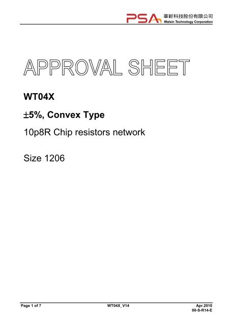
WT04X ±5%, Convex Type 10p8R Chip resistors network Size 1206
WT04X ±5%, Convex Type 10p8R Chip resistors network Size 1206
WT04X ±5%, Convex Type 10p8R Chip resistors network Size 1206

Create successful ePaper yourself
Turn your PDF publications into a flip-book with our unique Google optimized e-Paper software.
<strong>WT04X</strong><br />
±5%, <strong>Convex</strong> <strong>Type</strong><br />
<strong>10p8R</strong> <strong>Chip</strong> <strong>resistors</strong> <strong>network</strong><br />
<strong>Size</strong> <strong>1206</strong><br />
Page 1 of 7 <strong>WT04X</strong>_V14 Apr.2010<br />
00-S-R14-E
FEATURE<br />
1. Small size and light weight<br />
2. Reduced size of final equipment<br />
3. Lower surface mounted assembly costs<br />
4. Higher component and equipment reliability<br />
5. RoHS compliant and Lead free products<br />
APPLICATION<br />
• Consumer electrical equipment<br />
• EDP, Computer application<br />
DESCRIPTION<br />
The <strong>resistors</strong> array is constructed in a high grade ceramic body (aluminum oxide). Internal metal electrodes are<br />
added at each end and connected by a resistive paste that is applied to the top surface of the substrate. The<br />
composition of the paste is adjusted to give the approximate resistance required and the value is trimmed to<br />
within tolerance by laser cutting of this resistive layer.<br />
The resistive layer is covered with a protective coat. Finally, the two external end terminations are added. For<br />
ease of soldering the outer layer of these end terminations is Tin (Pb free) alloy.<br />
Fig 1. Consctruction of a <strong>Chip</strong>-R <strong>network</strong> <strong>WT04X</strong><br />
Page 2 of 7 <strong>WT04X</strong>_V14 Apr.2010<br />
00-S-R14-E
QUICK REFERENCE DATA<br />
Series No.<br />
Item<br />
General Specification<br />
<strong>WT04X</strong>(<strong>Convex</strong> type)<br />
<strong>Size</strong> <strong>1206</strong> (3216)<br />
Resistance Tolerance<br />
Resistance Range<br />
TCR (ppm/°C)<br />
Max. dissipation at T amb=70°C<br />
Max. Operation Voltage (DC or RMS)<br />
Max. overload voltage<br />
±5% (E24 series)<br />
10Ω ~ 100KΩ<br />
≤ ± 200 ppm/°C<br />
1/16 W<br />
Climatic category 55/155/56<br />
Note :<br />
1. This is the maximum voltage that may be continuously supplied to the resistor element, see “IEC publication<br />
60115-8”<br />
2. Max. Operation Voltage : So called RCWV (Rated Continuous Working Voltage) is determined by<br />
RCWV = Rated Power × Resistance Value or Max. RCWV listed above, whichever is lower.<br />
25V<br />
50V<br />
DIMENSIONS(unit : mm)<br />
<strong>WT04X</strong><br />
L 3.30 ± 0.20<br />
W 1.60 ± 0.15<br />
T 0.55 ± 0.10<br />
P 0.64 ± 0.05<br />
A 0.50 ± 0.05<br />
B 0.40 ± 0.15<br />
C 0.40 ± 0.15<br />
G 0.40 ± 0.15<br />
Page 3 of 7 <strong>WT04X</strong>_V14 Apr.2010<br />
00-S-R14-E
MARKING<br />
3-digits marking<br />
Each resistor is marked with a three digits code on the protective coating to designate the nominal resistance<br />
value. For values up to 9.1 the R is used as a decimal point. For values of 10.0 or greater the first 2 digits<br />
apply to the resistance value and third indicate the number of zeros to follow.<br />
Example<br />
RESISTANCE 10Ω 12Ω 100Ω 6800Ω 47000Ω<br />
3-digits marking 100 120 101 682 473<br />
FUNCTIONAL DESCRIPTION<br />
Product characterization<br />
Standard values of nominal resistance are taken from the E24 series for <strong>resistors</strong> with a tolerance of ±5%,<br />
The values of the E24 series are in accordance with “IEC publication 60063”<br />
Derating<br />
The power that the resistor can dissipate depends on the operating temperature; see Fig.2<br />
Figure 2. Maximum dissipation in percentage of rated power<br />
Circuit Mode<br />
As a function of the ambient temperature<br />
R1=R2=R3=R4=R6=R7=R8=R9<br />
Page 4 of 7 <strong>WT04X</strong>_V14 Apr.2010<br />
00-S-R14-E
MOUNTING<br />
Due to their rectangular shapes and small tolerances, Surface Mountable Resistors are suitable for handling by<br />
automatic placement systems.<br />
<strong>Chip</strong> placement can be on ceramic substrates and printed-circuit boards (PCBs).<br />
Electrical connection to the circuit is by individual soldering condition.<br />
The end terminations guarantee a reliable contact.<br />
SOLDERING CONDITION<br />
The robust construction of chip <strong>resistors</strong> allows<br />
them to be completely immersed in a solder<br />
bath of 260°C for 10 seconds. Therefore, it is<br />
possible to mount Surface Mount Resistors on<br />
one side of a PCB and other discrete<br />
components on the reverse (mixed PCBs).<br />
Surface Mount Resistors are tested for<br />
solderability at 235°C during 2 seconds. The<br />
test condition for no leaching is 260°C for 30<br />
seconds. Typical examples of soldering<br />
processes that provide reliable joints without<br />
any damage are given in Fig 3.<br />
Fig 3. Infrared soldering profile for <strong>Chip</strong> Resistors <strong>network</strong><br />
CATALOGUE NUMBERS<br />
The <strong>resistors</strong> have a catalogue number starting with .<br />
WT04 X 472_ J T L<br />
<strong>Size</strong> code<br />
WT04 : 0402<br />
per element<br />
<strong>Type</strong> code<br />
Reeled tape packaging<br />
X : 8 elements,<br />
convex<br />
terminations,<br />
common pin<br />
p5/p10<br />
Resistance code<br />
E24 : 2 significant digits followed<br />
by no. of zeros and a blank<br />
4.7Ω =4R7_<br />
10Ω<br />
220Ω<br />
Jumper<br />
=100_<br />
=221_<br />
=000_<br />
(“_” means a blank)<br />
: 8mm width paper taping 5000pcs per reel.<br />
Tolerance<br />
J : ±5%<br />
Packaging code<br />
T : 7” Reel taping<br />
Termination code<br />
L = Sn base (lead<br />
free)<br />
Page 5 of 7 <strong>WT04X</strong>_V14 Apr.2010<br />
00-S-R14-E
TEST AND REQUIREMENTS(JIS C 5201-1 : 1998)<br />
DC resistance<br />
Clause 4.5<br />
TEST PROCEDURE REQUIREMENT<br />
Temperature<br />
Coefficient of<br />
Resistance(T.C.R)<br />
Clause 4.8<br />
Short time overload<br />
(S.T.O.L)<br />
Clause 4.13<br />
Resistance to<br />
soldering heat(R.S.H)<br />
Clause 4.18<br />
Solderability<br />
Clause 4.17<br />
Temperature cycling<br />
Clause 4.19<br />
Load life (endurance)<br />
Clause 4.25<br />
Load life in Humidity<br />
Clause 4.24<br />
Adhesion<br />
Clause 4.32<br />
Insulation Resistance<br />
Clause 4.6<br />
Dielectric Withstand<br />
Voltage<br />
Clause 4.7<br />
DC resistance values measured at the test voltages specified<br />
below :<br />
PACKAGING<br />
Paper Tape specifications (unit :mm)<br />
Series No. A B W F E<br />
<strong>WT04X</strong> 3.45 +0.20/-0 1.85 +0.20/-0 8.00±0.30 3.50±0.20 1.75±0.10<br />
Series No. P1 P0 ΦD T<br />
<strong>WT04X</strong> 4.00±0.10 4.00±0.10<br />
+ 0.1<br />
Φ1.50<br />
− 0. 0 0.85±0.05<br />
Reel dimensions<br />
Symbol A B C D<br />
(unit : mm) Φ178.0±2.0 Φ60.0±1.0 13.0±0.2 9.0±0.5<br />
Page 7 of 7 <strong>WT04X</strong>_V14 Apr.2010<br />
00-S-R14-E