LED professional - Beriled
LED professional - Beriled
LED professional - Beriled

Create successful ePaper yourself
Turn your PDF publications into a flip-book with our unique Google optimized e-Paper software.
www.led-<strong>professional</strong>.com<br />
ISSN 1993-890X<br />
Review<br />
The technology of tomorrow for general lighting applications. May/June 2009 | Issue 13<br />
LpR<br />
<strong>LED</strong> Thermal<br />
Management<br />
Thermal Characterization<br />
Effect of Thermal<br />
Environment<br />
PowerPSoC Controller
Copyright © 2009 Luger Research & <strong>LED</strong>-<strong>professional</strong>. All rights reserved.<br />
“<strong>LED</strong>-FAIR”<br />
International:<br />
More Power –<br />
More Lumens<br />
Many companies in the lighting industry launched their new products<br />
at the Lightfair International in New York. It was a real demonstration<br />
of <strong>LED</strong> lighting; in fact a <strong>LED</strong>-Fair. Now, standard cool white <strong>LED</strong>s are<br />
available with more than 130 lm/W; the first commercially available<br />
quantum dot-<strong>LED</strong> lamp was introduced; a prototype of a 600lm<br />
dimmable <strong>LED</strong> bulb prototype for incandescent replacement was<br />
shown, and a downlight prototype showed more than 100lm/W fixture<br />
efficacy – only to name a few highlights.<br />
During the opening speech of the LIGHTFAIR International, Mr.<br />
Provoost, CEO of Philips Lighting, called upon the industry to work<br />
together on the adoption of standards for energy efficiency, along with open and collaborative<br />
innovation: “We call upon the lighting industry’s stakeholders to seize the tremendous opportunity<br />
to embrace the changes being brought about by a combination of government legislation and<br />
economic stimulus to build a sustainable future.”<br />
This is good news for the general lighting market based on high power <strong>LED</strong>s and packages,<br />
although Strategies Unlimited estimated that the High-Brightness-<strong>LED</strong> market will decrease by<br />
5% in 2009. The “green lighting” <strong>LED</strong> technology, without any toxic substances, is starting to<br />
replace classic lighting faster than expected. But one boundary still exists: the thermal impacts.<br />
The junction temperature of an <strong>LED</strong> is limited (e.g. 120°C) and besides the absolute limitations,<br />
temperature influencing parameters such as <strong>LED</strong> lifetime, lumen output, aging of epoxy materials,<br />
aging of electronic components (e.g. electrolytic capacitors) or color stability and quality, has to<br />
be carefully considered.<br />
Multiple approaches are available for developing, simulating and optimizing thermal management<br />
solutions for <strong>LED</strong> lighting systems. In general two cooling methods are used: the passive (material<br />
based) and the active ones. An active system needs an additional energy supply to operate, and<br />
hence these concepts reduce the system efficiency, to some extent, per definition. Nevertheless<br />
both kinds are important. Thermal simulation and dynamic tracing systems are state-of-the art.<br />
The aim is to spread the heat coming from the <strong>LED</strong>s, and conduct it through low thermal resistance<br />
transitions to the “environmental heat-sink.” The heat-sink-to-air junction is the most critical and<br />
different approaches, such as air jets, are being used today.<br />
The May/June 2009 <strong>LED</strong> <strong>professional</strong> Review (LpR) issue highlights <strong>LED</strong> Thermal Management and<br />
shows how to apply it to the <strong>LED</strong> technology in modern lighting systems.<br />
We would be delighted to receive your feedback about LpR or tell us how we can improve our<br />
services. You are also welcome to contribute your own editorials.<br />
Yours Sincerely,<br />
Siegfried Luger<br />
Publisher<br />
PS: New! The <strong>LED</strong> <strong>professional</strong> Review (LpR) package was upgraded with the bi-monthly <strong>LED</strong><br />
patent report and the “Hot News” information service. Have a look at the unique <strong>LED</strong> <strong>professional</strong><br />
membership services on www.led-<strong>professional</strong>-review.com.<br />
www.led-<strong>professional</strong>.com <strong>LED</strong> <strong>professional</strong> Review | May/June 2009 | page 1
Copyright © 2009 Luger Research & <strong>LED</strong>-<strong>professional</strong>. All rights reserved.<br />
Imprint<br />
<strong>LED</strong> <strong>professional</strong> Review (LpR)<br />
ISSN 1993-890X<br />
Publisher<br />
Luger Research e.U.<br />
Institute for Innovation & Technology<br />
dep <strong>LED</strong> <strong>professional</strong><br />
Faerbergasse 15, Haus Rot<br />
A 6850 Dornbirn, Austria / Europe<br />
phone +43 5572 394 489<br />
fax +43 5572 394 489 90<br />
editors@led-<strong>professional</strong>.com<br />
www.led-<strong>professional</strong>.com<br />
Publishing Editors<br />
Siegfried Luger<br />
Arno Grabher-Meyer<br />
Chrystyna Lucyk<br />
Account Manager<br />
Silvia Girardelli<br />
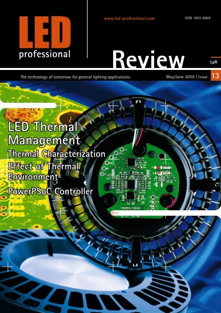
Front-page picture<br />
60W-PAR38 SynJet Cooler, Nuventix<br />
Artwork: Thomas Klobassa, ©<strong>LED</strong> <strong>professional</strong> 2009<br />
Copyrights – Luger Research e.U.<br />
The editors make every reasonable effort to verify the<br />
information published, but Luger Research e.U. assumes<br />
no responsibility for the validity of any manufacturers, non<br />
profit organisations or individuals claims or statements.<br />
Luger Research e.U. does not assume and hereby disclaims<br />
any liability to any person for any loss or damage caused<br />
by errors or omissions in the material contained herein,<br />
regardless of whether such errors result from negligence,<br />
accident or any other cause whatsoever. You may not copy,<br />
reproduce, republish, download, post, broadcast, transmit,<br />
make available to the public, or otherwise use of <strong>LED</strong><br />
<strong>professional</strong> Review (LpR) content without the prior written<br />
permission from Luger Research e.U. – Institute for<br />
Innovation & Technology, Austria.<br />
<strong>LED</strong> <strong>professional</strong> Review (LpR) -<br />
Annual Subsriptions<br />
LpR Digital Magazine<br />
• 6 issues<br />
• pdf download<br />
• high resolution pictures and graphs<br />
• printable<br />
• commercial use<br />
• access to all previous issues<br />
• bimonthly Patent Report<br />
• “Hot News” service<br />
• Euro 78.80<br />
• http://led-<strong>professional</strong>-review.com<br />
LpR Printed Magazine<br />
• 6 issues<br />
• Euro 158.40<br />
Next LpR Issue - July/Aug 2009<br />
• <strong>LED</strong> Light Generation<br />
www.led-<strong>professional</strong>.com <strong>LED</strong> <strong>professional</strong> Review | May/June 2009 | page 2
Copyright © 2009 Luger Research & <strong>LED</strong>-<strong>professional</strong>. All rights reserved.<br />
Content<br />
Advertising Index<br />
EVERLIGHT<br />
p C2<br />
Editorial<br />
Imprint<br />
Project News<br />
Product News<br />
Research News<br />
Announcements<br />
p1<br />
p2<br />
p5<br />
p6<br />
p13<br />
p13<br />
<strong>LED</strong> FORUM MOSCOW 2009 p 4<br />
CREE p 7<br />
ROHM EUROPE p 11<br />
MINLEON p 14<br />
OSRAM p 21<br />
EDISON p 31<br />
EURO<strong>LED</strong> 2009 p 37<br />
<strong>LED</strong>LIGHTFORYOU p 39<br />
Characterization<br />
Methodology for Thermal and Electrical Characterization of Large Area O<strong>LED</strong>s<br />
by A. Poppe et al, Budapest Univ. of Tech., Mentor Graphics, Philips Research Lab. p15<br />
On the Standardization of Thermal Characterization of <strong>LED</strong>s<br />
by A. Poppe et al, Budapest Univ. of Tech., Mentor Graphics, Philips Research Lab. p22<br />
Effect of Thermal Environment on <strong>LED</strong> Light Emission and Lifetime<br />
by Cathy Biber, Ph.D., Biber Thermal Design, Ltd<br />
p30<br />
CERAMTEC p 43<br />
MENTOR GRAPHICS p 43<br />
CIOE p 55<br />
LIGHT MIDDLE EAST<br />
p C3<br />
INTERNATIONAL RECTIFIER p C4<br />
Driver<br />
Advantages of Integrating Power and Control for <strong>LED</strong> Lighting Applications<br />
by Gavin Hesse and Rakesh Reddy, Cypress Semiconductor<br />
Constant Current Regulators Support <strong>LED</strong> Lighting Solutions<br />
by Tim Kaske, Paul Decloedt, ON Semiconductor<br />
p36<br />
p40<br />
Thermal Management<br />
Comparison of Passive and Active Cooling Effectiveness<br />
by Che Cheung, Brandon Noska and Kim van der Heide, Nuventix<br />
Thermal Management of High-Power <strong>LED</strong> Systems<br />
by Maurice J. Marongiu, PhD, MJM Engineering Co.<br />
Selecting the Right Thermal Interface Material for <strong>LED</strong> Applications<br />
by Robert Kranz, Dr. Richard Hill, Laird Technologies, Inc<br />
Thermal Management of Sophisticated <strong>LED</strong> Solutions<br />
by Dr. Michel Kazempoor, PerkinElmer<br />
Design Process for a Customer-Specific Ceramic Heat Sink<br />
by Rüdiger Herrmann, CeramTec AG<br />
p42<br />
p47<br />
p50<br />
p53<br />
p56<br />
<strong>LED</strong> <strong>professional</strong> – Patent Report<br />
p60<br />
www.led-<strong>professional</strong>.com <strong>LED</strong> <strong>professional</strong> Review | May/June 2009 | page 3
Copyright © 2009 Luger Research & <strong>LED</strong>-<strong>professional</strong>. All rights reserved.<br />
Project News<br />
<strong>LED</strong>s Replicate Golden Glow<br />
of Gas Lamps<br />
Historic gas street lamps in cities like Berlin, Prague and Warsaw can now<br />
be upgraded to energy-saving <strong>LED</strong> technology, thanks to a solid-state<br />
retrofit designed by Berlin-based Braun Schaltgeräte & Service with<br />
assistance from <strong>LED</strong> solutions provider Future Lighting Solutions. The first<br />
eight <strong>LED</strong> models were recently installed on Berlin’s Alexanderplatz public<br />
square, slashing power consumption by more than 90% without altering<br />
the old-world look or the light quality of the gas-driven fixtures.<br />
Lighting the Chinese Ancient<br />
Art at Da An Art Gallery<br />
Seoul Semiconductor Co., Ltd., a global <strong>LED</strong> maker, announced that<br />
their Z-Power <strong>LED</strong> P4 series products were used as the spotlights for<br />
the exhibits at Da An Art Gallery in Zhongshan City, Guangdong<br />
Province, China. The gallery required specific standards and needed<br />
high technological power and stability. The <strong>LED</strong> products are<br />
recognized for saving about 85% in energy consumption compared to<br />
halogen lamps and solves the problem of damaging the artwork<br />
through ultraviolet radiation.<br />
Seoul Semiconductor’s <strong>LED</strong>s lighted the ancient works of Chinese art.<br />
New <strong>LED</strong> module fits old gaslight form factor.<br />
Braun’s drop-in <strong>LED</strong> replacement modules replicate the distinctive golden<br />
glow of gas lighting with warm white LUXEON® Rebel <strong>LED</strong>s, providing a<br />
beam color that cannot be reproduced with cooler light sources like mercury<br />
vapor and sodium vapor. In addition to reducing energy bills, the <strong>LED</strong> lamps<br />
will last more than 50,000 hours compared to 4,000 for gas and an average<br />
16,000 for standard electrical illumination. They will also improve color<br />
rendering for better visibility of street signs and other objects.<br />
Engineers at Future Lighting Solutions, the exclusive supplier of LUXEON<br />
<strong>LED</strong>s, provided proof-of-concept and other technical support services<br />
including optical modeling to help Braun develop an <strong>LED</strong> retrofit that would<br />
use the same four screw base sockets as the incandescent mantles in the<br />
existing gas lamps. Future’s contributions included recommending an <strong>LED</strong><br />
layout that would match the brightness and light distribution of the gasilluminated<br />
street lights as closely as possible.<br />
Braun plans to market its ‘<strong>LED</strong> Gaslight’ throughout Europe, which has more<br />
than 100,000 gas lamps overall. The design already was rated #1 in a<br />
comparison of four vendors’ retrofit products for its near-perfect replication<br />
of the color, brightness and light distribution of the gas originals.<br />
The detailed case study is available for download from<br />
http://www.led-<strong>professional</strong>.com/content/view/1386/29/.<br />
Lighting for exhibition at a gallery or a museum requires optimal light<br />
sources to show the pieces at their best. While the existing halogen<br />
lamps and fluorescent lamps for galleries or museums require additional<br />
filters or caps to prevent ultraviolet radiation that may damage the<br />
exhibits, <strong>LED</strong> lighting without ultraviolet radiation does not need any<br />
additional devices.<br />
Seoul Semiconductor replaced 50W halogen lamps with their 7.2W<br />
spotlights at the sculpture and calligraphy frame parts at Da An Art<br />
Gallery, which is expected to result in energy savings of up to 85%.<br />
S42180 of Z-Power <strong>LED</strong> P4 series applied to those spotlights has the<br />
coloring rending index of 93, indicating a high level of natural expression<br />
of light colors, and high efficiency, which is optimal for the lighting of<br />
museums and galleries.<br />
Lamp Type <strong>LED</strong> Halogen Incandesc. Fluorescent<br />
UV Radiation No Yes(little) Yes(little) Yes<br />
Light<br />
Conversion 90% 5% 5% 40%<br />
Efficiency<br />
Average<br />
Lifespan<br />
About 50K<br />
hours<br />
About 2K<br />
hours<br />
About 1K<br />
hours<br />
About 8K<br />
hours<br />
Da An Art Gallery located in Zhongshan City, Guangdong Province, China,<br />
where the works of Jun Tien Lee, a famous calligrapher and sculptor in that<br />
city, are being exhibited. This museum is making efforts for eco-friendly<br />
operation such as replacing the halogen lamps and fluorescent lamps with<br />
<strong>LED</strong> which is an eco-friendly light source with high efficiency.<br />
www.led-<strong>professional</strong>.com <strong>LED</strong> <strong>professional</strong> Review | May/June 2009 | page 5
Copyright © 2009 Luger Research & <strong>LED</strong>-<strong>professional</strong>. All rights reserved.<br />
Product News<br />
Osram’s New Oslon SSL <strong>LED</strong> -<br />
The New Class of Light<br />
Small in size, big on performance – that is the new ultra-white Oslon<br />
SSL <strong>LED</strong> from OSRAM Opto Semiconductors. Its package measures just<br />
3 x 3mm but, in terms of luminous efficacy, the <strong>LED</strong> is among the greats<br />
with a typical value of 100lm/W. Its properties provide the basis for<br />
high application efficiency thanks to high efficacies even at high<br />
currents, simplified thermal management, high reliability and a beam<br />
angle of 80°. The <strong>LED</strong> provides light that is ideal for spotlights, desk<br />
lights and ceiling floodlights.<br />
achieves a typical efficiency of 75lm/W and a brightness of 85lm. And<br />
brightness is an impressive 155lm at an operating current of 700mA<br />
(warm white). The advantage here is that applications that demand high<br />
lighting levels can be completed with fewer <strong>LED</strong>s.<br />
Luminus Devices: New White<br />
PhlatLight <strong>LED</strong> Products for<br />
Lighting Applications<br />
Luminus Devices, Inc. recently introduced the CSM-360-W PhlatLight®<br />
<strong>LED</strong>, designed specifically for general lighting applications, and the SST-<br />
50 White PhlatLight® <strong>LED</strong>, the first 5.5W monolithic large-chip <strong>LED</strong> in a<br />
surface-mount (SMT) package. It is the newest in a series of white <strong>LED</strong>s<br />
designed specifically for general lighting applications.<br />
CSM-360 White PhlatLight <strong>LED</strong><br />
The CSM-360-W combines the benefits of large monolithic chips in a<br />
multi-chip configuration to deliver a Chip-on-Board <strong>LED</strong> package<br />
capable of delivering 6000lm. This new class of <strong>LED</strong>s enables a variety<br />
of lighting applications not previously possible with traditional <strong>LED</strong>s,<br />
and as a result fixture manufacturers are now able to target 10,000 lm<br />
and higher applications with as few as two PhlatLight <strong>LED</strong> packages.<br />
The new Oslon SSL can be used as a replacement for halogen lamps in spotlights, desk lights and reading lights<br />
and can also be used in retrofit applications.<br />
The new Oslon SSL <strong>LED</strong> is an <strong>LED</strong> in the 1W class and meets the<br />
requirements for use in general lighting. It is very small, reliable and<br />
efficient even at high currents and, thanks to its beam angle of 80°, it is<br />
ideal for injecting light into external lenses. “Its ability to handle high<br />
currents efficiently enables our customers to create particularly energyefficient<br />
and cost-saving lighting solutions. The Oslon <strong>LED</strong> therefore has<br />
all the attributes to become the ‘green’ light source of the future,” said Dr.<br />
Gunnar Moos, SSL Marketing Manager at OSRAM Opto Semiconductors.<br />
Its low thermal resistance of 7k/W simplifies thermal management. Its<br />
small size gives designers the flexibility to create extremely sophisticated<br />
solutions. If particularly strong light is needed, several light sources can<br />
be combined in a cluster. In addition to ultra-white (5700 to 6500K), the<br />
<strong>LED</strong> will be available this summer in neutral white and warm white. Its<br />
color temperature will range from 2700 to 4500K<br />
The Oslon SSL is manufactured using the latest chip technology, ensuring<br />
a high luminous efficacy. At an operating current of 350mA, this light<br />
source achieves a typical brightness of 110lm in ultra-white (5700 and<br />
6500K), with a maximum possible luminous flux of 130lm at present. At<br />
an operating current of 350mA and a color temperature of 3000K it<br />
“The CSM-360-W has a lumen output range that provides industryleading<br />
efficiency and delivers a new level of performance not previously<br />
realized in a single <strong>LED</strong> package,” said Chad Stalker, Director of Product<br />
Marketing and Business Development for the Lighting Business Group<br />
at Luminus Devices. “In addition to the PhlatLight <strong>LED</strong> benefits of<br />
simplified fixture design with fewer <strong>LED</strong>s and corresponding optics and<br />
drivers, the CSM-360-W also provides a package platform making it<br />
possible to service and upgrade the <strong>LED</strong> itself instead of replacing the<br />
whole fixture.”<br />
The CSM-360-W is unique in several ways. It consists of four separate<br />
monolithic chips, each with a light-emitting surface of nine square<br />
millimeters in size, closely packed in a single Chip-on-Board package.<br />
The CSM-360-W produces over 3600lm at high efficacy and over 6,000<br />
lm at high output. PhlatLight <strong>LED</strong>s are mercury-free, highly reliable and<br />
provide a lifetime of 60000 hours with lumen maintenance of greater<br />
than 70%.<br />
SST-50 White PhlatLight <strong>LED</strong><br />
Luminus Devices, Inc. further announced the introduction of the SST-<br />
50 White PhlatLight® <strong>LED</strong>, the first 5,5W monolithic large-chip <strong>LED</strong> in a<br />
surface-mount (SMT) package. The SST-50 is designed to integrate<br />
directly with existing <strong>LED</strong> layouts and enable the next level of<br />
performance required by fixture designers to deliver <strong>LED</strong>-based<br />
solutions for mainstream applications in the general, architectural and<br />
portable lighting markets.<br />
www.led-<strong>professional</strong>.com <strong>LED</strong> <strong>professional</strong> Review | May/June 2009 | page 6
Copyright © 2009 Luger Research & <strong>LED</strong>-<strong>professional</strong>. All rights reserved.<br />
“In a direct response to the growing needs of lighting fixture designers,<br />
the SST-50-W PhlatLight <strong>LED</strong> offers a drop-in compatible SMT <strong>LED</strong> to<br />
existing, lower-power emitters,” Stalker described. “It enables lighting<br />
fixture designers and manufacturers to simplify designs by reducing<br />
the number of <strong>LED</strong>s in the system while maintaining high performance<br />
levels. Additionally, fixture manufacturers can easily increase light<br />
output of existing designs by a factor of two by simply replacing the<br />
current <strong>LED</strong>s with the new, higher-output SST-50-W PhlatLight <strong>LED</strong>.”<br />
New CETUS <strong>LED</strong> modules, e.g. C6060E, now have clearly increased efficacy.<br />
The SST-50 is the most recent member of the SST-<strong>LED</strong> series for lighting applications.<br />
The light-emitting surface of the SST-50-W white PhlatLight <strong>LED</strong> is a<br />
single, monolithic chip that is five square millimeters in size. The SST-<br />
50-W produces 550 lumens at 5.5W (100LPW at 6500K CCT) and<br />
upwards of 1250 lumens at its maximum rated drive current. Available<br />
in an SMT package, the SST-50-W integrates seamlessly with standard<br />
SMT manufacturing process and equipment. This series of PhlatLights<br />
are also mercury-free, highly reliable and provide a lifetime of 60000<br />
hours with lumen maintenance of greater than 70 percent. The SST-<br />
50-W is ideally suited for a variety of applications including portable<br />
lighting and general lighting as well as architectural lighting where high<br />
performance and high efficacy in a standard package is needed.<br />
Cetus E-Series Demonstrates<br />
Industry-Leading Efficacy<br />
Intematix Corp., a leading innovator in phosphors, <strong>LED</strong> components and<br />
solid state lighting modules announced the release of a new series of<br />
high-efficiency power <strong>LED</strong>s. The new Cetus “E-series” products boast<br />
efficacies of up to 100lm/W for the cool white versions, and 97lm/W<br />
for warm white, and will facilitate wider adoption of <strong>LED</strong>s in general and<br />
outdoor lighting. All models feature Intematix’s advanced phosphor<br />
technology, providing a high-efficacy and low-cost combination that<br />
addresses the key needs of luminaire designers.<br />
The standard CRI version of the E-series offers a combination of highlumen<br />
output and cost-effectiveness that is particularly attractive to<br />
outdoor lighting manufacturers, all of whom are striving for <strong>LED</strong><br />
luminaires that are both attractively priced and efficient in operation.<br />
The higher CRI models, due in June, will extend the range to include<br />
interior and architectural general lighting applications. Available<br />
standard CRI models include:<br />
• The C6060E high-flux model rated at 700mA drive current, achieving<br />
190lm typical in cool white, 185lm typical in warm white per <strong>LED</strong>.<br />
• The C5050E 1W <strong>LED</strong> with maximum cost-effectiveness, delivering<br />
100lm typical in cool white and 97lm in warm white. Its 10V forwardvoltage<br />
(Vf) specification is ideal for direct drive 12V applications<br />
such as landscape lighting.<br />
• The C7676E, a 1W to 2W, 100lm/W <strong>LED</strong> with a 51V f<br />
specification<br />
simplifies 110/220V direct drive applications.<br />
According to Intematix’s Director of Marketing, Ilkan Cokgor, “Wide<br />
area and outdoor lighting are applications where <strong>LED</strong>s outperform<br />
the incumbent technologies in lifetime, maintainability and energy<br />
costs, while generating much higher quality light. The continuing<br />
challenge has been the initial acquisition costs of current outdoor<br />
luminaires, which has negatively impacted payback periods.<br />
Intematix’s Cetus E-series sets a new benchmark for lumens per<br />
dollar, which will enable our customers to lower their costs and<br />
enhance ROI for their end-users.”<br />
Intematix’s high-quality chip-on-ceramic <strong>LED</strong>s are characterized by<br />
excellent heat management and luminous efficiency enabled by<br />
Intematix’s well-recognized patent-backed phosphor technologies.<br />
The Cetus E-series <strong>LED</strong>s are available in 5000K and 4000K cool<br />
white, or 3000K and 2700K warm white. Standard CRI versions of all<br />
models are available now, while versions with CRIs greater than 80<br />
are scheduled for production availability in June.<br />
www.led-<strong>professional</strong>.com <strong>LED</strong> <strong>professional</strong> Review | May/June 2009 | page 8
Copyright © 2009 Luger Research & <strong>LED</strong>-<strong>professional</strong>. All rights reserved.<br />
“The ability to offer high efficiency, cost effectiveness, and a range of<br />
colour temperatures carries little market impact without being able to<br />
back that up with product consistency,” commented Intematix’s Chief<br />
Technical Officer, Dr. Yi-Qun Li. “While the full Cetus line uses ANSI<br />
standard bins, our specific binning process assures customers will receive<br />
superior colour and brightness uniformity both within a shipment and<br />
from shipment-to-shipment.”<br />
Philips Lighting: 600 Lumen<br />
Dimmable <strong>LED</strong> Bulb<br />
Prototype for Retrofit<br />
Philips Lighting used the prestigious backdrop of the 2009 LIGHTFAIR<br />
International Trade Show & Conference in New York City to unveil its<br />
breakthrough and state-of-the-art new SSL solution: a record 600<br />
lumen output A-shaped <strong>LED</strong> bulb that can ultimately be used to<br />
replace 40W incandescent bulbs in general lighting applications in<br />
the U.S. market and 60W incandescent technology in the European<br />
(230V) market.<br />
Powerful, highly efficient, and fully dimmable down to 10%, Philips<br />
Lighting’s “next-generation” A-shape SSL, pre-production prototype<br />
bulb delivers a high-performing package of lumen output, lumen<br />
per watt efficacy, color, and dimmability that is currently unparalleled<br />
in the industry -- demonstrating Philips’ continued leadership in<br />
defining the future of lighting.<br />
The successor of the current Master-<strong>LED</strong> bulb achieves a record 600 lumen output.<br />
Powered Rebel <strong>LED</strong>s from Philips Lumileds, the 8 Watt by highperforming<br />
LUXEON 120V bulb delivers 75lm/W, which is five times the<br />
efficacy of an equivalent incandescent bulb. The bulb is fully dimmable<br />
down to 10% and is ideal for use in table lamps, overhead fixtures, and<br />
other indoor general lighting applications.<br />
Often described as the “future of lighting,” <strong>LED</strong> technology offers the<br />
benefits of bright color, outstanding energy efficiency, long life, and<br />
minimal maintenance. With this breakthrough dimmable A-shape bulb<br />
from Philips, lighting users worldwide will enjoy a high-quality <strong>LED</strong><br />
replacement for incandescent bulbs that delivers comfortable and<br />
controllable light for their broad range of general lighting applications<br />
while significantly reducing energy consumption and costs and greatly<br />
enhancing environmental sustainability.<br />
“As leaders in the development and promotion of solid state lighting<br />
(SSL) platforms, Philips is very excited to break new ground in the SSL<br />
arena and to introduce revolutionary product concepts and executions<br />
to lighting users worldwide,” says Guido van Tartwijk, head of Philips<br />
Lighting’s Global Product Marketing division for <strong>LED</strong> Retrofit. “Philips’<br />
new A-shape dimmable SSL bulb represents a global breakthrough and<br />
game-changing solution that will truly help deliver paradigm<br />
transformations around the world, enabling lighting users to capitalize<br />
on their energy-efficient SSL retrofit opportunities and explore the vast<br />
possibilities of light.”<br />
Nexxus Lighting & QD<br />
Vision: Quantum Dot-<strong>LED</strong><br />
Lamp Line<br />
The first commercial lamp that integrates quantum dot technology to<br />
be demonstrated at Lightfair 2009 are a breakthrough technology that<br />
combines warm, rich color with <strong>LED</strong> efficiency, providing 2700K, 90+<br />
CRI at 65 Lumens Per Watt.<br />
Nexxus Lighting, Inc. (NASDAQ Capital Market: NEXS) and QD Vision,<br />
Inc. unveiled the world’s first quantum dot lighting solution that<br />
combines the efficiency of <strong>LED</strong> lighting with the warm color of<br />
incandescent bulbs. The new lamp integrates a quantum dot optic with<br />
cool white <strong>LED</strong>’s to produce color-rich, true incandescent, warm white<br />
light which can provide over 80% energy savings and lasts up to 25<br />
times longer than comparable halogen lighting alternatives.<br />
Architects and the lighting design community have been demanding a<br />
higher CRI <strong>LED</strong> product without the efficacy losses typically associated<br />
with these lamps. The new Quantum Light optic developed by QD<br />
Vision, integrated with Nexxus Lighting’s patented Array Lamp designs<br />
and patent pending technology, solves this critical issue. The Nexxus<br />
Lighting Array TM lamp with the Quantum Light TM optic delivers a true<br />
incandescent, warm white, 2700 degree Kelvin lamp with a color<br />
rendering index of 90 or greater at over 65 lumens per watt<br />
The companies demonstrated the product and technology at Lightfair<br />
International 2009 at the Javits Center in New York, May 5 - 7, 2009.<br />
The Array Lighting Quantum Light solution for all Nexxus Lighting<br />
Array Par 30, MR 16 and Par 16 lamps is expected to be available in the<br />
4 th quarter of 2009, with volume production in early 2010.<br />
www.led-<strong>professional</strong>.com <strong>LED</strong> <strong>professional</strong> Review | May/June 2009 | page 9
Copyright © 2009 Luger Research & <strong>LED</strong>-<strong>professional</strong>. All rights reserved.<br />
The Array Lighting Quantum Light solution will be used for all Nexxus Lighting lamps.<br />
Cree: Brightest and Highest-<br />
Efficiency Lighting-Class <strong>LED</strong><br />
and Prototype <strong>LED</strong> Downlight<br />
Cree, Inc., a market leader in <strong>LED</strong> lighting, demonstrated the newest<br />
addition to its lighting-class XLamp(r) <strong>LED</strong> family - the XLamp XP-G<br />
<strong>LED</strong> - at LIGHTFAIR International in New York, May 5-7, 2009.<br />
The cool white XLamp XP-G provides 139lm/W and 132lm/W at 350mA.<br />
Driven at 1A, the XP-G produces 345lm, which is 37% brighter and 53%<br />
more efficient than the brightest XR-E <strong>LED</strong>. The XP-G <strong>LED</strong> has the<br />
highest lumen density of any available lighting-class <strong>LED</strong>, and it is based<br />
on the XLamp XP family package.<br />
“Nexxus Lighting’s new Array <strong>LED</strong> lamp line is a perfect application for<br />
our quantum dot technology,“ said Dan Button, President and CEO of<br />
QD Vision. “This productive partnership, combining QD Vision’s Quantum<br />
Light optic and the leading design capabilities of Nexxus Lighting, has<br />
resulted in a product the market has long been demanding – lamps with<br />
exceptional color quality and power efficiency together.”<br />
“We are excited to add this new high color rendering, true incandescent<br />
warm white color choice to our successful Array <strong>LED</strong> lamp product<br />
offering”, stated Mike Bauer, President and CEO of Nexxus Lighting.<br />
“The architectural lighting community has been clear in its demand for<br />
better color rendering performance in <strong>LED</strong> lighting, without sacrificing<br />
the efficacy gains you can achieve through solid state solutions.”<br />
The product resulting from the Nexxus Lighting/QD Vision partnership<br />
was recently demonstrated at a White House ceremony, in which<br />
President Obama announced a $1,6 billion disbursement of research<br />
funds for clean energy products. The Nexxus Lighting/QD Vision project<br />
was one of only four technologies spun out of MIT that were<br />
demonstrated at the event, which featured remarks by MIT President<br />
Susan Hockfield.<br />
Because the Nexxus Lighting Array lamps with Quantum Light TM are<br />
compatible with a standard, screw-in ‘Edison’ base, they can easily<br />
replace incandescent and halogen lamps in existing downlight fixtures.<br />
Just in the US, the DoE estimates, the number of down lights and track<br />
heads with Edison base lamp installations equal over 139 million in<br />
commercial applications and over 262 million in residential lighting<br />
applications. Both companies expect that commercial availability of<br />
their high efficiency lamps with high color quality will overcome a major<br />
barrier to <strong>LED</strong>s and will accelerate the penetration of <strong>LED</strong>s in the $4<br />
billion U.S. lamp market. The potential impact on the environment could<br />
be significant, a full conversion to <strong>LED</strong>s of existing downlights and<br />
trackheads in the US (~10% of US fixtures) represents an annual savings<br />
of more than 35 billion KW hours (nearly $4 billion), which is the<br />
equivalent of nearly 6 power plants or more than 60 million barrels of<br />
oil per year.<br />
The high-efficiency LR6 prototype features TrueWhite TM technology, resulting in a 92 color rendering index and a<br />
3500K color temperature by using the latest Cree <strong>LED</strong>s, the XLamp® XP-G.<br />
“The XLamp XP-G again raises the level of performance available from<br />
our XLamp <strong>LED</strong> family,” said Paul Thieken, Cree’s Marketing Director of<br />
<strong>LED</strong> components. “This product is designed for customers requiring the<br />
highest levels of brightness and efficacy.”<br />
The XLamp XP-G <strong>LED</strong> was demonstrated at Cree’s LIGHTFAIR International<br />
Booth. Cree is currently taking sample requests for the XLamp XP-G<br />
and targets the product to be commercially available the third quarter<br />
of calendar year 2009.<br />
Building on its leadership in <strong>LED</strong> lighting, Cree announces it is<br />
demonstrating a prototype version of the LR6 <strong>LED</strong> recessed downlight<br />
that consumes just 6.5W of electricity, resulting in 665lm, an efficacy<br />
of 102lm/W and a power factor greater than 0.9.<br />
“By using the latest Cree <strong>LED</strong>s, the XLamp® XP-G, we were able to<br />
achieve this great efficiency,” said Gerry Negley, chief technologist for<br />
Cree <strong>LED</strong> Lighting. “We continue to push the envelope with <strong>LED</strong><br />
technology — because consumers deserve high-quality light without<br />
toxic mercury or wasted energy.”<br />
www.led-<strong>professional</strong>.com <strong>LED</strong> <strong>professional</strong> Review | May/June 2009 | page 10
Copyright © 2009 Luger Research & <strong>LED</strong>-<strong>professional</strong>. All rights reserved.<br />
ROHM Semiconductor:<br />
Ambient Light Sensor<br />
ROHM Semiconductor announces a new family of analog and digital<br />
Ambient Light Sensor (ALS) ICs. These ALS ICs are ideal for a multitude<br />
of portable electronic products such as mobile phones, digital cameras,<br />
PDAs, notebooks a.o., requiring enhanced visibility, independent of a<br />
wide range of illumination conditions as well as optimized power<br />
consumption.<br />
Featuring ROHM’s proprietary trimming process and use of multiple<br />
photodiodes with different junction depths, they provide an accurate<br />
output with only little variation between various light sources. The<br />
spectral response of ROHM ALS ICs has been tailored to closely match<br />
that of the human eye for accurate light measurement. These features<br />
combine to provide uniform visibility for LCDs over a wide range of<br />
ambient light levels and sources – from incandescent or fluorescent<br />
light to full sunlight.<br />
BH16xx analog series devices provide a linear current output proportional<br />
to luminous intensity ranging from 0 to 100000 lux. These units feature<br />
ROHM’s unique three-level gain selection providing exceptional design<br />
flexibility in matching power consumption to the specific application<br />
requirements.<br />
The BH17xx series of digital devices integrate a 16-bit analog-to-digital<br />
converter that produces 1lx resolution over a range of 0 to 60000lx. The<br />
devices’ I 2 C output is designed for direct connection to a microcontroller<br />
or baseband processor. Two measurement resolution levels are provided<br />
allowing design trade-offs between sampling time and performance.<br />
For example, with high-resolution sampling, optical noise such as<br />
fluorescent lamp flicker can be filtered out. Low resolution provides a<br />
shorter sampling time for applications such as GPS systems where the<br />
light level changes are dynamic.<br />
Key advantages of the ROHM ALS Series include:<br />
• Higher light-sensing accuracy (±15% compared to competitive<br />
devices that range from ±30% to ±55%).<br />
• More stable ambient light detection (±10% maximum difference<br />
regardless of light source, compared to competitive products with up<br />
to 4:1 variations).<br />
• Wide operating temperature range (-40ºC to 85ºC).<br />
• Wide light detection range (up to 100000 lux).<br />
• Small, surface-mount packaging.<br />
• RoHS-compliant and halogen-free package.<br />
• Optimized power consumption (e.g. reducing up to 30% of the power<br />
in standby mode).<br />
Günter Richard said: “Adjusting the <strong>LED</strong> backlight intensity to compensate<br />
for varying light levels can save 50% or more of the total power required<br />
to operate many LCD-equipped devices. The ROHM family of analog and<br />
digital ALS ICs offers an exceptional range of performance capabilities for<br />
the full scale of <strong>LED</strong> backlighting applications.”<br />
www.led-<strong>professional</strong>.com <strong>LED</strong> <strong>professional</strong> Review | May/June 2009 | page 11
Copyright © 2009 Luger Research & <strong>LED</strong>-<strong>professional</strong>. All rights reserved.<br />
Philips Presents World’s First<br />
O<strong>LED</strong>-Based Interactive<br />
Lighting Concepts<br />
Royal Philips Electronics premiered the world’s first O<strong>LED</strong> (Organic Light-<br />
Emitting Diodes) -based interactive lighting concepts, created for both<br />
consumer as well as <strong>professional</strong> use, during the Euroluce International<br />
Lighting Fair in Milan. The concepts are intuitive and interactive in use,<br />
boast ultra flat shapes, soft light-effects and design possibilities never<br />
before seen in lighting products. The result is lighting that goes beyond<br />
mere illumination – it becomes an experience in itself.<br />
The concepts are the culmination of years of research that have placed<br />
Philips at the cutting edge of solid-state lighting. “In addition to our<br />
expertise in <strong>LED</strong>s, we are now unlocking the great potential of flat,<br />
energy-efficient O<strong>LED</strong>s,” says Rudy Provoost, CEO of Philips Lighting.<br />
Our concepts demonstrate a new light ambiance, novel design<br />
possibilities and unique interactivity of light and human gesture.”<br />
For homes, Philips is presenting four different concepts: standing, wallmounted,<br />
desk-top and ceiling luminaires. All incorporate glowingly<br />
radiant flat O<strong>LED</strong> light panels, supplemented with LUXEON Power <strong>LED</strong>s<br />
for the functional lighting part. Each model has different intuitive<br />
interactive capabilities. The ceiling concept, for example, features a<br />
balance of up-light and down-light that can be changed or dimmed to<br />
alter the ambience in a room with a gesture of the hand. All of the<br />
concepts on show share a sleek, streamlined design that makes them as<br />
decorative as they are functional.<br />
“The global lighting industry is in a state of great transition,” continued<br />
Rudy Provoost. “Economic and environmental concerns are driving all<br />
of us to make the move from incandescent lamps to cleaner, more<br />
energy-efficient solutions as quickly as we can. The solid state lighting<br />
revolution is happening at the right time. What’s particularly exciting is<br />
that <strong>LED</strong>s and O<strong>LED</strong>s offer the possibility to create new lighting designs<br />
and experiences that weren’t achievable in the past. With these new<br />
concepts Philips is adding a whole new dimension to lighting and the<br />
way it can enhance people’s lives.”<br />
ERG Offers <strong>LED</strong> Drivers for<br />
SSL Luminaires<br />
Illumination power and control specialist Endicott Research Group<br />
(ERG) is developing new <strong>LED</strong> driver solutions for the solid state lighting<br />
(SSL) market. Leveraging technology developed for its CCFL inverters<br />
and <strong>LED</strong> backlight drivers, ERG will be introducing a family of Smart<br />
Force <strong>LED</strong> drivers that combine full-function power supplies with<br />
energy-efficient controllers for commercial, industrial, architectural<br />
and other SSL applications.<br />
ERG’s Smart Force SSL drivers will offer 1-200W unit power for driving<br />
single or multiple <strong>LED</strong> strings.<br />
Philips (O<strong>LED</strong> Chandelier and O<strong>LED</strong> Tabletop) presenting four different concepts: standing, wall-mounted, desktop<br />
and ceiling luminaires.<br />
Philips is also unveiling an O<strong>LED</strong> installation for <strong>professional</strong> segments in<br />
large spaces, such as reception areas. As in the case of the consumer<br />
concepts, this installation is both functional and highly experiential,<br />
featuring a luminescent wall that reacts directly to passers-by, creating<br />
mirrored reflections of their ‘shadows’ amid the light. Philips invites “play”<br />
with this new technology and an experience that is much more than just<br />
light: a softly glowing mirror, an interactive tool, a very aesthetic light<br />
source and an inspiration for further products and applications.<br />
ERG’s Smart Force SSL drivers with vacuum encapsulation are so well insulated from the elements that they can<br />
light an <strong>LED</strong> string while literally under water.<br />
Standard features include:<br />
• Universal input (85-277V at 50Hz or 60Hz).<br />
• Power factor correction of 0,9 or better to maximize circuit efficiency<br />
and minimize power consumption.<br />
• Constant current with extremely low ripple to eliminate thermal<br />
issues and visible artifacts.<br />
• High efficiency (90%) to help luminaires meet ENERGY STAR ratings.<br />
• MTBF of more than 50000 hours.<br />
• 3-Year warranty.<br />
www.led-<strong>professional</strong>.com <strong>LED</strong> <strong>professional</strong> Review | May/June 2009 | page 12
Copyright © 2009 Luger Research & <strong>LED</strong>-<strong>professional</strong>. All rights reserved.<br />
Additional features to be available include triac dimming, color<br />
temperature regulation, ambient light control and vacuum encapsulation<br />
for added durability (a technique unique to ERG). IP67, UL1310 Class 2<br />
and other key regulatory approvals are pending. The drivers will be<br />
available as a standard off-the shelf product or in custom designs. ERG<br />
will maintain a full in-house engineering staff at its U.S. headquarters<br />
to meet virtually any special application requirement.<br />
Research News<br />
Japanese Researchers Double<br />
Green Phosphorescent O<strong>LED</strong><br />
Efficiency<br />
A Japanese research group succeeded in making an O<strong>LED</strong> device using<br />
a green light-emitting phosphor material and achieving a very high<br />
light-emitting efficiency of 210lm/W.<br />
When emitting light at a luminance of 10cd/m2, it has a light-emitting<br />
efficiency of 210lm/W and a light-extraction efficiency of 56,9%. On<br />
the other hand, when emitting light without the high-refractive glass<br />
plate, its light-emitting efficiency is only 94,3lm/W. This means the<br />
glass plate boosted the light-extraction efficiency by 2,3 times.<br />
Developed through detailed theoretical analysis<br />
The research group made the achievement by developing “FRO<strong>LED</strong>”<br />
software that theoretically calculates optical behaviors, and by “conducting<br />
a detailed analysis on light-extraction efficiency for the first time in<br />
Japan,” Mikami said.<br />
The glass plate results in higher light-extraction efficiency because, “the<br />
high-refractive glass plate strongly attracts the optical energy, which<br />
usually remains inside the thin film and the substrate of an O<strong>LED</strong> at a ratio<br />
of about 1:1, to the side of the substrate,” Mikami said. And the lens array<br />
structure formed on the surface of the glass plate enables to extract light<br />
that is otherwise trapped in the substrate and the glass plate, he further<br />
explained.<br />
“The light-extraction efficiency is theoretically calculated to be 75%,<br />
which is three times higher than before,” Mikami declared. “We might be<br />
able to realize it by improving the device manufacturing technology.”<br />
Announcements<br />
The high-efficiency, green light-emitting O<strong>LED</strong> device developed<br />
by the Mikami Lab at the Kanazawa Institute of Technology.<br />
The research group, which is led by Professor Akiyoshi Mikami of the<br />
Advanced Optical Electro Magnetic Field Science Lab, the Kanazawa<br />
Institute of Technology, boosted the light-extraction efficiency to<br />
56.9%, more than twice that of existing O<strong>LED</strong> devices. The group made<br />
this announcement at the JSAP (Japan Society of Applied Physics) 56 th<br />
Spring Meeting, 2009, which took place at Tsukuba University in Japan,<br />
from March 30 to April 2, 2009.<br />
It has been regarded as a big challenge for O<strong>LED</strong> devices to enhance<br />
their low light-extraction efficiency of slightly less than 30%. Using the<br />
new technology, it is possible that the light-emitting efficiencies of<br />
O<strong>LED</strong> displays and lamps will sharply increase.<br />
The O<strong>LED</strong> device developed by the research group has the bottom<br />
emission type structure, which extracts light through a substrate made<br />
with transparent electrodes. In addition, a 0,7mm-thick glass plate with<br />
a refraction index as high as 2,03 is bonded to the substrate. The surface<br />
of this glass plate is processed to have a structure of about 0,3mmpitch<br />
optical lens array.<br />
The material for the device’s light-emitting layer is a host material called<br />
“CBP” added with an iridium complex, “Ir(ppy)3.” Its light emission peak<br />
lies in the range of wavelengths between 500 and 550nm, which<br />
corresponds to green color.<br />
<strong>LED</strong> FORUM MOSCOW 2009<br />
Speaking opportunities and market overview<br />
The INTERNATIONAL <strong>LED</strong> FORUM “<strong>LED</strong>s in Lighting Technologies“<br />
(November 11-12 th , Moscow) is the most important <strong>LED</strong> conference in<br />
Eastern Europe/Russia. No other event offers a better overview over<br />
developments of the Eastern European and Russian markets for <strong>LED</strong><br />
technologies. It is the ideal platform for international companies to<br />
analyze the Russian market, meet new clients and to initiate business<br />
contacts with potential distributors.<br />
Russia’s demand for <strong>LED</strong> lighting technologies will increase, as Russian<br />
authorities promote <strong>LED</strong> technologies in accordance with the energy<br />
efficiency program of the Russian state. This year’s <strong>LED</strong> FORUM is<br />
dedicated to the topic “<strong>LED</strong> technologies: A new quality of lighting”. The<br />
second day casts a light on “Shop lighting with <strong>LED</strong>”, “Outdoor and<br />
indoor lighting with <strong>LED</strong>” and the ever more important topic of “Lighting<br />
control systems and <strong>LED</strong>s”.<br />
If you are interested in making a contribution to the <strong>LED</strong> FORUM<br />
MOSCOW, please contact:<br />
Eugene Dolin, President of the OrgCommittee +7 985 290 60 90<br />
or Angelika Meier, Conference Manager +49 9122 830502<br />
Further information: www.ledforum-moscow.com.<br />
www.led-<strong>professional</strong>.com <strong>LED</strong> <strong>professional</strong> Review | May/June 2009 | page 13
Copyright © 2009 Luger Research & <strong>LED</strong>-<strong>professional</strong>. All rights reserved.<br />
Companies Invited to Respond<br />
to Prior Information Notice<br />
SMART SPP – innovation through sustainable procurement is a European<br />
project which will promote the introduction of new, innovative low<br />
carbon emission technologies and integrated solutions onto the<br />
European market. This will be done by encouraging early market<br />
engagement between public authority procurers and suppliers and<br />
developers of new innovative products and services in the preprocurement<br />
phase of public tenders.<br />
The project is supported by the Intelligent Energy Europe funding<br />
programme. It is a multi-partner initiative which involves experts from<br />
organisations across Europe. Further information on these organisations<br />
is available on the Partners page.<br />
SMART SPP will develop a standard approach to pre-procurement of<br />
emerging technologies. The approach will include managing the risks in<br />
pre-procurement, assessing the financial benefits (life-cycle costing),<br />
and calculating and communicating the C0 2<br />
savings.<br />
Prior to the development of the standard approach, a needs analysis<br />
will be conducted to ensure the outcomes of the project are as useful<br />
as possible to public authorities and their suppliers. In addition, existing<br />
best practice in the field of pre-procurement, legal considerations and<br />
appropriate solutions, technologies and suppliers to involve in the<br />
project will be explored.<br />
Tools, tender documents, manuals and training sessions will also be<br />
developed to assist in building the capacity of public authorities who<br />
wish to use pre-procurement to purchase emerging technologies.<br />
Now the European project SMART SPP has issued a Prior Information<br />
Notice (PIN). It is available online at<br />
http://ted.europa.eu/udluri=TED:NOTICE:112139-2009:TEXT:EN:HTML.<br />
Interested suppliers and manufacturers of innovative highly energy<br />
efficient technologies are invited to contact the issuer of the PIN to<br />
register their interest in participating in the next stage i.e. market<br />
engagement. Technologies in focus include:<br />
• <strong>LED</strong> solutions for traffic lights, <strong>LED</strong> solutions for street lighting and<br />
(O)<strong>LED</strong> solutions for office lighting, including retrofitting solutions.<br />
• Full EV solutions, including passenger cars and duty vehicles used in<br />
public authorities as well as complete system solutions, including<br />
plug-in EV and refilling stations.<br />
• RES heating cooling solutions, including solar adsorption chiller for<br />
municipal buildings and other technology solutions currently in the<br />
end R&D phases.<br />
• Solid State Technology based ICT equipment.<br />
Furthermore, the first SMART SPP technical report “Existing approaches<br />
to encourage innovation through procurement” has been published,<br />
reviewing early market engagement, risk management, life cycle costing<br />
and CO 2<br />
eq monitoring tools and approaches, and concluding how best<br />
to drive innovation through sustainable procurement.<br />
Information on SMART SPP is available online at www.smart-spp.eu.<br />
www.led-<strong>professional</strong>.com <strong>LED</strong> <strong>professional</strong> Review | May/June 2009 | page 14
Copyright © 2009 Luger Research & <strong>LED</strong>-<strong>professional</strong>. All rights reserved.<br />
Characterization<br />
Methodology for Thermal and<br />
Electrical Characterization of<br />
Large Area O<strong>LED</strong>s<br />
> A. Poppe et al, Budapest University of Technology (BME),<br />
Mentor Graphics MicReD Division, Philips Research Laboratories<br />
Research until now has mainly been motivated by glass-based organic<br />
electroluminescence (O<strong>LED</strong> - Organic Light Emitting Diode) displays [1],<br />
where the aspects of increased contrast, high viewing angle and response<br />
speed are critical. With the increasing luminance and efficiency of O<strong>LED</strong>s<br />
intelligent lighting applications are becoming increasingly relevant. In the<br />
research project called Fast2Light [2] the overall objective is to develop a<br />
novel, cost-effective, high-throughput, roll-to-roll, large area deposition<br />
process for fabricating light-emitting polymer-O<strong>LED</strong> foils for intelligent<br />
lighting applications.<br />
Lighting purpose O<strong>LED</strong>s require high power density, however the polymer<br />
substrate and the materials used in the devices have bad electrical and<br />
heat transfer properties. In this article simulation and measurement<br />
results on some sample O<strong>LED</strong>s will be presented and new electro-thermal<br />
extension of the SUNRED field solver program [3] are introduced.<br />
Organic Light Emitting Devices<br />
Although conventional <strong>LED</strong>s based on III-V semiconductors (AlInGaP,<br />
InGaN) achieve bright emission with sufficient quantum efficiency for the<br />
visible spectral region, their use for flat panel displays or large area general<br />
lighting applications is unlikely due to the fabrication cost and packaging<br />
issues. Organic semiconductors, however, show good charge carrier<br />
transport properties as well as are excellent candidates for cheap and<br />
highly effective alternatives for large area applications [4].<br />
transparent to light [5]. Voltage bias is applied on the electrodes. The<br />
voltages are low, from 2.5 to ~ 20V, but the active layers are so thin (~10Å<br />
to 100nm) that the electric fields in the active layers are very high, in the<br />
order of 105 -107V/cm.<br />
Figure 2: Photograph of the investigated O<strong>LED</strong> device.<br />
To ensure uniform luminance over the large surface of the targeted<br />
lighting device (60x60cm) the voltage distribution must be (very close to)<br />
uniform. Due to the poor conductance of the anode material this goal can<br />
only be achieved by using a grid of some material of high conductance<br />
(shunting grid). Copper or silver are possible solutions from technological<br />
point of view, the latter makes the production cost higher. Whichever<br />
metal is used the grid wires are not transparent to light so they decrease<br />
the luminance of the device (out-coupling efficiency).<br />
In order to work out thermal and electro-thermal characterization strategy<br />
for the Fast2Light project, for the actual initial simulations and<br />
measurements a proprietary O<strong>LED</strong> device (see Figure 2) was used provided<br />
by a project partner. The device was realized on glass substrate. Individual<br />
O<strong>LED</strong> pixels and a larger pixel array were available on the demo device.<br />
The size of the large device was approximately 3,3x2,1cm 2 .<br />
Simulation needs<br />
The poor electrical conductance of the anode layer and the large area of<br />
the targeted lighting device (60cm x 60cm) raise the need for electrical<br />
simulation, to predict the voltage drop over the large surface.<br />
The electrical simulations aim at finding the optimal grid geometry that<br />
can ensure the uniform voltage but does not reduce luminance by more<br />
than a few percent.<br />
Figure 1: Typical structure of an O<strong>LED</strong> device [5]. The number of layers may vary.<br />
As shown in Figure 1 Organic Light Emitting Diodes are thin-film multilayer<br />
devices consisting of a substrate foil, film or plate (rigid or flexible,<br />
in this project the target substrate is flexible foil for roll-to-roll technology),<br />
an electrode layer, layers of active materials, a counter electrode layer,<br />
and a protective barrier layer. At least one of the electrodes must be<br />
For the electrical simulation of large area O<strong>LED</strong>s conventional lumped<br />
electrical circuit models are not appropriate; a distributed approach must be<br />
applied. In its physical nature, the electrical simulation problem resembles<br />
thermal simulation. The electrical potential distribution can be studied using<br />
a thermal simulation tool utilizing the electrical-thermal analogy. 1W<br />
dissipation corresponds to 1A electrical current. In this case, 1K/W thermal<br />
resistance represents 1Ω of electrical resistance and the simulated<br />
temperature corresponds to the potential distribution, consequently, 1K<br />
temperature difference corresponds to 1V of potential drop.<br />
www.led-<strong>professional</strong>.com <strong>LED</strong> <strong>professional</strong> Review | May/June 2009 | page 15
Copyright © 2009 Luger Research & <strong>LED</strong>-<strong>professional</strong>. All rights reserved.<br />
Thermal simulation is also a must in O<strong>LED</strong>s mainly because heat-sensitive<br />
organic materials are applied.<br />
Thermal simulations aim at examining the temperature distribution<br />
over the surface and inside the layer structure to ensure the correct<br />
functioning of the device by avoiding e.g. hot spot formation, thus<br />
avoiding local overheating which may result in dark dots. The predicted<br />
surface temperature distribution can be verified by IR thermal<br />
measurement. This validation is in progress.<br />
The principle of the IR validation is the following. The surface of the O<strong>LED</strong><br />
device must be coated with a light-absorbing paint for the IR measurement.<br />
This paint absorbs the light emitted by the O<strong>LED</strong> as well and it will further<br />
heat up the surface. This elevated temperature will be measured. To<br />
calculate the temperature map of the surface under normal operating<br />
conditions (without coating), the overall energy efficiency should also be<br />
measured. After that two simulations of the O<strong>LED</strong> structure are required<br />
with different excitations: one with the total electrical power and one<br />
with the inefficient (dissipating) power. If the thermal map simulated with<br />
the total power matches the measured temperature distribution, then the<br />
simulation with the reduced power will give the required temperature<br />
map. This method covers two goals at once: validating the model and<br />
predicting the temperature distribution of the device.<br />
These together suggest, that a distributed electro-thermal simulation<br />
would be the best approach for simulation of O<strong>LED</strong>s. The main objectives<br />
of the simulation are the following:<br />
• proper prediction of the voltage drop in the large area O<strong>LED</strong>s to allow<br />
design of appropriate shunting nets,<br />
• to calculate joule heating in the O<strong>LED</strong>s,<br />
• and based on the calculated dissipation map to end up with a<br />
temperature distribution of the large area O<strong>LED</strong>s.<br />
The above electrical and thermal simulations can be carried out either by<br />
consecutive electrical and thermal simulations (feeding the result of the<br />
electrical one into the thermal simulation), or by a coupled electrothermal<br />
simulation. The first approach seems easier with commercially<br />
available tools. Any finite element method (FEM) or finite difference<br />
method (FDM) based tool with thermal or electrical field simulation<br />
capability can be suitable for this purpose.<br />
The electro-thermal approach requires a dedicated simulation tool but<br />
gives more accurate results due to taking into consideration temperature<br />
dependent electrical effects as well.<br />
In either case one of the most crucial issues is to estimate the overall<br />
energy efficiency of the O<strong>LED</strong> device correctly.<br />
To meet the simulation needs of O<strong>LED</strong>s the SUNRED thermal simulation<br />
algorithm was extended to account for joint electrical and thermal<br />
simulation.<br />
For electrical simulation of such structures that contain thin wires it is<br />
essential to know the current-flux values as well to be able to check the<br />
possibility of electro-migration. This is another strong argument for using<br />
the SUNRED algorithm since when originally developed, it was already<br />
optimized for accurate calculation of flux as well [6].<br />
The original SUNRED algorithm (successive network reduction) considers<br />
the finite difference model of the thermal system by means of thermal<br />
resistor/capacitor networks and uses network theory to reduce the<br />
number of nodes (thus, the number of unknowns) to treat during the<br />
actual equation solution process. The successive network reduction<br />
results in a final model where there are nodes at the boundaries of the<br />
simulation model - resembling the boundary element method, also<br />
widely used in field solvers. For the distributed electrical problems the<br />
same approach is well applicable, so it was straight-forward, that for<br />
the electro-thermal simulation of O<strong>LED</strong> devices the SUNRED algorithm<br />
is a good choice.<br />
Electro-Thermal Simulation in SUNRED<br />
The SUNRED algorithm has been developed for thermal field simulation<br />
[3] at the Department of Electron Devices (DED) of BME, and later it has<br />
been completed by an electrostatic extension [7]. (Until recently, a<br />
commercial version of the program was also provided by MicReD Ltd.,<br />
now Mentor Graphics.)<br />
Electro-thermal simulation required a major revision of the algorithm:<br />
while thermal and electro-static problems can be described by scalar<br />
fields, electro-thermal problems require the computation of two<br />
dimensional vector fields.<br />
Figure 3: Models in 2D a) Finite differences grid b) Finite differences model c) Vector SUNRED model. - The description of the successive node reduction method can be found in earlier publications such as [3] and [10].<br />
www.led-<strong>professional</strong>.com <strong>LED</strong> <strong>professional</strong> Review | May/June 2009 | page 16
Copyright © 2009 Luger Research & <strong>LED</strong>-<strong>professional</strong>. All rights reserved.<br />
Electro-thermal fields can be described by four partial differential<br />
equations [8]. The original model contains Seebeck and Peltier effects and<br />
Joule-heating. O<strong>LED</strong> modeling requires Joule heating only. Transport<br />
equations (without Seebeck and Peltier terms):<br />
j = σ e<br />
E (1)<br />
p = -σ grad T (2)<br />
Measurement Options<br />
Thermal and electrical measurements: Usual electrical characteristics of<br />
O<strong>LED</strong>s (I-V characteristics) can be measured with conventional laboratory<br />
equipment. At the BME laboratory such measurements can be carried out<br />
in temperature controlled environment, the device under test is attached to<br />
a thermostated cold-plate. The measurement setup is outlined in Figure 4.<br />
Continuity equations:<br />
div j =0 (3)<br />
div p = j E - c дT/дt , (4)<br />
where j and p are the current and power density, E is the electric field<br />
strength, T is the temperature, σ e<br />
and σ denote the electric and thermal<br />
conductance, c is the volumetric heat capacitance density. In this model<br />
the electrical capacity is discarded, because the electrical time-constants<br />
are much smaller than the thermal time-constants.<br />
SUNRED is using a Finite Differences Method (FDM) model [9], the FDM<br />
equations are the following (for steady-state situation, neglecting<br />
capacitances) shown by Eq. (5) and (6). For the electrical field:<br />
(5)<br />
Figure 4: Measurement setup for measuring the I-V characteristics of O<strong>LED</strong>s.<br />
For a comprehensive characterization of O<strong>LED</strong>s the light emission should<br />
also be measured as function of operating current and temperature. The<br />
overall energy efficiency (emitted optical power related to supplied<br />
electrical power, ie. P opt<br />
/P el<br />
) can be calculated this way, which is inevitable<br />
for validating the simulation model and for predicting the surface<br />
temperature distribution. These measurements were done using the<br />
TERA<strong>LED</strong> equipment of Mentor Graphics MicReD [12].<br />
For the thermal field:<br />
(6)<br />
Results<br />
Simulation results<br />
All simulation results presented here were generated with the newly<br />
developed electro-thermal capable SUNRED program. The SUNRED model<br />
of the demo structure is shown in Figure 5. The driving current was 50mA.<br />
where x, y, and z denote the size of a cell of the model grid (Figure 3.a);<br />
E’, W’, S’, N’, T’, B’ are the East, West etc. neighboring nodes. After<br />
multiplication by the cell volume x x y x z and substitution of conductance<br />
we obtain for the electrical field:<br />
(7)<br />
and or the thermal field:<br />
Figure 5: Simulation model of the O<strong>LED</strong> seen in Figure 2.<br />
(8)<br />
The thermal result, the distribution of the temperature rise with respect to the<br />
ambient temperature is shown in Figure 6. As it can be seen the maximum<br />
temperature raise is 3°C. To decide whether this temperature variation is<br />
important or not from the point of view of light emission, luminous flux<br />
www.led-<strong>professional</strong>.com <strong>LED</strong> <strong>professional</strong> Review | May/June 2009 | page 17
Copyright © 2009 Luger Research & <strong>LED</strong>-<strong>professional</strong>. All rights reserved.<br />
measurements must be completed at different ambient temperatures with<br />
fine temperature steps. This way, based on the measured temperature<br />
sensitivity of the luminous flux, the simulated temperature distribution can<br />
also be correlated to the luminance distribution of the device.<br />
In another simulation run the device was scaled to the targeted 60 cm<br />
keeping the same layer structure. In this case the potential drop was<br />
about 90% (see Figure 9), which definitely shows the need for a<br />
shunting grid. In Figure 10 presents the simulated electrical current<br />
density distribution in the ITO layer when a medium sized shunting<br />
grid was assumed.<br />
Figure 6: Temperature map of the active layer.<br />
The electrical result, the potential distribution in the active layer is shown in<br />
Figure 7. The potential in the cross-section AA (marked in Figure 7) is shown<br />
in Figure 8. It can be seen that the voltage drop in the active layer is less<br />
than 1% so in such a small device there is no need for a shunting grid.<br />
Figure 9: Potential along a cross-section line in the scaled structure.<br />
Figure 10: Electrical current density distribution in the ITO layer when a medium sized shunting grid was assumed.<br />
Figure 7: Potential distribution in the active layer.<br />
Measurement results<br />
▪ Electrical measurements<br />
Current-voltage characteristics were measured at 10 different temperature<br />
values between 5°C and 50°C. The measured I-V curves are presented in<br />
Figure 11. Based on these measurement results the researchers already<br />
started creating temperature dependent lumped SPICE-like model aimed<br />
at circuit level simulation. The model equation which was assumed for<br />
this particular O<strong>LED</strong> device is as follows:<br />
(9)<br />
Based on the I-V characteristics measured at many different ambient<br />
temperatures the temperature dependence of the model parameters can<br />
be identified. As an example, in Figure 12 the temperature dependence of<br />
parameter r s<br />
is shown.<br />
Figure 8: Potential along the cross-section line AA.<br />
www.led-<strong>professional</strong>.com <strong>LED</strong> <strong>professional</strong> Review | May/June 2009 | page 18
Copyright © 2009 Luger Research & <strong>LED</strong>-<strong>professional</strong>. All rights reserved.<br />
Figure 11: Measured current-voltage characteristics.<br />
With the IR camera, the light emitting side of the device was investigated.<br />
If the usual black painting (aimed at providing uniform emissivity of the<br />
measured surface for IR termography) is applied at the top of the<br />
transparent substrate the generated light was trapped in the black paint -<br />
this way realizing an extra heating sheet on the O<strong>LED</strong> device. The effect of<br />
this heating hovewer can be considered if the radiometric flux (ie. the P opt<br />
emitted optical power) of the device is known together with the distribution<br />
of light along the O<strong>LED</strong> surface. The flux can be measured in an integrating<br />
sphere (such as shown in Figure 13). For such a measurement a photometric/<br />
radiometric setup, originally aimed at the combined thermal and radiometric<br />
characterization of conventional high power <strong>LED</strong>s [12], which complies<br />
with the recommendations of the CIE 127-2007 document [13], was used.<br />
(Note, that so far no similar recommendations are available for O<strong>LED</strong>s.) For<br />
this reason the O<strong>LED</strong> device was atteched to the temperature controlled<br />
DUT holder of a test setup. Besides the emitted optical power, luminous<br />
flux, efficiency, efficacy and color coordinates of the light output were also<br />
measured at the same time, all as function of operating current of the<br />
O<strong>LED</strong> and as function of temperature (Figures 14-16).<br />
Figure 12: Temperature dependence of model parameter r s<br />
.<br />
The measured I-V curves the O<strong>LED</strong> samples suggest, that the forward<br />
voltage of the O<strong>LED</strong>s can be used as a temperature sensitive parameter in<br />
JEDEC JESD51-1 compliant thermal measurements, just like in the case of<br />
usual (inorganic) <strong>LED</strong>s. Such measurements are being prepared at the<br />
time of writing this paper.<br />
▪ Thermal and optical measurements<br />
In order to validate the thermal simulation model, surface temperature<br />
distribution of the sample O<strong>LED</strong> devices has to be measured. Ideally this<br />
is performed by thermoreflectance measurement from the light emitting<br />
side of the devices. However, to start with, IR measurement of the devices<br />
was performed.<br />
Figure 14: Measured luminous flux of the O<strong>LED</strong> sample as function of operating current and temperature.<br />
Figure 13: Integrating sphere with a temperature controlled DUT holder and the O<strong>LED</strong> device attached to it.<br />
Figure 15: Measured radiometric flux (emitted optical power) of the O<strong>LED</strong> sample as function of operating<br />
current and temperature.<br />
www.led-<strong>professional</strong>.com <strong>LED</strong> <strong>professional</strong> Review | May/June 2009 | page 19
Copyright © 2009 Luger Research & <strong>LED</strong>-<strong>professional</strong>. All rights reserved.<br />
Conclusions<br />
In a preliminary simulation study based on the layer structure of an<br />
existing O<strong>LED</strong>, the research team proved that for large are devices of<br />
the size of 60x60cm 2 an electrical shunting grid would be required The<br />
simulation of the smaller structure gave a hint on the density of the<br />
required grid: around 1cm (depending on the cross-sectional area of a<br />
single grid line it might change).<br />
Inspired by the needs of O<strong>LED</strong> simulations the SUNRED code was modified<br />
to handle electro-thermal problems [11].<br />
A validation technique of the O<strong>LED</strong> simulation models was outlined,<br />
including the following:<br />
Figure 16: Measured radiometric flux (emitted optical power) of the O<strong>LED</strong> sample as function of operating<br />
current and temperature.<br />
The distribution of the light output over the O<strong>LED</strong> surface was identified<br />
by taking a snapshot of the surface using a digital camera. Figure 17a<br />
presents the light distribution of a perfect O<strong>LED</strong> sample and faulty one,<br />
where small black spots have already developed, and a large black area<br />
also developed due to demage to the encapsulation of the device. In black<br />
areas there is no O<strong>LED</strong> operation, thus, heat-generation does not take<br />
place ther either. This is shown by the IR images taken from these two<br />
devices (see Figure 17b).<br />
• measurement of I-V characteristics of O<strong>LED</strong>s in a temperature controlled<br />
environment; identification of the temperature sensitivity of the<br />
forward voltage as a temperature sensitive parameter (TSP).<br />
• measurement of the temperature sensitivity of the light output.<br />
• measurement of the energy conversion efficiency (providing input for<br />
correction IR measurement results).<br />
• IR measurements to validate thermal simulation models.<br />
The qualification technique for O<strong>LED</strong>s outlined here is suitable for the<br />
qualification of the targeted large area, foil based, roll-to-roll O<strong>LED</strong><br />
devices as well. Measurements of thermal properties of the different<br />
foils to be used in the targeted O<strong>LED</strong> devices is started at the time of<br />
writing this paper.<br />
Acknowledgments<br />
This work was supported by the ICT-2007.3.2/216641 Fast2Light Project of the Framework 7 program of the EU.<br />
Total flux measurements were carried out by courtesy of Mentor Graphics MicReD Division.<br />
Figure 17: Light distribution and infrared image of a good and a faulty O<strong>LED</strong> sample to be used for validation of<br />
the thermal simulation model.<br />
Note, that variations in light output over the surface (except the black<br />
spots) are hardly visible in the photographs. Image processing techniques<br />
are being used to enhance and translate these to power distribution maps.<br />
References<br />
[1] Klaus Müllen, Ullrich Scherf: Organic Light Emitting Devices, Synthesis, Properties and Applications, 2006,<br />
Wiley<br />
[2] http://www.fast2light.org/<br />
[3] V. Székely: SUNRED a new thermal simulator and typical applications, 3rd THERMINIC Workshop, 21-23 September,<br />
Cannes, France, pp. 84-90, 1997<br />
[4] D. Ammermann, A. Böhler, W. Kowalsky, Multilayer Organic Light Emitting Diodes for Flat Panel Displays,<br />
Institut für Hochfrequenztechnik, TU Braunschweig, 1995<br />
[5] Milan Stolka, Organic Light Emitting Diodes (O<strong>LED</strong>s) for General Illumination Update 2002, AN OIDA TECH-<br />
NOLOGY ROADMAP, August, 2002, http://www.OIDA.org<br />
[6] Zs. Kohari, V. Szekely, M. Rencz, V. Dudek, B. Höfflinger: Studies on the heat removal features of stacked<br />
SOI structures with a dedicated field solver program, ESSDERC 97, 27th European Solid-State Device Research<br />
Conference, pp. 496-499., Stuttgart, Germany, 22nd-24th Sep 1997<br />
[7] L. Pohl, V. Székely: Developments of the SUNRED algorithm, 9th THERMINIC Workshop, Sept. 24-26, Aix-en-<br />
Provance, France, Proceedings pp. 197-200, 2003<br />
[8] Besançon, Robert M. The Encyclopedia of Physics, Third Edition. Van Nostrand Reinhold Company, 1985.<br />
ISBN 0-442-25778-3<br />
[9] G. Beer and J. O. Watson: Introduction to finite and boundary element methods, p. 509, John Wiley & Sons,<br />
Chichester, 1992<br />
[10] L. Pohl, V. Székely: A more flexible realization of the SUNRED algorithm, 12th THERMINIC Workshop, Sept.<br />
27-29, Nice, France, Proceedings, 2006.<br />
[11] L. Pohl: Multithreading and Strassen’s algorithms in SUNRED field solver, Proceedings of the 14th THER-<br />
MINIC Workshop, 24-26 September 2008, Rome, Italy, pp. 137-141<br />
[12] www.micred.com/teraled<br />
[13] CIE Technical Report 127:2007 “Measurement of <strong>LED</strong>s”, ISBN 978 3 9 01 906 58 9, www.techstreet.com/<br />
cgi-bin/detailproduct_id=1371545<br />
www.led-<strong>professional</strong>.com <strong>LED</strong> <strong>professional</strong> Review | May/June 2009 | page 20
www.osram-os.com<br />
<strong>LED</strong>s for General Lighting Solutions<br />
OSRAM Opto Semiconductors empowers lighting solutions for today and tomorrow
Copyright © 2009 Luger Research & <strong>LED</strong>-<strong>professional</strong>. All rights reserved.<br />
On the Standardization of<br />
Thermal Characterization of<br />
<strong>LED</strong>s<br />
> András Poppe, Mentor Graphics MicReD Division, Clemens J.M.<br />
Lasance, Philips Research Laboratories<br />
Introduction<br />
Unlike two decades ago in the IC world, the junction temperature (T J<br />
) of<br />
an <strong>LED</strong> is not just a performance indicator of the thermal design but<br />
also plays a major role in lighting design since many properties of the<br />
light output of an <strong>LED</strong> depend on the absolute junction temperature.<br />
This means that thermal management should be an integral part of the<br />
system design of an <strong>LED</strong> based lighting solution, resulting in changing<br />
roles of different engineering disciplines in the overall design process -<br />
as will be discussed later in more detail.<br />
Consequently, since T J<br />
of <strong>LED</strong>s is more widely used in the design process of<br />
<strong>LED</strong>-based lighting solutions, well-established definitions of standardized<br />
thermal metrics and models will be even more important than before, both<br />
for the <strong>LED</strong> manufacturers and the lighting system designers.<br />
In “Goals of <strong>LED</strong> Thermal Characterization” the researchers highlight the<br />
reliability and general performance aspects of thermal characterization<br />
of <strong>LED</strong>s, while in “Drawbacks of Current Data Sheets“ some major issues<br />
regarding today’s <strong>LED</strong> data sheets discuss the major questions that<br />
should be addressed by a thermal standardization body, and suggest<br />
some hints for possible solutions. The Appendix provides outlines of a<br />
multi-domain <strong>LED</strong> model. The need for such a model is well justified by<br />
the fact that in case of <strong>LED</strong> based lighting systems, the light output<br />
depends on ‘everything’ as illustrated by Figure 1.<br />
Figure 1: Light output depends on ‘everything’.<br />
Junction temperature as a performance indicator<br />
As said, a system designer wants to check if a junction temperature or<br />
a solder temperature stays within prescribed limits, or, alternatively,<br />
needs a temperature value for lifetime prediction. The equation that is<br />
most used is the following:<br />
T J<br />
= R th J-ref<br />
* P + T ref<br />
(1)<br />
where in daily practice R th<br />
is a number that is supplied by the<br />
manufacturer, the power P is usually supplied by the electronic engineer,<br />
and T ref<br />
is a reference temperature that depends on the definition: either<br />
it is some (unspecified) ambient temperature, or a point on the package<br />
or board in question. After the T J<br />
junction temperature has been<br />
calculated using eq. (1), this temperature is usually compared to a<br />
specified temperature (of which the origin often is unknown). When T J<br />
is higher than T specification<br />
, the system will be likely redesigned with all the<br />
consequences of time-to-market etc. Obviously, one should be really<br />
convinced about the accuracy of the calculated T before jumping to<br />
J<br />
these kinds of decisions. Questions raised by eq. (1) are discussed in [1]<br />
and [2] in detail. At first the thermal resistance in further detail will be<br />
addressed, basically from the point of view values provided in data<br />
sheets and the way how these values were obtained.<br />
A few words about thermal resistance<br />
The way how the EIA/JEDEC JESD51.1 standard [4] defines the thermal<br />
resistance is a re-arrangement of eq. (1):<br />
R th J-X<br />
= (T j<br />
- T X<br />
)/P H<br />
(2)<br />
where T X<br />
denotes the temperature of the reference point X (the same as<br />
T ref<br />
in the previous equation) and P H<br />
denotes the power dissipated in the<br />
device - corresponding to P in eq. (1). Though this definition of R th<br />
is not<br />
as rigorous as discussed in [1] and [2] when applying eq. (2) for obtaining<br />
the thermal resistance of a semiconductor package, also for <strong>LED</strong>s the<br />
conditions enabling the ‘thermal resistance’ concept need to be precisely<br />
understood and checked.<br />
Equation (2) suggests building a spatial temperature difference in thermal<br />
equilibrium: heat up the junction and measure both the junction<br />
temperature and the temperature at a well-defined reference point X. If<br />
the reference temperature is the ambient temperature (that we can<br />
control if measurements are performed e.g. on a cold plate), then in the<br />
un-heated device, in its initial thermal steady-state T J0<br />
= T X<br />
, i.e. the initial<br />
junction temperature and the reference point temperature are equal.<br />
After heating up the device and reaching the final thermal equilibrium<br />
of the hot junction, we shall reach the final junction temperature, that<br />
is, after a transition from a cold steady state to a hot steady state (or<br />
vice versa). This procedure - also known as the static test method -<br />
suggests another reformulation of eq. (1). Suppose, in the initial steadystate<br />
a known P H1<br />
heating power is applied, while in the final steady<br />
state another known heating power P H2<br />
is applied. For both cases we<br />
can express the junction temperature based on the pattern of eq. (1):<br />
www.led-<strong>professional</strong>.com <strong>LED</strong> <strong>professional</strong> Review | May/June 2009 | page 22
Copyright © 2009 Luger Research & <strong>LED</strong>-<strong>professional</strong>. All rights reserved.<br />
T J1<br />
=R th J-X<br />
*P H1<br />
+ T X<br />
T J2<br />
=R th J-X<br />
*P H2<br />
+ T X<br />
(3a)<br />
(3b)<br />
Subtracting (3a) from (3b) we obtain<br />
T J2<br />
- T J1<br />
= R th J-X<br />
* (P H2<br />
- P H1<br />
). (4)<br />
In eq. (4) we can also indicate that T J1<br />
and T J2<br />
junction temperatures<br />
occurred at different time instances: T J1<br />
=T J<br />
(t 1<br />
) and T J2<br />
=T J<br />
(t 2<br />
). Substituting<br />
these and rearranging (4) yields<br />
R th J-X<br />
=[T J<br />
(t 2<br />
) - T J<br />
(t 1<br />
) ] / (P H2<br />
- P H1<br />
) (5)<br />
or<br />
R th J-X<br />
=ΔT J<br />
(t)/ΔP H<br />
(6)<br />
where<br />
ΔT J<br />
(t) = T J<br />
(t 2<br />
) - T J<br />
(t 1<br />
) = T J2<br />
- T J1<br />
and ΔP H<br />
= P H2<br />
- P H1<br />
In other words, instead of using a spatial temperature difference along<br />
the junction-to-X heat-flow path, eq. (6) suggests that the ‘thermal<br />
resistance’ as a metric can be calculated from the difference of the<br />
initial and the final steady state value of the junction temperature,<br />
provided the change of the heating power at the junction is also known<br />
and the reference temperature is kept constant, see also Figure 2. In<br />
other words: instead of the difference of temperature at two different<br />
locations (spatial difference) we take the temporal difference of the<br />
junction temperature only. A major advantage of the differential<br />
approach represented by eq. (6) is that inaccuracies in junction<br />
temperature measurement cancel out. In case of power <strong>LED</strong>s this<br />
formulation helps to eliminate some concerns about the thermal<br />
resistance (as raised in [1] and [2]), but still questions about the<br />
definition and measurement of the junction temperature as well as the<br />
heating power dissipated within the device need to be dealt carefully.<br />
The junction temperature and the junction-to-X thermal resistance<br />
serve different purposes for both system designers and device<br />
manufacturers. The goal of component designers (manufacturers) is to<br />
achieve better thermal performance of the device and to establish<br />
figure-of-merit values for comparison with other vendors’ products.<br />
Typically junction-to-X thermal resistance values are used for such<br />
purposes. The junction-to-X thermal resistance values are usually the<br />
only input data for (lighting) system designers who want to study whatif<br />
scenarios and want to obtain sufficiently accurate prediction of T J<br />
through which other important properties of <strong>LED</strong>s can be also predicted.<br />
Since <strong>LED</strong>s are rather complex in their operation (suggested by Figure 1),<br />
standardized multi-domain (thermal, electrical and optical) models<br />
would be required to predict operation of any vendors’ <strong>LED</strong>s. Outlines of<br />
such a model are given in the Appendix.<br />
Figure 2: Junction-to-X thermal resistance calculated from a temporal difference of the junction temperature<br />
and the power dissipated in the device.<br />
Goals of <strong>LED</strong> Thermal Characterization:<br />
Reliability and Performance Prediction<br />
The most important reason to use thermal data for an <strong>LED</strong>-based<br />
product design is to get an idea about the reliability of the final product<br />
(apart from adhering to official regulations such as UL8750). It is useful<br />
to make a distinction between the device (the <strong>LED</strong> itself) and the<br />
package or system:<br />
• Device reliability: intrinsic light output reduction under operating<br />
conditions.<br />
• Package reliability: failures caused by thermal stresses and ageing.<br />
Device level reliability issues<br />
The main temperature-related problem at the device level is reduction<br />
in light output as a function of time. Because of this phenomenon, the<br />
light output may decrease to an unacceptable level before a ‘real’<br />
irreversible failure occurs. This condition may be coined a ‘lumen<br />
maintenance’ failure. The level at which this is called a ‘failure’ should<br />
be subject to standardization (but this is beyond the scope of this<br />
paper). Note however, that in recent years, the gradual reduction in<br />
light output over time has been improved quite significantly.<br />
Despite this progress, or maybe even because of this, a customer may<br />
still want to know what happens when the <strong>LED</strong>s are driven outside the<br />
recommended range, as happened in the IC world (uprating).<br />
From the point of view of different possible failure mechanisms, it is<br />
typically the absolute junction temperature which plays a key role. In<br />
practice the question remains how to measure the temperature with<br />
the required accuracy.<br />
www.led-<strong>professional</strong>.com <strong>LED</strong> <strong>professional</strong> Review | May/June 2009 | page 23
Copyright © 2009 Luger Research & <strong>LED</strong>-<strong>professional</strong>. All rights reserved.<br />
Let us now focus on package reliability with its many faces. Sketches of<br />
two packages containing <strong>LED</strong> dies are shown in Figure 3.<br />
Figure 3: Sketches of some mainstream power <strong>LED</strong> packages.<br />
A few degradation and failure mechanisms that are worth mentioning are:<br />
• yellowing of phosphor containing encapsulations.<br />
• lens degradation.<br />
• delamination of adhesive layers.<br />
• solder joint failures.<br />
One should note that for high-quality <strong>LED</strong>s these degradations usually<br />
only occur when operating outside rated conditions. <strong>LED</strong>s suffer also<br />
from current-dependent failure mechanisms, such as electromigration<br />
and Joule heating that cause excessive local temperature rise in currentcarrying<br />
tracks and wires. For further reading on <strong>LED</strong> reliability issues<br />
please consult references [5], [6], [7], [8], [9], [10] and [11]. In summary,<br />
most of the degradation and failure mechanism that rule the lifetime of<br />
a <strong>LED</strong>-based product are temperature assisted failure mechanisms.<br />
Consequently, in order to estimate lifetime, designers need reliable<br />
information about the expected temperature profile over time.<br />
System reliability<br />
As is the case in the IC world, we have two separate reliability issues:<br />
one at the component level, one at the system level. While at the<br />
component level we can live with quoting data under specified<br />
conditions, we need at the system level data reflecting operating<br />
conditions. The ‘translation’ of component level to system level is the<br />
subject of the following section.<br />
Drawbacks of Current Data Sheets<br />
Important features a designer of an <strong>LED</strong>-based product wants to know are<br />
luminous flux (lumen) and efficacy (emitted luminous flux per supplied<br />
electrical power, aka lumen/W), not only at zero-hour but also over the<br />
expected lifetime of the <strong>LED</strong> based lighting system. The problem is that both<br />
key parameters are not linearly related to driving current and temperature.<br />
Hence, it is not sufficient to report data only at some optimistic temperature.<br />
The question is: how bad are most of the current data sheets The answer<br />
is: pretty bad, at least from the perspective of the experienced designer, for<br />
the following reasons (see also Grabher-Meyer [12]):<br />
• Data sheets do not reflect real-life operation, especially regarding<br />
operating temperature. Often T J<br />
specified at 25°C → misleading,<br />
efficacy at maximal rated power can be 50% lower.<br />
• They differ strongly in content (T ref<br />
, I ref<br />
).<br />
• Often a direct comparison is not possible.<br />
• While non-thermal but temperature-related: translation to useful<br />
lumens or non-nominal use is not ‘idiot’ proof, and even for an<br />
experienced designer not an easy task.<br />
• The way of quoting thermal data by manufacturers via the series<br />
thermal resistance approach may be questioned in a number of<br />
practical cases as will be shown further on.<br />
On the positive side: it should be noted that there is a tendency among<br />
the leading <strong>LED</strong> suppliers to improve upon this situation and some have<br />
started to quote values that are more realistic.<br />
Examples of problems with current datasheets<br />
▪ The definition of power<br />
Although most <strong>LED</strong> vendors perform thermal testing according to the<br />
EIA/JEDEC JESD51-1 standard, they consider the P H<br />
power of eq. (2) in a<br />
sloppy way. The standard clearly mentions “power dissipated in the<br />
device” (Measurement basics, page 3 of reference [4]) and does not give<br />
any definition how to calculate it. For silicon diodes there is no doubt<br />
that P H<br />
= I F<br />
* V F<br />
(the electrical power supplied to the diode calculated as<br />
the product of the total forward current and the forward voltage) while<br />
in case of <strong>LED</strong>s an energy balance must be considered when calculating<br />
the power dissipated in the device.<br />
In case of high power <strong>LED</strong>s the current component associated with<br />
radiative recombination (giving rise to light output) represents a<br />
significant percentage of the total forward current I F<br />
, consequently, the<br />
I F<br />
* V F<br />
product does not represent the heat dissipated in the device (at<br />
the junction): the portion of I F<br />
associated with radiative recombination<br />
must not be included when calculating the heat dissipation of an <strong>LED</strong>,<br />
since the related energy leaves the <strong>LED</strong> in form of light.<br />
Maybe the biggest problem nowadays hampering a fair comparison is<br />
that vendors do not consider the light output when calculating the<br />
heating power of their <strong>LED</strong>s. Many manufacturers define their power<br />
www.led-<strong>professional</strong>.com <strong>LED</strong> <strong>professional</strong> Review | May/June 2009 | page 24
Copyright © 2009 Luger Research & <strong>LED</strong>-<strong>professional</strong>. All rights reserved.<br />
dissipation by the product of the forward voltage and the total forward<br />
current only, not taking into account the efficiency of the conversion<br />
from current into light. This results in an unfair marketing disadvantage<br />
for those vendors who honestly consider the principles of physics<br />
during their thermal measurements.<br />
To highlight this, let us compare two simple cases to address the<br />
consequences, and let us define R th el<br />
as the thermal resistance based on<br />
the total supplied electrical power P el<br />
= I F<br />
V F<br />
only, and quantity R th real<br />
as<br />
the real thermal resistance of the <strong>LED</strong> package based on the real<br />
dissipation which is P H<br />
= P el<br />
-P opt<br />
= P el<br />
* (1-WPE) where WPE stands for<br />
wall-plug efficiency and it is calculated as the ratio of the supplied<br />
electrical power and the emitted optical power of the <strong>LED</strong>: WPE = P opt<br />
/<br />
P el<br />
. The P opt<br />
emitted optical power can be measured at well defined I F<br />
forward current and T ref<br />
reference temperature values as the total<br />
radiometric flux Φ e<br />
(I F<br />
,T ref<br />
) of the <strong>LED</strong>, using the procedures recommended<br />
in the CIE 127-2007 document [13].<br />
Case 1<br />
Efficiency WPE=25%, supplied electrical power P el<br />
=10W, junction<br />
temperature rise ΔT J<br />
=50°C<br />
Then we have<br />
For R th el<br />
= ΔT J<br />
/P el<br />
= 50/10= 5,00 K/W<br />
For R th real<br />
=ΔT J<br />
/(P el<br />
-P opt<br />
) =ΔT J<br />
/[P el<br />
- (1-WPE)] = 50/(10-0,75) = 6,67 K/W<br />
Case 2<br />
Efficiency WPE=50%, supplied electrical power P el<br />
=10W, junction<br />
temperature rise ΔT J<br />
=50°C<br />
Then we have<br />
for R th el<br />
= ΔT J<br />
/P el<br />
= 50/10= 5,00 K/W<br />
for R th real<br />
=ΔT J<br />
/(P el<br />
-P opt<br />
) = Tj/[P el<br />
* (1-WPE)] = 50/(10-0,5) = 10 K/W<br />
A thermal metric of an <strong>LED</strong> called ‘thermal resistance’ should only be<br />
related to the physical properties and the geometrical dimensions of<br />
the chip and the package. The problem in practice is that the users<br />
should know the WPE efficiency as well if they want to.<br />
Of course the <strong>LED</strong> community could decide to continue using a metric<br />
based on the total electrical power input only, resulting in the same<br />
<strong>LED</strong>s differing only in efficiency to get different R th<br />
’s and maintaining<br />
the unfair situation among vendors offering devices with different<br />
power conversion efficiencies. However, to prevent confusion, we<br />
should not call such a metric as an R th<br />
, but in analogy with IC thermal<br />
standardization maybe it should be denoted as ψ. The only benefit of<br />
this ψ is that the user does not need to know the efficiency, but could<br />
derive it more or less from comparing two quoted values, with the<br />
emphasis on ‘more or less’. On the other hand, a higher efficiency is<br />
an important sales argument with the increasing interest in<br />
sustainability, and hence it makes sense to report this parameter on<br />
the data sheets too.<br />
As shown in Figure 4, the overall efficiency (denoted as WPE before)<br />
depends on temperature and current. This of course also results in the<br />
current and temperature dependence of the efficacy which is nothing<br />
else than the WPE weighted with the V(λ) visibility function defined by<br />
the CIE. This is the reason why any metric of an <strong>LED</strong> reported in a data<br />
sheet should also be reported together with the current and temperature<br />
at which the given metric was identified. Furthermore, to allow system<br />
level designers using data sheet values, it is not sufficient to present<br />
efficacy information only, but energy conversion efficiency should also<br />
be provided by <strong>LED</strong> vendors. The value of the forward current to report<br />
is unambiguous but the definition of the temperature value to report<br />
needs careful discussion. In an ideal case, this must be the junction<br />
temperature provided there is an unambiguous way to identify the<br />
absolute value of the junction temperature of the <strong>LED</strong> in practice.<br />
Figure 4: Current and temperature dependence of the WPE of a red Dragon <strong>LED</strong> (measured by Mentor Graphics<br />
MicReD).<br />
Figure 5: From a typical application brief.<br />
www.led-<strong>professional</strong>.com <strong>LED</strong> <strong>professional</strong> Review | May/June 2009 | page 25
Copyright © 2009 Luger Research & <strong>LED</strong>-<strong>professional</strong>. All rights reserved.<br />
▪ The series thermal resistance approach<br />
As an example of the problems that are associated with a series<br />
resistance approach let us have a look at the data sheets of one of the<br />
major <strong>LED</strong> manufacturers. Figure 5 presents a sketch taken from a<br />
typical application brief.<br />
The assumptions underlying the series resistance approach are the<br />
following:<br />
• The heat generated at the junction follows the path sketched via the<br />
thermal pad, board/heat sink and finally the ambient.<br />
• The resistances are defined locally, in other words, the thermal<br />
resistance from die to heat slug is only dependent on local<br />
parameters.<br />
• Consequently, the individual resistances are independent of each<br />
other. For example, the thermal resistance from die to heat slug is<br />
neither dependent on the board thermal conductivity, nor on the<br />
heat transfer coefficient. This may sound trivial, but it is possible to<br />
define a series resistance network of which the resistors are dependent<br />
on each other. This principle is underlying the well-known heat<br />
spreading approach proposed e.g. in [14].<br />
In order to check the validity of these assumptions, a Luxeon Rebel as<br />
depicted in Figure 6 was modeled on a board using a CFD code in<br />
conduction-only mode.<br />
At the top, R th die-thermal pad<br />
should be only dependent on the dimensions<br />
and the thermal conductivity of the thermal pad, not on the thermal<br />
conductivity of the board and the heat transfer coefficient. Over the<br />
whole range, there is a variation of 15% that seems acceptable for most<br />
practical applications. The bottom graph shows R th thermal pad-board<br />
as a<br />
function of its thermal conductivity and h. In this case, this R th<br />
should<br />
be proportional to k board<br />
and independent of h. It is clear that we meet a<br />
problem when the effective board conductivity becomes smaller than<br />
about 5K/W because the values of the published resistances become a<br />
function of the application and as such cannot be used with confidence,<br />
unless the application does resemble more or less the measurement<br />
conditions.<br />
Figure 7: Graphs demonstrating the drawbacks of the series-resistance approach with h between 20 and 20000<br />
W/m2K as parameter. Top: Resistance die-thermal pad, Bottom: Resistance thermal pad-board.<br />
Figure 6: Top: sketch of Luxeon Rebel, Bottom: half-symmetry model on a PCB.<br />
The procedure to check was as follows. Various parameters such as<br />
board thermal conductivity and heat transfer coefficient were varied<br />
over a wide range for the purpose of illustration, and the values of the<br />
thermal resistances were calculated according to the Application brief<br />
mentioned. The graphs in Figure 7 show the essential results.<br />
This situation is the consequence of heat spreading, where it is<br />
impossible to separate the conduction and convection parts. In other<br />
words, a series resistance approach can never result in a boundary<br />
condition independent thermal model. However, there are exceptions.<br />
For many high-power <strong>LED</strong>s the lateral temperature gradients can be<br />
neglected. In these cases it can be shown that the series resistance<br />
approach is valid. For example, for state-of-the-art high-power <strong>LED</strong>s<br />
the lower limit of 0,3K/W in the graph is not realistic [15]. It should also<br />
be noted that not in all cases a correct value of some resistances is<br />
mandatory because these resistances may not be dominant in a real<br />
application. Often it turns out that the resistance to ambient is<br />
dominating, hence, errors in the published data are not critical.<br />
www.led-<strong>professional</strong>.com <strong>LED</strong> <strong>professional</strong> Review | May/June 2009 | page 26
Copyright © 2009 Luger Research & <strong>LED</strong>-<strong>professional</strong>. All rights reserved.<br />
In summary, while it may be argued that especially for high-power <strong>LED</strong>s<br />
the series resistance approach does describe the physics correctly, it is<br />
also true that we need thermal standardization protocols to address the<br />
accuracy of the series resistance approach for every possible application.<br />
Other Questions a <strong>LED</strong> Thermal<br />
Standardization Body Should Address<br />
Apart from the problems with the current data sheets, many other<br />
thermal characterization issues also pose challenges. The topics listed<br />
below deserve a position on the standardization agenda:<br />
▪ Basic questions<br />
• For all parties involved: what is needed in terms of standards and<br />
guidelines It seems that at the device level the basic definitions of<br />
the most relevant measurement standards (EIA/JEDEC JESD51-1 [4],<br />
CIE 127-2007 [13]) are applicable to high power <strong>LED</strong>s, with additional<br />
guidelines. For example, the wording of JESD51-1 about “power<br />
dissipated in the device” might be completed by guidelines providing<br />
a correct interpretation for <strong>LED</strong>s. Guidelines regarding test conditions<br />
specific to <strong>LED</strong>s might also be needed.<br />
• What do the manufacturers want as a fair and reliable thermal<br />
metric to compare products During the panel discussion at the 14 th<br />
THERMINIC Workshop in September 2008 in Rome there was an<br />
agreement among participants that the quantity denoted as R th real<br />
was acceptable.<br />
• What do trained end-users want, and can this be realized by the<br />
manufacturers The above panel discussion concluded the<br />
following:<br />
• A component datasheet should contain sufficient and reliable data<br />
to be able to predict performance and reliability of the system.<br />
• Datasheet values should have relevance for any application (such<br />
as compact thermal models for electronic devices).<br />
• Not only thermal performance but also the thermal link to optical<br />
performance and reliability should be described, e.g. besides<br />
efficacy, efficiency should also be reported.<br />
• What links with other international standardization bodies or<br />
national measurement laboratories would be required and how can<br />
proper co-operation between the various standardization bodies be<br />
warranted It is desired to coordinate the work of different<br />
standardization bodies to avoid multiple and inconsistent definition<br />
of the same quantity and the related measurement procedure.<br />
▪ Thermal measurement-related questions<br />
• What are the pros and cons of steady-state vs. transient<br />
measurements in <strong>LED</strong> test conditions There is a one-to-one<br />
correspondence between steady-state value obtained from transient<br />
thermal measurements and the original definition of the thermal<br />
resistance as per JEDEC JESD51-1. During the above-mentioned<br />
panel discussion it turned out that the leading <strong>LED</strong> vendors<br />
represented in the panel obtain their steady-state thermal metrics<br />
of <strong>LED</strong> packages from transient measurements following the scheme<br />
shown in Figure 2. Note, that realizing measurement of thermal<br />
resistance according to eq. (6) does not involve any expensive<br />
transient test equipment. The only assumption in relation to eq. (6)<br />
is that the reference point temperature is kept constant.<br />
• How to measure the ‘thermal’ power In theory, this may be based on<br />
the measurement of the total luminous flux Φ V<br />
and the relative<br />
spectral distribution (RSPD) of the <strong>LED</strong>, or one may try to measure<br />
the total radiometric flux Φ e<br />
of the <strong>LED</strong> (using a photo detector having<br />
a flat spectral response). In practical realizations, the second approach<br />
is more feasible. One should be careful when selecting these methods:<br />
whatever type of total flux is measured, the measurement should be<br />
calibrated to a standard <strong>LED</strong> which possesses a similar relative<br />
spectral distribution as the <strong>LED</strong> under test. Photometric detectors are<br />
less sensitive at the edges of the visible spectrum (since the V(λ)<br />
function vanishes both at the blue and red end of the visible spectrum).<br />
In case of a flat response (radiometric detectors) the physical limits<br />
come from the spectral distribution of the sensitivity of the detector<br />
in use. In case of Si based detectors, cut-off of the detector starts at<br />
blue. When implementing the total (radiometric) flux measurement<br />
of <strong>LED</strong>s, the relevant recommendations of the CIE must be followed<br />
[13]. An early solution for correcting the <strong>LED</strong>s’ dissipation with the<br />
emitted radiometric flux is suggested in two papers by Farkas et al.<br />
[16], [17].<br />
• How to measure the case temperature Power <strong>LED</strong>s can be best<br />
characterized on a cold-plate. Then, though we do not have the case<br />
temperature itself, we have quite accurate information about the<br />
cold-plate temperature. The interfacial layer between the cold-plate<br />
and the heat-slug should be addressed. Detailed information about<br />
the junction-to-ambient heat-flow path can be extracted from<br />
thermal transient measurements - providing an option to address the<br />
thermal interface resistance as well as allowing calculation of the<br />
junction temperature based on the known reference temperature.<br />
• How to deal with non-uniform and non-unique die temperatures<br />
Probably we need a test method to guarantee some unique average, akin<br />
to the JEDEC JESD51-1 electrical test method. So far for <strong>LED</strong> thermal<br />
testing solutions the electrical test method is being used. Problems arise<br />
when multiple <strong>LED</strong> chips - connected electrically in series - are inside a<br />
package. In this case the electrical test method results in an ‘ensemble’<br />
junction temperature. Unless individual access to each die is not provided,<br />
this problem cannot be overcome. Die temperature non-uniformity can<br />
be studied by simulation - this way measured and simulated data can be<br />
correlated. As an alternative to the JEDEC JES51-1 electrical test method<br />
IR thermography might also be considered.<br />
www.led-<strong>professional</strong>.com <strong>LED</strong> <strong>professional</strong> Review | May/June 2009 | page 27
Copyright © 2009 Luger Research & <strong>LED</strong>-<strong>professional</strong>. All rights reserved.<br />
• How to tackle multi-sources This not only a measurement problem<br />
but also a data representation problem. Single source compact<br />
modeling approaches cannot be used. A matrix representation is<br />
probably the preferred option. For <strong>LED</strong> applications, see e.g. papers by<br />
Zhang and Treurniet [18], Treurniet and Lammens [19], and Poppe et<br />
al. [20]. One has to note that we can measure the elements of the<br />
matrices only if access to every individual <strong>LED</strong> chip is provided - i.e. if<br />
the <strong>LED</strong> based system was also designed for thermal testability. If<br />
there is no individual (preferably 4-wire) access to all the <strong>LED</strong> chips of<br />
the device under test, we can measure only an overall average<br />
junction temperature and we run into the problem of the ‘ensemble’<br />
junction temperature and ‘ensemble’ thermal resistance problem as<br />
discussed already in relation to the junction temperature.<br />
• How to deal with phosphor-encapsulated dice These pose extra<br />
problems, caused by absorption of light resulting in an extra heat<br />
source away from the junction. Information about the absorption<br />
and the spatial distribution of the heat generation would be rather<br />
difficult to obtain. On top of this, we would have a system with<br />
multiple heat-sources where only the dissipation at the junction<br />
could be controlled, so one would not be able to measure the elements<br />
of the matrix of the junction-phosphor multi-heat-source system.<br />
Consequently, the extra heat originating from the phosphor would<br />
disturb somehow the measurement of the thermal properties seen<br />
from the junction and there is no method available to measure this<br />
distortion. Again, a possible work¬around could be proper numerical<br />
simulation, but we believe this should remain the task of the <strong>LED</strong><br />
manufacturers.<br />
• What about pulsed-type thermal measurements Due to several<br />
reasons, they are probably to be avoided (referred to as the dynamic<br />
test method in the JEDEC JESD 51-1 document). One reason is that<br />
such measurements cannot be combined with CIE 127/2007 compliant<br />
total flux measurements. To assure consistency of thermal metrics<br />
and optical metrics, combination JEDEC JESD51-1 static test method<br />
compliant thermal measurement and CIE 127-2007 compliant total<br />
flux measurement seems to be the only feasible way.<br />
• How to relate the short-pulse results to properties that can be<br />
measured under steady-state operating conditions In production<br />
testing, properties of <strong>LED</strong>s are measured by short pulses at temperatures<br />
that do usually not represent the actual operating conditions. To tackle<br />
this problem, details of the complex <strong>LED</strong> behavior are required.<br />
Obviously, the answers to these questions are by no means trivial and<br />
are best approached by collecting relevant information from all parties<br />
involved. Fortunately, many issues could benefit from the work that has<br />
already been done in the IC world. There are two considerations that<br />
mitigate the problems compared to the situation we faced 20 years ago<br />
with IC packages: from a thermal modeling point of view <strong>LED</strong> packages<br />
are a lot less complex than for example microprocessor packages, and<br />
we have all the experience from the past including many standardization<br />
templates. On the other hand, it might turn out that thermal-only<br />
models are not sufficient for <strong>LED</strong>s and electro-thermal-optical multidomain<br />
models may be the preferred solution.<br />
Proposal for Action<br />
For <strong>LED</strong>-based products a plethora of standardization bodies, such as<br />
ANSI, IESNA, CIE, FCC, IEC, NFPA, UL, NIST, NEMA, CSA, can be noticed.<br />
Many standards that will be generated through these bodies are related<br />
to temperature. The logical choice for the thermal standardization body<br />
is JEDEC because ICs and <strong>LED</strong>s have many things in common. The<br />
charter of the JEDEC JC15.1 committee reflects this commonality:<br />
• Generation of thermal measurement and modeling standards for<br />
packaging.<br />
• The standards shall be meaningful, consistent and scientifically<br />
sound.<br />
• The standards will provide a common means of comparison of thermal<br />
phenomena for users of packages.<br />
For a presentation about thermal characterization in general including<br />
the roadmap see Guenin [21], showing that standardization of ICs<br />
covers not only the test methods but also related topics such as compact<br />
models and interface resistances.<br />
While for IC packages we decided to start with end-users only, it seems<br />
a better option now to establish a consortium consisting of all parties<br />
involved: end-users, <strong>LED</strong> manufacturers, system manufacturers<br />
(luminaries), software developers and test equipment manufacturers,<br />
simply because we are not starting from scratch. One obvious approach<br />
(given the successes of IC thermal characterization in the past) could be<br />
a cooperation of partners such as Philips SSL, Lumileds Europe, Osram,<br />
Mentor Graphics MicReD, Technical University of Budapest (BME), GE<br />
Lighting Europe, others. Such a consortium, preferably within the<br />
framework of some public or industry funded project, should tackle the<br />
technological issues and prepare proposals for subsequent discussion<br />
within JEDEC.<br />
Steps taken so far include forming a task group in JEDEC JC15.1 committee<br />
to deal with the topic. CIE has also form two new technical committees<br />
(TCs) dealing with thermal issues related to <strong>LED</strong> testing. In these TCs a<br />
JEDEC JC15.1 committee member is also involved which might ensure<br />
coherent recommendations by both standardization bodies.<br />
www.led-<strong>professional</strong>.com <strong>LED</strong> <strong>professional</strong> Review | May/June 2009 | page 28
Copyright © 2009 Luger Research & <strong>LED</strong>-<strong>professional</strong>. All rights reserved.<br />
Conclusions<br />
The paper shows that the current data sheets should be improved<br />
from the perspective of both the manufacturers and the system<br />
designers. A proposal for action is formulated, essentially comprising<br />
the formation of a consortium in which all parties involved participate.<br />
Key considerations:<br />
• Without standards and guidelines, manufacturers who cannot resist<br />
swindling have a competitive edge, creating burned soil for the<br />
manufacturers who are at least willing to provide their customers<br />
with useful thermal data.<br />
• When manufacturers do not take the initiative, end-users are going<br />
to demand reliable thermal data for their applications at some<br />
moment in time. The manufacturer who can provide these data in<br />
time has a competitive edge.<br />
• <strong>LED</strong> thermal metrics are not only required for reliability and lifetime<br />
prediction but also for proper lighting design because all aspects of<br />
light output are highly temperature dependent.<br />
• The JEDEC JC15.1 thermal standardization committee is the logical<br />
choice to address the complex issues related to thermal modeling<br />
and testing standards.<br />
• To define proper standards, manufacturers of components, systems,<br />
software and test equipment together with system designers should<br />
cooperate, possibly within the framework of an EU-funded<br />
consortium.<br />
Appendix: A simple electrothermal model of an <strong>LED</strong><br />
Because the forward voltage V F<br />
decreases with increasing temperature in such a way that it cannot be<br />
neglected the best approach is to couple the thermal and electrical calculations. In case of PN junctions it<br />
is relatively simple to construct an electro-thermal model. One may start with the classical diode equation<br />
encompassing a few temperature dependent parameters (I 0<br />
, mU T<br />
). It has to be completed with the thermal<br />
model of the package and the model of the light output. The light output should be described by physics based<br />
models of the Φ e<br />
(I F<br />
, T j<br />
) or Φ v<br />
(I F<br />
, T j<br />
) functions.<br />
Figure8: Sketch of a multi-domain <strong>LED</strong> model<br />
The ultimate goal would be to define a standardized, general <strong>LED</strong> model that includes<br />
• An electrical model of the (internal) PN junction including a few temperature dependent parameters and<br />
the electrical series resistance. To illustrate this we quote the ideal diode characteristic: I F<br />
= I 0<br />
* [exp(U D<br />
/<br />
mU T<br />
)-1] which describes the relation between the forward current and the forward voltage applied at the<br />
PN junction. In this equation parameters I0 and mUT are (junction) temperature dependent: I 0<br />
= I 0<br />
(T j<br />
), mU T<br />
=mU T<br />
(T j<br />
).<br />
• A model of the light emission depending on the forward current (taken from the electrical model) and the<br />
temperature: P opt<br />
=Φ e<br />
(I F<br />
, T j<br />
)<br />
• A thermal model of the package (complexity depending on the package type) - ideally a BCI (boundary<br />
condition independent) model. The heat entering the junction node is P D<br />
- P opt_int<br />
which is I F<br />
-U D<br />
- P opt _int<br />
. If<br />
the light reduction in the <strong>LED</strong> itself is negligible then this power can be considered to be equal to I F<br />
-U D<br />
-<br />
Φ e<br />
(I F<br />
, T j<br />
). The heat dissipated at the series resistance of the <strong>LED</strong> chip is P R<br />
= I F2<br />
- R. The P loss<br />
power value comes<br />
from light absorption in the lens (ideally it is negligible) and the conversion efficiency of the phosphor (in<br />
case of white <strong>LED</strong>s).<br />
Acknowledgments<br />
The authors highly appreciate the constructive comments by Rudi Hechfellner, Quint van Voorst Vader and Joan Yu from Philips Lumileds. Thanks are also due to Gábor Molnár from Mentor Graphics MicReD for efficiency<br />
measurements. This work was partially supported by the KÖZ<strong>LED</strong> project of the Hungarian National Office for Research and Technology.<br />
References<br />
[1] Lasance, C. and Poppe, A., “White paper: On the standardisation of thermal characterisation of <strong>LED</strong>s compared to IC packages: differences, similarities and proposal for action”, Version September 2008, submitted to JEDEC<br />
JC15.1<br />
[2] Lasance C., “On the standardisation of thermal characterisation of <strong>LED</strong>s Part I: Comparison with IC packages and proposal for action”, Proc. 14th THERMINIC, Rome, Italy, 24-26 September 2008, pp. 208-212<br />
[3] Lasance, C. and Poppe, A., On the standardisation of thermal characterisation of <strong>LED</strong>s Part II: Problem definition and potential solutions, Proc. 14th THERMINIC, Rome, Italy, 24-26 September 2008, pp. 213-219<br />
[4] www.jedec.org/download/search/jesd51-1.pdf<br />
[5] O. Ueda, “Reliability Issues in III-V Compound Semiconductor Devices: Optical Devices and GaAs-based HBTs”, Microelectronics Reliability, Vol. 39, pp. 1839-1855, 1999.<br />
[6] H. Kim, H. Yang, C. Huh, S.-W. Kim, S.-J. Park and H. Hwang, “Electromigration-induced Failure of GaN Multi-quantum Well Light Emitting Diode”, Electron. Lett., Vol. 36, No. 10, pp. 908-910, 2000<br />
[7] N. Narendran, Y. Gu, J. P. Freyssinier, H. Yu and L. Deng, “Solid-state Lighting: Failure Analysis of White <strong>LED</strong>s”, J. Crystal Growth, Vol. 268, pp. 449-456, 2004<br />
[8] A. Uddin, A. C. Wei and T. G. Anderson, “Study of Degradation Mechanism of Blue Light Emitting Diodes”, Thin Solid Films, Vol. 483, pp. 378-381, 2005<br />
[9] M. R. Krames, O. B. Shchekin, R. Mueller-Mach, G. O. Mueller, L. Zhou, G. Harbers and M. G. Craford, “Status and Future of High Power Light-Emitting Diodes for Solid-State Lighting”, J. Display Technol., Vol. 3, No. 2, 2007<br />
[10] J. Hu, L. Yang, and M. W. Shin, “Mechanism and Thermal Effect of Delamination in Light-Emitting Diode Packages”, Microelectronics Journal, Vol. 38, pp. 157-163, 2007<br />
[11] Y.-C. Hsu, Y.-K. Lin, M.-H. Chen, C.-C. Tsai, J.-H. Kuang, S.-B. Huang, H.-L. Hu, Y.-I Su and W.-H. Cheng, “Failure Mechanisms Associated with Lens Shape of High-Power <strong>LED</strong> Modulus in Aging Test”, IEEE Trans. Electron Devices,<br />
Vol. 55, No. 2, 2008<br />
[12] A. Grabher-Meyer, “<strong>LED</strong> Data Sheet Comparison”, <strong>LED</strong>-Professional Review, September 2007<br />
[13] CIE Technical Report 127:2007 “Measurement of <strong>LED</strong>s”, ISBN 978 3 9 01 906 58 9, www.techstreet.com/cgi-bin/detailproduct_id= 1371545<br />
[14] Lee S., “Calculating spreading resistance in heat sinks”, ElectronicsCooling, January issue (1998)<br />
[15] Yu J., Oepts W., Konijn H., PCB board thermal management of high-power <strong>LED</strong>s, Proc. 20 SEMITHERM, pp.64-69 (2008)<br />
[16] G. Farkas, Q. van Voorst Vader, A. Poppe, Gy. Bognár, “Thermal Investigation of High Power Optical Devices by Transient Testing”, IEEE Trans on Components and Packaging Technologies, Vol. 28, no. 1, (March 2005), pp. 45-50<br />
[17] G. Farkas, A. Poppe, J. Schanda, K. Muray, “Complex characterization of power <strong>LED</strong>-s: simultaneous measurement of photometric/radiometric and thermal properties”, Proc. CIE <strong>LED</strong> Conference, 2004 Tokyo, CIE x026:2004, pp.<br />
92-95<br />
[18] Zhang L., Treurniet T., On The Challenges of Thermal Characterization of High-Power, High-Brightness <strong>LED</strong> Packages, ElectronicsCooling Vol.14, no.2, 2008<br />
[19] Treurniet, T., Lammens, V., “Thermal Management in Color Variable Multi-Chip <strong>LED</strong> Modules”, Proceedings of the XXII-nd SEMI-THERM Symposium, San Jose, Calif., 2006, pp. 186-190<br />
[20] A Poppe, Y Zhang, G Farkas, H Won, J Wilson, P Szabó: “Thermal characterization of multi-die packages”, Proceedings of the 8th Electronics Packaging Technology Conference (EPTC’06): Volume Two, Singapore, 6-8 December<br />
2006, pp. 500-505<br />
[21] Guenin B. “Update on Thermal Standards Work by JC15.1”, www.ewh.ieee.org/soc/cpmt/presentations/cpmt0303a.pdf<br />
www.led-<strong>professional</strong>.com <strong>LED</strong> <strong>professional</strong> Review | May/June 2009 | page 29
Copyright © 2009 Luger Research & <strong>LED</strong>-<strong>professional</strong>. All rights reserved.<br />
Effect of Thermal<br />
Environment on <strong>LED</strong> Light<br />
Emission and Lifetime<br />
> Cathy Biber, Ph.D., Biber Thermal Design, Ltd<br />
<strong>LED</strong> diode performance and lifetime are strong functions of its<br />
temperature. In a typical use situation, a forward voltage or current is<br />
applied to the diode producing a luminous flux. This light intensity<br />
varies with the current. However, the forward voltage-current<br />
relationship is a function of the heat sink or board temperature, and the<br />
luminous flux and lifetime, defined in terms of lumen maintenance, also<br />
vary with the diode temperature. This data is usually found in the <strong>LED</strong><br />
vendor datasheet in chart form. By fitting curves to the data in these<br />
charts, functional relations can be programmed for calculation and<br />
design purposes. An analytical investigation of the design saves many<br />
physical design iterations, and gives guidance during the design process.<br />
This type of investigation also requires nearly zero investment in the<br />
design; it is carried out at a conceptual level, and indeed can and should<br />
be used to formulate the features of a feasible product.<br />
Typical design tasks include deciding on the overall heat sink outline –<br />
the maximum space it may occupy; the fin structure and how it is made;<br />
cosmetic or radiant coatings on the heat sink; and the air side conditions.<br />
The air side conditions are most often natural convection for illumination<br />
applications, both because of reliability and ambient noise concerns.<br />
For projection applications, the diode light sources are in a unit along<br />
with other electronics, making a forced convection solution, either gas<br />
or liquid, acceptable.<br />
Design goals for the analysis include not only accomplishing the<br />
mechanical design, but also determining suitable electrical operating<br />
conditions for the product. This might include the drive current level to<br />
use, as well as the temperature at which the device should operate to<br />
meet light output and lifetime goals. This temperature “limit” differs<br />
from the typical electrical component limits, in that the light output is<br />
maximized at a temperature lower than the allowable maximum<br />
temperature. For example, the allowable maximum junction temperature<br />
may be specified as 125°C; however, the light output in that condition<br />
may be the same as at much lower temperatures because the device<br />
efficiency decreases. The heat dissipation, on the other hand, is much<br />
higher. An advantage of <strong>LED</strong> lighting over other types of illumination is<br />
supposed to be energy savings, but this savings would be negated if the<br />
device were to be operated at the maximum temperature.<br />
Other considerations for the temperature limit include reliability of<br />
thermally cycled connections and interfaces, and especially lumens<br />
maintenance (light output) over time. In fact, lifetime for a light source<br />
is often determined on the basis of relative brightness [1, 5, 11].<br />
Analysis<br />
The starting point for the analysis and design calculations is a set of<br />
functional relations for the diode electrical and light emission behavior.<br />
Since these relations are not given by the vendor except in chart form,<br />
curve fitting is needed. Examples of these are described more fully<br />
below. In addition to the functional relations, device data such as<br />
junction-to-board thermal resistance, temperature coefficients, and<br />
temperature limits should be identified from the data sheet.<br />
Also needed to begin the analysis is some idea of available space for<br />
heat dissipation, general heat sink design parameters, and thermal<br />
interface material performance. These will vary with the application<br />
conditions.<br />
Finally, lifetime information in the form of Weibull coefficients or curvefitted<br />
graphical data should be obtained in terms of a reference<br />
temperature and operating current.<br />
The goal of the analysis is to identify a range of suitable operating<br />
currents for maximum light output and sufficient lifetime, taking into<br />
account thermal conditions and heat sink performance. The maximum<br />
light output, or perhaps values close to the maximum, may occur at<br />
temperatures below the maximum specified in the component data<br />
sheet. The junction temperature, as for most electronics applications,<br />
has no particular value in itself; it is used as a convenient measure to<br />
predict performance or failure of the device by some mechanism. The<br />
data sheet maximum temperature is usually the limit above which there<br />
is irreversible damage.<br />
Generalized procedure<br />
The generalized procedure is best implemented in an automated<br />
algorithm, for example a spreadsheet. This makes comparing design<br />
options easy and quick. An overview of the iterative procedure is shown<br />
in Figure 1. A one-dimensional analysis is usually sufficient, using a<br />
thermal network approach as per [1]. In cases where there may be heat<br />
dissipation surface not included in the heat sink performance metric, a<br />
matrix analysis including these surfaces can be integrated with the<br />
iteration.<br />
The procedure begins with values for forward current and thermal<br />
conditions, including an initial estimate for junction temperature.<br />
Forward voltage, heat dissipation, and temperature values are calculated<br />
iteratively to convergence, and the converged values used to obtain<br />
light output.<br />
▪ Forward voltage<br />
Using mathematical representations of the data sheet information,<br />
calculate the forward voltage (see pg. 32). The inverse would work just as<br />
well: specifying forward voltage and then calculating forward current.<br />
▪ Power and heat<br />
The diode will draw a certain power – the product of the forward current<br />
and the forward voltage. Not all of this power is dissipated as heat, since<br />
some exits the system as light; however, <strong>LED</strong> datasheets typically do not<br />
contain this information, nor do they show efficiency. A conservative<br />
www.led-<strong>professional</strong>.com <strong>LED</strong> <strong>professional</strong> Review | May/June 2009 | page 30
Copyright © 2009 Luger Research & <strong>LED</strong>-<strong>professional</strong>. All rights reserved.<br />
analysis – meaning one that will overestimate temperatures, and possibly<br />
demand a larger-than-needed heat sink, assumes that all of this power is<br />
dissipated as heat. Alternately, an assumption about the efficiency could<br />
be used to obtain the dissipation. Conversions between light output and<br />
power in the light beam are possible if the wavelength distributions are<br />
known, but are not covered here.<br />
R ja<br />
= R jb<br />
+ R ba<br />
(1)<br />
where R ja<br />
is the overall thermal path between the junction and ambient,<br />
R jb<br />
is the package junction-to-board thermal resistance, and R ba<br />
represents the thermal path between the board and the ambient.<br />
The second assumption is that R ba<br />
is constant with both temperature<br />
and dissipation. Of course, more complex functions may be assumed if<br />
necessary, for example as in Figure 5.<br />
▪ Forward current and voltage<br />
For the example shown in Figure 2, the forward voltage can be fitted<br />
over the range 400 – 1000 milliamps to less than 1% error (or at least,<br />
within the error of reading the values from the chart) with a linear<br />
function, e.g.<br />
V<br />
(I +<br />
f f 0 1<br />
) = a Ia<br />
(2)<br />
f<br />
with a 0<br />
=16,267 V and a 1<br />
=0,0064 V/mA when the forward current I f<br />
is<br />
measured in milliamps and the forward voltage V f<br />
is measured in volts.<br />
There is a choice of independent variable; the referenced datasheet<br />
shows the voltage as the independent variable, but in practice, it may<br />
be the current that is regulated by the driver ICs. Thus, it might be more<br />
convenient for design calculations to have the forward current as the<br />
independent variable.<br />
Figure 1: Calculation Flow Chart.<br />
▪ Junction temperature<br />
Next, a junction temperature is calculated from the thermal network,<br />
and compared to the assumed value. Voltage and power are recalculated<br />
until the junction temperature is converged. Then, the luminous flux<br />
can be calculated.<br />
Mathematical relations<br />
For an automated calculation procedure work most efficiently, it is<br />
helpful to have mathematical relations to describe the device’s functions,<br />
as opposed to a table or chart lookup. Though the datasheets ([1], [2],<br />
[3]) technically provide all the information needed, it is worth the time<br />
investment to fit curves to these parameters for the design calculations.<br />
It would be more convenient if the data sheets already provided this<br />
information.<br />
▪ Thermal conditions<br />
Thermal conditions include the design ambient temperature, the<br />
junction to board thermal path from the diode datasheet, thermal<br />
interface material performance, and heat sink thermal performance<br />
(natural convection for illumination, forced convection for projection<br />
light sources). These performance measures are obtained in the usual<br />
manner, either by curve fitting vendor data sheets or by ordinary heat<br />
sink thermal calculations.<br />
Some assumptions considerably simplify the analytical treatment. First,<br />
that the heat flow path is steady state, constant power, and onedimensional,<br />
such that<br />
Figure 2: Diode forward voltage as a function of forward current, based on data in [1].<br />
▪ Forward voltage and temperature<br />
The forward voltage varies with the junction or heat sink temperature.<br />
This is often a linear relationship with the coefficient given in the <strong>LED</strong><br />
datasheet [2, 8]. For example, this coefficient might be b 1<br />
= -4.5mV/K over<br />
the range -10°C to 100°C, from a board reference temperature of T b, ref<br />
=25°C.<br />
Assuming that the current and temperature dependencies are independent<br />
of each other, the mathematical relation would then be<br />
Note, not all vendors use the board temperature T b<br />
as the reference for<br />
this relationship; some use the junction temperature T j<br />
[3].<br />
(3)<br />
www.led-<strong>professional</strong>.com <strong>LED</strong> <strong>professional</strong> Review | May/June 2009 | page 32
Copyright © 2009 Luger Research & <strong>LED</strong>-<strong>professional</strong>. All rights reserved.<br />
▪ Heat flow<br />
Forward current I f<br />
multiplied by forward voltage V f<br />
gives the dissipated<br />
power needed for thermal calculations, assuming that the power contained<br />
in the light beam is insignificant [1, 4]. In the future, to aid thermal design,<br />
<strong>LED</strong> manufacturers ought to provide the actual power to dissipate in the<br />
heat sink path; equipment is commercially available to accurately quantify<br />
the light power [9]. Lacking this information, a conversion efficiency η may<br />
be assumed to reduce the dissipated power. Note, this efficiency may also<br />
vary with the reference temperature!<br />
For the one-dimensional steady state heat flow case,<br />
T<br />
b<br />
= T − R (1- η) (4)<br />
j<br />
j<br />
Vb<br />
f<br />
I f<br />
It is possible, or even probable, that the total power, not the dissipated<br />
heat, has been used to determine the “resistance” values – the<br />
application note may or may not indicate this. If this is true, then the<br />
datasheet values for R jb<br />
are also inaccurate, see [10].<br />
For pulsed operation, a duty cycle should be applied, and the transient<br />
thermal impedance used in place of the resistance value.<br />
▪ Relative luminous flux and junction temperature<br />
The visible light output Φ V<br />
varies with the device temperature as shown<br />
for example in [2]. Re-plotted and shown in Figure 3, the y-axis is the<br />
relative light output, with the reference value Φ V,ref<br />
being the light output<br />
at reference conditions, for example when the device is operated at a<br />
reference forward current I f,0<br />
=700mA and has a junction temperature of<br />
25°C (specified on the datasheet). In practice, it is prohibitively expensive<br />
to maintain the junction temperature at this level; more practical design<br />
choices will run warmer, with a resulting loss of light output. For the data<br />
in Figure 3, the mathematical relation might be linear, e.g.<br />
with c 0<br />
=1 and c 1<br />
=0,003236 K -1 . This fit represents the chart data to<br />
within 1%. Note, this data extends only to a junction temperature of<br />
85°C; caution should be used when evaluating the light output beyond<br />
this range.<br />
(5)<br />
▪ Relative luminous flux versus forward current<br />
The light output increases with the forward current applied to the <strong>LED</strong>.<br />
A common way to represent this effect is to show the ratio of the visible<br />
light output Φ V<br />
to the light output at reference conditions Φ V,ref<br />
.<br />
Following a similar procedure to that described above, a suitable<br />
second-order polynomial e.g.<br />
would have coefficients d 0<br />
=-0,0481, d 1<br />
=1,451, d 2<br />
=-0,404 with I f0<br />
=<br />
700mA. Of course, other convenient functions may be used. The<br />
maximum current for this example is 1000mA, so caution should be<br />
used in estimating performance beyond this range. Figure 4 is an<br />
example of the light output variation with forward current. Note that<br />
this curve is specific to a single model of <strong>LED</strong> device and is not generally<br />
applicable to other devices; obtain the data appropriate to the device<br />
for which you are designing a thermal solution!<br />
Figure 4: Relative light output as a function of current ratio.<br />
▪ Light output<br />
Since the light output is a function of two variables, and no information<br />
is given in the data sheet about the complete function, for a first order<br />
calculation we can assume that it is separable, i.e. the product of the<br />
output at reference conditions and the two ratios above [6].<br />
(6)<br />
(7)<br />
Combined and using the functions fitted above, it might look something<br />
like this:<br />
(8)<br />
Using these functions, then, it is possible to combine thermal and optical<br />
calculations, so that thermal and performance tradeoffs can be evaluated.<br />
Figure 3: Relative light output as a function of deviation of junction temperature from baseline.<br />
www.led-<strong>professional</strong>.com <strong>LED</strong> <strong>professional</strong> Review | May/June 2009 | page 33
Copyright © 2009 Luger Research & <strong>LED</strong>-<strong>professional</strong>. All rights reserved.<br />
▪ Lifetime<br />
The lifetime is also a function of two variables. In [11], a graph showing<br />
lifetime as a function of junction temperature is given with separate<br />
curves for different operating currents. The lifetime is defined as the<br />
time at which the device light output has decreased to 70% of its<br />
original output. An interesting feature of this graph is that below a<br />
critical temperature, in this case 120°C, the lifetime is constant<br />
regardless of the current. The simplest approach is to consider the<br />
critical temperature as an upper limit for the design. Above this limit, an<br />
exponential curve fit with temperature may be useful, as the underlying<br />
reliability has a Weibull distribution [11]. This curve fit for the L70 life<br />
would have the form<br />
where the multiplier C 0<br />
is a function of the forward current, and the<br />
temperature multiplier m is a constant.<br />
Design Example<br />
Using these functional relationships, it is possible to explore the design<br />
space for feasible options.<br />
Design Decisions and Goals<br />
The goals for the overall design usually include a certain minimum<br />
luminous flux, a maximum <strong>LED</strong> junction or board temperature, an overall<br />
product envelope and geometry, and other factors. These other factors<br />
might include light quality (white point), cost, acoustic noise of the unit,<br />
and aesthetic appearance. The decisions about heat sink design, overall<br />
heat sink outline, and local heat sink air speed all govern the ability to<br />
meet the design goals. But some of these goals are contradictory. The<br />
maximum light output requires maximum current but also minimum<br />
temperature. Achieving minimum temperature at maximum current<br />
requires a high performance cooling system, e.g. large heat sink with high<br />
air speed. The smallest, quietest, and least costly heat sink results in the<br />
maximum temperature – the usual scenario for many other electronics<br />
applications – but also produces lower light output and lower efficiency<br />
for a given operating current. For a successful design, it is important that<br />
the entire design team understand the effects of the design variables on<br />
the goals they have in mind for the project. These design variables can be<br />
bounded by considering the dependence of light output on the system<br />
thermal characteristic R ba<br />
and the forward current, and also by the<br />
maximum permissible R ba<br />
(smallest possible heat sink) to achieve a desired<br />
junction temperature.<br />
Design variables<br />
From the theoretical treatment we have seen that several variables affect<br />
the luminous output and the reliability of the design. The choice of <strong>LED</strong><br />
vendor, diode configuration, heat sinks, and interface materials may be<br />
driven by factors other than thermal or light output performance; for<br />
example, a buying decision or availability issue may govern the range of<br />
this variable. The forward voltage may vary, for example with a dimmer<br />
function, and can be requested of the electrical circuit design within a<br />
(9)<br />
certain range. The forward current may be limited also. Both the voltage<br />
and current can vary with the temperature; if one is set by the electrical<br />
design, the other will vary in response. Package thermal parameters and<br />
dissipated heat will also vary when operated in pulsed mode.<br />
The heat sink design and thermal conditions – ambient temperature,<br />
overall physical envelope, and available air speed – are the task of the<br />
product design team; limits for these and their light-output implications<br />
should discussed between the design team and those who specify the<br />
product requirements. Of particular relevance to the design is an<br />
illustration of the light output versus product size tradeoffs; one way to<br />
do this is to calculate the product volume needed to maintain a certain<br />
junction temperature while maximizing light output.<br />
Heat sink performance<br />
For this design example, in which natural convection cooling is used,<br />
the heat sink thermal performance is not constant with dissipated<br />
power, Figure 5. This dependence is included in the iterative calculation.<br />
The heat sink includes several widely spaced fins around a central solid<br />
core. For most applications like this, there exists optimum fin spacing:<br />
more fins do not further reduce the heat sink temperature, but increase<br />
its cost. Consider this optimum when choosing fin spacing.<br />
Figure 5: Heat sink thermal resistance as a function of dissipated power, various assembly depths.<br />
Forward current setting<br />
For a luminaire design, a reasonable heat sink profile with fixed<br />
number of fins is varied in diameter and length. A starting point,<br />
especially for natural convection cooling, is the maximum feasible<br />
heat sink size. Each forward current setting will result in its own<br />
junction temperature and light output, as shown in Figure 6. The<br />
junction temperature, shown in black, increases approximately linearly<br />
with current. However, the light output, shown in gray, reaches a<br />
maximum and then decreases with increasing current. A good choice<br />
for this design would be about 700mA, resulting in a junction<br />
temperature around 90°C, or significantly below the maximum<br />
specified on the data sheet and well below the temperature at which<br />
the lifetime typically begins to significantly decrease.<br />
www.led-<strong>professional</strong>.com <strong>LED</strong> <strong>professional</strong> Review | May/June 2009 | page 34
Copyright © 2009 Luger Research & <strong>LED</strong>-<strong>professional</strong>. All rights reserved.<br />
Figure 7 and Figure 8 show the relative dependence of light output on<br />
heat sink design parameters and forward current while keeping the<br />
junction temperature below 85°C or 90°C, respectively.<br />
Figure 9 shows the same data arranged by heat sink material volume.<br />
From this figure, one might conclude that a compact, less expensive<br />
heat sink with 500mA current setting might be a better design than a<br />
large heat sink with 400mA current setting, for approximately the same<br />
light output. On the other hand, if energy use is important, perhaps the<br />
opposite conclusion would be appropriate.<br />
Figure 6: Junction temperature and light output for constant heat sink.<br />
Heat sink parameters<br />
When there is design flexibility for the heat sink, it is instructive to<br />
consider opportunities for cost savings or aesthetic appeal. Assembly<br />
depth or length, overall volume or other factors may affect the heat<br />
sink thermal performance, and thus the light output of the <strong>LED</strong>s. At the<br />
same time, a maximum junction temperature can be imposed, and the<br />
forward current varied to achieve it.<br />
Figure 9: Light output versus heat sink material volume, junction temperature below 90°C.<br />
Conclusions<br />
Thermal conditions strongly affect the light output, electrical operating<br />
conditions, and lifetime for light-emitting diodes, and thus should be<br />
considered carefully in a product design. In particular, the diode temperature<br />
affects the optical and electrical characteristics, and by extension its power<br />
dissipation. Analytical expressions are given as an example of how to<br />
approach the problem via a generalized procedure to obtain light output as<br />
a function of thermal conditions. The operating junction temperature may<br />
be selected based on near-maximum light output if this occurs below the<br />
datasheet maximum rating. The light output dependence on thermal<br />
solution is shown graphically for a design example.<br />
Figure 7: Light output vs. heat sink diameter with constant heat sink depth and limited junction temperature.<br />
Acknowledgments<br />
Contributions for problem formulation from Keith Spencer of SYS Enterprises are gratefully acknowledged.<br />
Figure 8: Light output vs. heat sink assembly depth with constant diameter and junction temperature below 90°C.<br />
References<br />
1. OSTAR®-Lighting Application Note, Osram Opto Semiconductors GmbH<br />
2. LEW E3A Datasheet, Osram Opto Semiconductors GmbH<br />
3. Atlas <strong>LED</strong> Light Engines Datasheet<br />
4. Thermal Management of OSTAR® Projection Light Source Application Note, Osram Opto Semiconductors<br />
GmbH<br />
5. Life Expectancy of <strong>LED</strong> Modules, Osram Opto Semiconductors GmbH<br />
6. Su, Mark, Oerlikon Corporation, personal communication<br />
7. Sung Ki Kim, Seo Young Kim and Young Don Choi, “Thermal performance of cooling system for red, green and<br />
blue <strong>LED</strong> light source for rear projection TV,” Proceedings of 10th Intersociety Conference on Thermal and Thermomechanical<br />
Phenomena in Electronic Systems, pp. 377-379, 2006.<br />
8. Joseph Bielicki, Ahmad Sameh Jwania, Fadi El Khatib, Thomas Poorman, “Thermal Considerations for <strong>LED</strong> Components<br />
in an Automotive Lamp,” Proceedings of 23rd IEEE Semiconductor Thermal Measurement & Management<br />
Symposium, pp. 37-43, 2007.<br />
9. Tera<strong>LED</strong> data sheet, www.MicReD.com<br />
10. Andras Poppe and Clemens Lasance, “On the Standardization of Thermal Characterization of <strong>LED</strong>s,” Proceedings<br />
of 25th IEEE Semiconductor Thermal Measurement and Management Sypmosium, pp. 151-158, 2009.<br />
11. Philips Lumileds White Paper, “Understanding Power <strong>LED</strong> Lifetime Analysis”, www.philipslumileds.com<br />
www.led-<strong>professional</strong>.com <strong>LED</strong> <strong>professional</strong> Review | May/June 2009 | page 35
Copyright © 2009 Luger Research & <strong>LED</strong>-<strong>professional</strong>. All rights reserved.<br />
Driver<br />
Advantages of Integrating<br />
Power and Control for <strong>LED</strong><br />
Lighting Applications<br />
> Gavin Hesse and Rakesh Reddy, Cypress Semiconductor<br />
Not only in uncertain economic times, the message given to design<br />
engineers is clear: save money. In <strong>LED</strong> lighting designs, embedded power<br />
controllers can help provide a necessary cost-down solution.<br />
Cost isn’t the only advantage. Design flexibility comes from utilizing an<br />
embedded controller over discrete options. For example, the internal<br />
hysteretic controllers have adjustable reference voltage settings so the<br />
constant current for the lighting system can be digitally modified instead<br />
of having to change out an external sense resistor. Designers can also use<br />
dedicated function pins connected to an external temperature sensor<br />
(such as one shown in Figure 1) to trip the on-board hysteretic controller<br />
in case of a thermal runaway condition. Flexibility also allows companies<br />
to use a single lighting engine design for multiple lighting fixtures, unless<br />
pin compatible devices from 1 to several channels are available. This can<br />
save multiple hours of engineering effort, and means that base projects<br />
can be used in separate application spaces, from white light in office<br />
environments to mixed-color entertainment downlights.<br />
Performance of Embedded Controllers<br />
Embedded controllers provide an unprecedented level of integration for<br />
customers. PowerPSoC offers four channels of internal current sense<br />
amplifiers rated at 6 MHz; four, 2-MHz hysteretic controllers<br />
independently configurable as buck, boost, or buck-boost; and four,<br />
low-side n-FETs rated at 1A, 32V each. It also includes a 32V internal<br />
input regulator. In Figure 1, we see a standard lighting design. The figure<br />
appears complicated, but can be condensed to three simple sections.<br />
The first section is the regulation of the 12-32V line. Second, the <strong>LED</strong><br />
strings require a regulated current provided by a controller IC. Finally, an<br />
intelligent controller provides dimming and communication, as well as<br />
any other additional feature needed in the system.<br />
Figure 2: 4-channel lighting design with PowerPSoC. A single PowerPSoC device integrates all the devices within<br />
the shaded area.<br />
User Friendly Software Design<br />
Since many lighting designers are new to semiconductors, PowerPSoC<br />
was created to be a simple device to use. For one channel of power<br />
control, three PSoC Designer user modules (pre-configured, precharacterized<br />
blocks of code to simplify implementation of common<br />
functions) and three lines of “C” code are used. Shown in Figure 3 is the<br />
PSoC Designer layout. The power section is laid out in an intuitive way<br />
for engineers who are familiar with constant current feedback loops.<br />
Figure 1: Standard, Single-Channel Lighting Design.<br />
To fully grasp the integration potential, the picture needs to be expanded<br />
from one channel of <strong>LED</strong> control to four. Many <strong>LED</strong> fixtures require<br />
multiple channels to intelligently modify color, correlated color<br />
temperature, and intensity.<br />
The integration potential of embedded controllers is readily apparent.<br />
Virtually the entire four channel <strong>LED</strong> system is collapsed into the one<br />
device, offering a significant BOM cost savings.<br />
User modules include APIs and register settings. To set up the first user<br />
module required for a power channel, an engineer must drag and drop<br />
a current sense amplifier onto the required placement shown above.<br />
The current sense amplifier has some adjustable settings, most notably<br />
the gain settings, another way of independently modifying the constant<br />
current of the system.<br />
The second user module is the Modulator offering four hardware 16-bit<br />
dimmers, which can be configured as either a standard PWM, a PrISM<br />
spread spectrum signal (which reduces radiated EMI in a lighting system<br />
by up to 70 dB), or a Hardware Density Modulated PWM (DMM), a 12-<br />
bit dithered PWM.<br />
www.led-<strong>professional</strong>.com <strong>LED</strong> <strong>professional</strong> Review | May/June 2009 | page 36
Copyright © 2009 Luger Research & <strong>LED</strong>-<strong>professional</strong>. All rights reserved.<br />
The final user module is the Hysteretic Controller, which connects to the<br />
Current Amplifier and Modulator, as well as the internal n-FET. These<br />
can then be configurable for buck, boost, or buck-boost applications.<br />
the field of semiconductors both in photovoltaics and integrated<br />
microcontrollers to produce cost effective solutions that are capable of<br />
reducing energy consumption and service requirements.<br />
As solar panels are p-n junctions, they do not operate as ideal power<br />
sources. Instead, they have an operating point at which the power<br />
produced is at its maximum and any movement away from this point<br />
will progressively decrease the efficiency of the panel. In order to<br />
extract all the energy that a solar panel is capable of delivering, a fully<br />
electronic system called the Max Peak Power Tracker (MPPT) is employed.<br />
The MPPT is a DC to DC converter that poses as an optimum load<br />
allowing the panel to operate at its peak power state regardless of time<br />
of day or the temperature of the panel.<br />
Figure 3: Intuitive design software interface.<br />
The “C” code necessary Three START commands; It doesn’t get much<br />
simpler than that for designers.<br />
To further understand the significance of the MPPT, an example of a system<br />
with and without the convertor can be examined. Consider a system that<br />
charges a battery pack with nominal voltage of 24V. Figure 5 shows the<br />
measured relationship of the panel’s current and power to its forward<br />
voltage. Due to the characteristics of the panel, the current delivered by it<br />
remains steady before falling dramatically once the operating voltage is<br />
passed. As the power produced by the panel is the product of voltage and<br />
current, it is highest at one location on the curve called the knee point.<br />
When a convention controller without an MPPT is used to charge the 24V<br />
battery pack, the operation voltage of the PV panel is forced to the battery<br />
voltage and as a result the power produced by this particular setup is<br />
around 140W. An MPPT system on the other hand, will allow the panel to<br />
operate at the knee point allowing the power to be equivalent to 215W. In<br />
this particular example the use of a simple electronic energy transfer system<br />
increases power harvested by 50%. Neglecting the losses in the wiring,<br />
electronics of the charge controllers, fuses, the current charging the battery<br />
in the above scenario is 8,75A ((VPV x IPV)/VBattery = (42V x 5A)/24V)<br />
while the current from the solar panel is 5A.<br />
Figure 4: Only three lines of C code are necessary to turn on an <strong>LED</strong> channel.<br />
Outside of the power channels discussed and shown above, PowerPSoC<br />
includes additional digital and analog resources for functions such as<br />
digital communication protocols such as DMX512 and DALI, and user<br />
interfaces such as CapSense touch control technology.<br />
Example Application - Solar Street Light<br />
Let’s take a look at a practical example in a street light application. Street<br />
lighting in many municipalities accounts for nearly half of the electrical<br />
expenditure. In addition, to the staggering energy bills, replacement and<br />
maintenance of low pressure sodium or metal halide lamps pose additional<br />
costs and disruption of traffic. Solar powered High Brightness <strong>LED</strong><br />
(HB<strong>LED</strong>) street-lights around the world are embracing advancements in<br />
Figure 5: Relationship of the panel’s current and power to its forward voltage.<br />
As the solar panel’s knee point continuously changes based on factors<br />
including the amount of irradiant sunlight, temperature and partial<br />
shading, a reliable MPPT must constantly update itself to operate at the<br />
ideal point. An MPPT capable of actively sensing the voltage and current<br />
can calculate the power and, through an iterative and corrective process,<br />
arrive at the max power point. If a given perturbation leads to a positive<br />
www.led-<strong>professional</strong>.com <strong>LED</strong> <strong>professional</strong> Review | May/June 2009 | page 38
Copyright © 2009 Luger Research & <strong>LED</strong>-<strong>professional</strong>. All rights reserved.<br />
or negative slope, the next perturbation decreases or increases the<br />
extracted current until the slope becomes zero. This approach allows<br />
the MPPT system to successfully ‘hunt’ for the optimum operating<br />
point without information from the panel or the environment.<br />
High Brightness <strong>LED</strong>s are becoming increasing popular in street-lighting<br />
due to their efficiency, low maintenance costs and ability to reproduce<br />
a variety of color temperatures. As each street light typically needs to<br />
produce more then 3000 lumens, a large number of <strong>LED</strong>s are often<br />
connected in series. As the net forward voltage of the <strong>LED</strong> string is<br />
greater then the battery voltage, a boost topology is employed to create<br />
a step-up DC to DC convertor. A switching step-up convertor requires a<br />
hysteric controller to receive feedback of the current in the primary<br />
boost phase to maintain continuous mode operation. A second sensor<br />
measuring the <strong>LED</strong> current will allow the system to adjust the hysteric<br />
controller’s reference points to guarantee accurate current.<br />
The current control, analog and digital peripherals available on the<br />
PowerPSoC along with its processor allow all the functions required for a<br />
streetlight to be integrated into a single controller as shown in Figure 6.<br />
For the MPPT operation, the 6MHz high-side Current Sense Amplifiers<br />
(CSA) can be used to amplify the differential voltage signals from the<br />
sense resistors allowing independent measurement of the PV and<br />
battery current. A 12-bit incremental ADC and an analog MUX capable<br />
of accessing every GPIO can be used to measure the voltage of the solar<br />
panel and battery. Once the optimum panel current is calculated, a<br />
dedicated and integrated hysteric controller can be used to create a<br />
continuous mode buck regulator. The 8-bit current control system<br />
available on every hysteretic control channel can be used to accurate<br />
modulate the current from the panel. An optional external switch Q2<br />
and a synchronous complementary driver can be used in place of a<br />
Schottky diode to minimize the losses.<br />
At dusk, after the processor has suspended the MPPT operation, the<br />
Boost channel can be enabled to drive the string of HB<strong>LED</strong>s. A hysteretic<br />
controller is programmed with reference values that control the<br />
switching current through L3 in continuous mode. A low side sense<br />
resistor on the <strong>LED</strong> string provides feedback to a proportional integral<br />
control loop that adjusts the reference values keeping current constant,<br />
irrespective of <strong>LED</strong> binning or operating conditions.<br />
Conclusion<br />
In addition to critical functions, the flexibility of embedded controllers<br />
can support further peripherals allowing - e.g. a street light - to make<br />
decisions and operate autonomously. With surplus analog resources,<br />
abilities such as ambient light sensing will allow the system to alter its<br />
functions per light conditions. A suite of digital resources such as DMX,<br />
SPI, UART and I 2 C can facilitate communication and human interface.<br />
With cost reductions, greater design flexibility, a sophisticated embedded<br />
lighting controller can be the brains and brawn of a light engine,<br />
allowing for additional functionality, as handling the communication,<br />
dimming, input voltage, and constant current control.<br />
Figure 6: Schematic of a PV-<strong>LED</strong> streetlamp system using a single embedded controller.<br />
www.led-<strong>professional</strong>.com <strong>LED</strong> <strong>professional</strong> Review | May/June 2009 | page 39
Copyright © 2009 Luger Research & <strong>LED</strong>-<strong>professional</strong>. All rights reserved.<br />
Constant Current Regulators<br />
Support <strong>LED</strong> Lighting Solutions<br />
> Tim Kaske, Paul Decloedt, ON Semiconductor<br />
<strong>LED</strong>s have been in existence and use for well over 40 years. In recent<br />
years, advances such as the emergence of high-brightness <strong>LED</strong>s (HB-<br />
<strong>LED</strong>s) have caused them to capture the imagination of designers where<br />
the multiple benefits of the enhanced technology have seen considerable<br />
uptake in applications in market sectors such as automotive, architectural<br />
and street lighting. Supported by new advanced driver technology, high<br />
performance <strong>LED</strong> lighting designs that are more reliable and energy<br />
efficient than established lighting forms are becoming more widespread.<br />
Historically, a lack of standardisation caused a good deal of fragmentation<br />
in terms of how <strong>LED</strong>s were driven and controlled. Many applications used<br />
existing solutions that did not take into account the specialist needs of<br />
<strong>LED</strong>s. Although this approach can overcome the need for new certifications,<br />
it does not give an ideal system solution and so an opportunity and need<br />
exists for targeted off-the-shelf application solutions that better serve<br />
the potential and aspirations of HB-<strong>LED</strong> technology.<br />
A System Solution<br />
Dr Roland Haitz, the now retired scientist at Agilent Technologies,<br />
highlighted a key point about development in the lighting sector, and<br />
indeed the whole electronics industry, when he said that “Edison was the<br />
38 th inventor of the filament based lamp yet he was the first to deliver the<br />
entire lighting system.” The availability of HB-<strong>LED</strong>s creates a huge<br />
opportunity to replace much flawed incumbent forms of lighting that<br />
generate more heat than light, have poor energy efficiency and less than<br />
exemplary levels of reliability and durability. However, in line with Dr Haitz’s<br />
notion, a system solution is required in order to make the idea a reality and<br />
replace conventional lighting systems such as filament, fluorescent tube<br />
and even Halogen and Xenon lighting, with HB-<strong>LED</strong> systems.<br />
The main elements of a solid state HB-<strong>LED</strong> lighting system can broadly<br />
be categorised as, power conversion, control and drive, thermal<br />
management, optics and of course the <strong>LED</strong> themselves. Without any<br />
one of these fully addressed and in place, a given HB-<strong>LED</strong> lighting<br />
system would not work effectively. For example, without focusing and<br />
manipulation of the light source through the use of lenses and light<br />
guides, the specifications for illumination in an application would not<br />
be met. Similarly, if thermal management issues are not seriously<br />
considered and addressed, then the operating life of the system will be<br />
severely compromised as the <strong>LED</strong> junction temperatures soar to levels<br />
way above the maximum rated value for the devices.<br />
The voltage source in HB-<strong>LED</strong> lighting systems is different depending<br />
on the type of application. For architectural and buildings applications,<br />
we can normally expect the supply voltage to be AC mains. Outside<br />
lighting meanwhile may be supplied by AC mains, unregulated supplies<br />
such as 12V lead acid batteries or perhaps solar power. For automotive<br />
the power source is typically a 12V battery.<br />
Although possible, driving <strong>LED</strong>s from a voltage source without some<br />
form of power conversion is not a good idea as normal fluctuations in<br />
the voltage can result in dramatic differences in <strong>LED</strong> current. Factors<br />
such as the very steep V/I curve and a wide variation in forward voltage<br />
(typically greater than 1V) from lot-to-lot of <strong>LED</strong>s really necessitates<br />
the use of an isolated or non-isolated power conversion stage.<br />
<strong>LED</strong> Current Regulation<br />
The primary function of an <strong>LED</strong> driver is to limit the current regardless<br />
of input condition and forward voltage variation across a range of<br />
operating conditions. The driver itself – as well as the overall system<br />
solution – must also meet the application requirements in terms of<br />
efficiency, current tolerance, form factor, size, cost and safety. The<br />
chosen approach must also be easy to implement and robust enough to<br />
meet the environmental extremes of the specific application.<br />
There are three basic regulator topologies from which the designer<br />
can choose depending on the specifics of his application, they are:<br />
Buck (step down) – When the minimum Vin is always greater than the<br />
maximum voltage of the <strong>LED</strong> string under all operating conditions.<br />
Figure 2: Typical schematic of a Buck Converter.<br />
Boost (step up) – When the maximum Vin is always less than the<br />
minimum voltage of the <strong>LED</strong> string under all operating conditions.<br />
Figure 3: Typical schematic of a Boost Converter.<br />
www.led-<strong>professional</strong>.com <strong>LED</strong> <strong>professional</strong> Review | May/June 2009 | page 40
Copyright © 2009 Luger Research & <strong>LED</strong>-<strong>professional</strong>. All rights reserved.<br />
Buck-Boost or Single-Ended Primary Inductor Converters (SEPIC)-<br />
Where the input and output voltages overlap. Advances in coupled<br />
inductors are making these solutions easier to implement in the same<br />
physical size as a buck or boost topology. Once understood, SEPIC<br />
topology can offer many advantages over the more frequently used<br />
topologies and can also give higher efficiency, smaller form factors and<br />
lower costs.<br />
Figure 5: Typical schematic of a Constant Current Regulator.<br />
Figure 4: Typical schematic of a Buck-Boost (SEPIC) Converter.<br />
<strong>LED</strong> current regulation solutions can be broadly categorised as follows:<br />
Resistors represent the simplest, lowest cost, lowest tech. approach to<br />
current regulation. In practice they do not represent a practical solution<br />
as they are battery voltage dependant resulting in varying <strong>LED</strong><br />
brightness, have poor efficiency and necessitate the costly, time<br />
consuming practice of binning of <strong>LED</strong>s.<br />
Linear Regulators - easy to design in, able to provide effective current<br />
regulation and fold back and with an external current set-point, Linear<br />
Regulators represent a ‘mid-range’ solution to current regulation in HB-<br />
<strong>LED</strong> systems. However, in these energy conscious times, for many<br />
installations – particularly street lighting, buildings and battery powered<br />
applications - they may be viewed as consuming too much power and of<br />
having unacceptably low efficiency levels. A Linear Regulator that has<br />
poor efficiency will almost always have thermal management issues that<br />
will need to be addressed. This typically necessitates the need for some<br />
form of heatsink that adds both bulk and cost to the overall design.<br />
Switching Regulators provide the most expensive and technically<br />
complex solution to <strong>LED</strong> current control. Unlike linear regulators and<br />
simple resistors, they are susceptible to electromagnetic interference<br />
(EMI) giving the designer an additional design challenge to overcome.<br />
However they are very efficient, voltage independent and bring<br />
brightness control to the application. Switching regulators are the only<br />
feasible option for medium to high power solutions or if the application<br />
has to deal with wide input voltage ranges.<br />
Constant Current Regulators - 2-pin and 3-pin constant current<br />
regulators are able to provide a simpler and lower cost solution<br />
compared to linear and switching regulators yet offer a significant<br />
performance benefits versus resistors. 2-pin devices provide a fixed<br />
output, whilst 3-pin versions give an adjustable output that is set using<br />
a simple external resistor. Output values range from 20mA to 150mA<br />
and a maximum operating voltage of 45V ensures the withstanding of<br />
battery load dump voltages.<br />
As with linear and switching regulators, constant current regulators<br />
ensure the constant brightness over a wide voltage range of the <strong>LED</strong>s<br />
they are supporting. They also protect the <strong>LED</strong>s from over drive at higher<br />
input voltages and significantly reduce or completely eliminate the need<br />
for costly and problematic binning of inventory. A wide input range of up<br />
to 40V allows operation in a diverse range of applications with their<br />
associated fluctuating supply voltages. Constant current regulators can<br />
be configured in either step-down (buck), step-up (boost) or SEPIC<br />
topologies. If the <strong>LED</strong> string being driven has a higher current requirement<br />
than a single constant current regulator can support, then the devices<br />
can also be connected in parallel to provide a solution.<br />
The emitted <strong>LED</strong> light is proportional to the average output current<br />
through the <strong>LED</strong>. Constant current regulators also provide the added<br />
capability of dimming the light output by controlling this current.<br />
Dimming is achieved by either an analog or digital pulse width<br />
modulation (PWM) technique. The analog approach combines an input<br />
PWM signal with the feedback voltage resulting in a reduced average<br />
output current. The digital approach uses the input PWM signal to<br />
inhibit switching of the regulator and reduce the average output current.<br />
The typical dimming frequency is 200–1000Hz as the eye cannot see<br />
these slight variations over 200Hz but are perceptible below this.<br />
Conclusion<br />
The potential for HB-<strong>LED</strong>s to become the dominant force in lighting in<br />
a wide and diverse range of applications is enormous. Energy efficiency,<br />
long-life and design versatility are just a few of the positive phrases we<br />
can attach to HB-<strong>LED</strong> lighting when comparing it to other technologies.<br />
Now with the development of targeted constant current regulators a<br />
better all-round system solution can be implemented that meets cost,<br />
performance and reliability requirements more completely.<br />
www.led-<strong>professional</strong>.com <strong>LED</strong> <strong>professional</strong> Review | May/June 2009 | page 41
Copyright © 2009 Luger Research & <strong>LED</strong>-<strong>professional</strong>. All rights reserved.<br />
Thermal Management<br />
Comparison of Passive and<br />
Active Cooling Effectiveness<br />
> Che Cheung, Brandon Noska and Kim van der Heide, Nuventix<br />
Excessive heat has long been an issue with manufacturing <strong>LED</strong><br />
luminaires given the fact that all components need to match or exceed<br />
their extensive lifetimes, this is especially a concern for high brightness<br />
<strong>LED</strong>s. These ultra-high brightness <strong>LED</strong>s are rapidly gaining popularity<br />
and finding their way into a diversity of applications – outdoor signage,<br />
architectural, accent and landscape lighting, traffic signaling, LCD<br />
backlighting, medical diagnostics instruments, airfield and aircraft<br />
interior lighting, automotive – interior and exterior, decorative and<br />
entertainment lighting, and increasingly considered even in general<br />
lighting. Ultra-high brightness <strong>LED</strong>s offer the unique combination of<br />
long operating life, vivid saturated colors and are environmentally<br />
efficient. Given the depth of applications and market benefits, the HB-<br />
<strong>LED</strong>s will continue to expand and therefore, their thermal issues will<br />
need to be addressed.<br />
Thermal management is a relatively new obstacle for the lighting<br />
industry as it was historically not a factor for either incandescent or<br />
florescent lighting solutions. With either traditional option, heat could<br />
be radiated out of the luminaire as anyone knows who has burned their<br />
hand on a hot light bulb. However, <strong>LED</strong> lights emit very little heat so the<br />
heat must be dissipated through the back of the <strong>LED</strong> to insure the<br />
junction temperature of the <strong>LED</strong> is maintained at appropriate levels.<br />
Two options currently exist to resolve thermal management issues –<br />
passive cooling utilizing heat sinks and active cooling utilizing various<br />
processes. These will be compared and contrasted in further detail.<br />
There are four main components required to design an <strong>LED</strong> luminaire:<br />
the <strong>LED</strong>s, Optics, Electronic Driver and Thermal Management. To bring<br />
<strong>LED</strong>s to market for general illumination, thermal management is not<br />
only needed, but is critical to the success of the project. <strong>LED</strong>s are<br />
temperature dependant, not only for long life, but so that the maximum<br />
light output, quality and reliability of the device is preserved. Maintaining<br />
the temperature of the <strong>LED</strong>s can have a remarkable effect on the<br />
lifetime of the <strong>LED</strong>. Reducing the junction temperature of the <strong>LED</strong> by<br />
just ten degrees can add fifty percent to the life of the <strong>LED</strong>s as shown<br />
in Figure 1.<br />
Proper temperature management can also improve the light output of<br />
<strong>LED</strong>s. Reducing the junction temperature of amber <strong>LED</strong>s can double the<br />
light output. Other colors are less sensitive, but still demonstrate a<br />
dramatic improvement. For example, reducing the temperature of a white<br />
<strong>LED</strong> from 100°C to 45°C adds up to 25% in light output.<br />
Figure 1: Lifetime vs. junction temperature (Source: Seoul Semiconductor Thermal Management Guide).<br />
Figure 2: Relative light output vs. junction temperature (Source: Seoul Semiconductor Thermal Management<br />
Guide).<br />
Thermal Management’s Effect on the Artistic<br />
Values of Lighting Design<br />
Thermal management, along with the <strong>LED</strong>s, optics and electronic driver<br />
are the minimal components of an <strong>LED</strong> based luminaire. The choice of<br />
cooling solution will drive the exterior look and feel more than any<br />
other element. Heat sinks have traditionally been the first line of defense<br />
for electronics cooling, with the outcome being heat sink design has<br />
been pushed to its maximum value. In other applications such as<br />
electronics, it was convenient that the look and feel of the heat sink was<br />
not important as it was enclosed in a computer or telecom box.<br />
However, luminaire designers are exceptionally concerned with<br />
aesthetics. Indeed, a luminaire is as much a work of art as it is functional.<br />
Even in cases such as recessed can lighting where the fixture is not<br />
visible, there is still a strong justification for making the most attractive<br />
heat sinks. As one lighting designer stated, ‘Lights might be installed in<br />
the ceiling, but they are sold on the table.’ Inventive and artistic<br />
luminaire designs are always preferred over an unrefined approach.<br />
www.led-<strong>professional</strong>.com <strong>LED</strong> <strong>professional</strong> Review | May/June 2009 | page 42
Cool <strong>LED</strong>s efficiently – test CeramCool!<br />
CeramCool ® is a ceramic Heat-Sink and circuit board all in one! In comparison to conventional systems its thermal<br />
management is improved between 13 to 31% * . Customer-specific designs and circuits are developed in co-operation<br />
with our customers.<br />
Get a free sample!<br />
For more information: www.ceramtec.de<br />
Tel.: +49 9231 69 371 · g.wagner@ceramtec.de<br />
* CeramCool ® 4W cooling: The total thermal resistance R tt<br />
of the CeramCool ® Rubalit ceramic assembly<br />
is 13 % better than aluminium. With Alunit it is 31% better.<br />
T H E C E R A M I C E X P E R T S<br />
4498_CT_CeramCool_AZ_195x134_4c.indd 1<br />
12.05.2009 11:35:34 Uhr
Copyright © 2009 Luger Research & <strong>LED</strong>-<strong>professional</strong>. All rights reserved.<br />
How Active Cooling Enhances <strong>LED</strong> Luminaires<br />
The ideal cooling solution for an HB <strong>LED</strong> would be effective, highly reliable,<br />
small and quiet. Heat sinks meet most of the above criteria and are an<br />
important element of the thermal solution for <strong>LED</strong> luminaires. However, the<br />
objective in employing active cooling is to allow greater design freedom of<br />
the luminaire. The diversity of form factors is greatly improved with the use<br />
of active cooling. The following three elements should be evaluated when<br />
selecting which cooling solution is best suited for the lighting design.<br />
Size - The size of the thermal management solution can be significantly<br />
reduced utilizing active cooling. In some instances, it can be reduced<br />
by a factor of two or three that of a passive solution alone. Reducing<br />
the size gives luminaire designers the flexibility to create the most<br />
attractive designs and to be able to fit into tight ceiling enclosures or<br />
other unobtrusive applications.<br />
Weight - The weight of the luminaire heat sink can be reduced by half<br />
or more in some applications by using an actively cooled solution. This<br />
attribute pays dividends in many ways, from lower shipping costs to<br />
easier installations allowing for the greenest designs.<br />
Orientation – Orientation plays a bigger part when designing passive<br />
heat sinks vs. using active cooling. For example, to design the best<br />
passive solution possible for a luminaire that is vertical, ideally you<br />
would use a heat sink with vertical fins. However, if the angle of that<br />
same luminaire is changed to 45° or 90°, it measurably changes the<br />
optimal heat sink design. Conversely, with an active cooling solution,<br />
the orientation has nominal impact on the design.<br />
Case Study - <strong>LED</strong> Downlight System<br />
The Philips Fortimo <strong>LED</strong> DLM system is an <strong>LED</strong> breakthrough in energy<br />
efficiency in a higher lumen package. It is specifically designed to<br />
incorporate improved <strong>LED</strong> efficiencies for functional general lighting.<br />
One of the most important factors to ensure the success of <strong>LED</strong> DLM<br />
system is the custom thermal solution embedded in the system. There<br />
are two reference design options for the Fortimo system, a passive heat<br />
sink (Marston 94DN, 150mm length heat sink) and a SynJet ® Universal<br />
DLM active solution, see Figure 3 and Figure 4 for reference.<br />
In basic terms, passive heat sinks dissipate heat through natural<br />
convection. For passive heat sinks to perform to their full capacity, it is<br />
critical to size the heat sink with the optimum fin spacing, length and<br />
placement in the proper orientation. Conversely, active heat sinks are<br />
equipped with the addition of an air movement device, such as a<br />
synthetic jet, to increase the heat dissipation by forcing an increased<br />
amount of air through the heat sink, also known as forced convection.<br />
The Convection heat transfer equation is:<br />
q = h*A*(Ts - Ta)<br />
A is the surface area;<br />
Ts is the surface temperature;<br />
Ta is the ambient temperature;<br />
h is the heat transfer coefficient, depending on the fluid flow and the<br />
physical properties of the air and heat sink.<br />
Figure 3: Philips Fortimo reference active heat sink design - Nuventix SynJet active solution.<br />
Figure 4: Philips Fortimo reference passive cooling heat sink design.<br />
The driving mechanism for natural convection is the change in density<br />
of the air due to heating; i.e. buoyancy driven fluid flow. As we all know,<br />
hot air rises and it is this motion of the air that removes the heat as it<br />
moves along the fin surfaces. With the proper heat sink design, natural<br />
convection can be a very effective; however, in most practical<br />
applications the velocity of the fluid flow is low and correspondingly so<br />
is the heat transfer coefficient.<br />
On the other hand, forced convection relies on an external mechanism,<br />
such as a synthetic jet (SynJet), to force the air through the fins and<br />
thereby removing the heat. With forced convection, the velocity of the<br />
air moving through the fins can be greatly increased above that of natural<br />
convection, thus increasing the heat transfer coefficient (Table 1).<br />
www.led-<strong>professional</strong>.com <strong>LED</strong> <strong>professional</strong> Review | May/June 2009 | page 44
Copyright © 2009 Luger Research & <strong>LED</strong>-<strong>professional</strong>. All rights reserved.<br />
Process<br />
h, W/m2K<br />
Natural Convection of Gases 2 - 25<br />
Forced Convection of Gases 25 - 250<br />
Table 1: Typical values of the convection heat transfer coefficient h for natural and forced convection of<br />
gases(Fundamentals of Heat and Mass Transfer 5 th Edition, Incropera & DeWitt).<br />
The value of h is a strong function of the velocity and regime of the<br />
flow, i.e. whether it is laminar or turbulent. SynJet flow is turbulent and<br />
has a high heat transfer coefficient as indicated in the chart below<br />
which compares dynamically similar flow for Synthetic jet channel flow<br />
and fully developed flow for the same Reynolds number. Note the chart<br />
shows the non-dimensional Nusselt number vs. Reynolds number,<br />
where the Nusselt number is proportional to h, while the Reynolds<br />
number is proportional to the air velocity V.<br />
T-type thermocouples were used to measure temperatures. One<br />
thermocouple was embedded into the case of the Fortimo package to<br />
measure Tc and an additional thermocouple was placed in close proximity<br />
to measure the ambient temperature Ta, see Figure 6. A data acquisition<br />
system was used to record and monitor the temperatures to ensure the<br />
thermal solutions were allowed to reach steady state, see Figure 7 for a<br />
typical temperature profile measured during the testing. The steady state<br />
temperatures were averaged and used to calculate the delta between Tc<br />
and Ta, and Rc-a was calculated according to the equation above.<br />
Figure 6: Thermocouple locations.<br />
Figure 5: Nusselt number correlation to Channel Reynolds number.<br />
The testing results below measure the cooling capability of a passive<br />
heat sink in comparison to an actively cooled heat sink for the Philips<br />
Fortimo <strong>LED</strong> DLM system. Rather than using h as a direct comparison<br />
for the thermal solutions being tested, the thermal resistance from the<br />
Fortimo case to ambient was calculated, Rc-a.<br />
Rc-a = (Tc - Ta)/Q<br />
Tc is the Fortimo case temperature;<br />
Ta s the ambient temperature;<br />
Q is the power dissipated into the heatsink<br />
Test Set Up<br />
Thermal tests were conducted on the reference designs to compare the<br />
differences in size, weight, and orientation dependence for equivalent<br />
thermal performance of a passive solution and an active cooling solution.<br />
A Fortimo package was fitted with a heating element to represent the<br />
heat load of the <strong>LED</strong>s into the package. The heater was used in lieu of an<br />
actual Fortimo equipped with <strong>LED</strong>s in order to accurately measure the<br />
power dissipated into the package. A 2000 lumen Fortimo dissipates<br />
~ 40W, so 40W was used as the input power to the heater.<br />
Figure 7: Sample temperature profile of thermal solution achieving steady state.<br />
Bergquist GP2500S20 (0,020 inches thick) was used to ensure consistent<br />
good thermal contact between the heatsinks and the Fortimo module,<br />
see Figure 8.<br />
Figure 8: Bergquist GP2500S20 installed on heat sinks.<br />
Several cases were tested to determine Rc-a for both thermal solutions<br />
in different operating orientations:<br />
www.led-<strong>professional</strong>.com <strong>LED</strong> <strong>professional</strong> Review | May/June 2009 | page 45
Copyright © 2009 Luger Research & <strong>LED</strong>-<strong>professional</strong>. All rights reserved.<br />
Figure 9: Active heat sink testing orientation (a - 1. normal down light position, 2. 45 degree, 3. 90 degree) and<br />
passive heat sink testing orientation (b – 1.normal down light position, 2. 90 degree side, 3. 90 degree top down,<br />
4. down Light facing up).<br />
The chart in Figure 10 below shows the results of the SynJet active<br />
solution and the 150mm length Marston 94DN. The SynJet active<br />
solution has a consistent Rc-a regardless of the heat sink orientation,<br />
however, the passive heat sink demonstrated thermal degradation and<br />
increase in Rc-a up to 15%.<br />
Figure 12: Modeled and measured Rc-a vs. heat sink length.<br />
As both curves show, the benefit of reducing thermal resistance by<br />
increasing heat sink length starts to diminish after ~ 175mm. The heat<br />
sink length needs to increase to 250mm in order to obtain a comparable<br />
performance to that of the SynJet Universal DLM High performance<br />
setting.<br />
As seen in the table below, the overall mass for the 150mm passive heat<br />
sink is 1400g compared to 600g for SynJet active solution, which is<br />
~140% heavier. In addition, the passive heat sink volume is ~ 75%<br />
larger than the SynJet solution.<br />
These differences are dramatically increased when increasing the length<br />
of the passive heat sink in order to match the Universal DLM High<br />
Performance Setting.<br />
Figure 10: Thermal resistance in various heat sink orientations.<br />
A second study was conducted to determine the required length for the<br />
Marston 94DN heat sink to achieve equivalent performance as the<br />
SynJet DLM II HP performance, which has an Rc-a of 0,63°K/W.<br />
A curve of the Rs-a vs. length was generated for the Marston 94DN<br />
heat sink and is shown in Figure 11. In addition, Figure 12 shows curves<br />
of modeled and measured Rc-a vs. length.<br />
Heat Sink (HS)<br />
Type<br />
SynJet Active<br />
Cooler<br />
Passive HS<br />
(150mm)<br />
Passive HS<br />
(250mm)<br />
HS<br />
Vol.<br />
(cm 3 ) Δ%<br />
HS plus<br />
Module<br />
Vol.<br />
(cm 3 ) Δ%<br />
Weight<br />
(g)<br />
1066 1714 606<br />
Δ% t<br />
1476 38% 3007 75% 1435 137%<br />
2460 131% 5012 192% 2392 295%<br />
Figure 13: Picture showing 250 mm and 150 mm passive vs. SynJet Universal DLM.<br />
Figure 11: Rs-a vs. heat sink length (Source: Marston 94DN Datasheet).<br />
Conclusions<br />
There are clear benefits to passive heat sink cooling – reliability, low<br />
power and silent acoustics. However, with the advent of <strong>LED</strong>s and high<br />
brightness <strong>LED</strong>s, passive heat sinks alone cannot dissipate sufficient<br />
heat to resolve current <strong>LED</strong> thermal management issues. Given the<br />
designer requirements for small size and diversity of form factors, the<br />
addition of active cooling is a key consideration. The combination of<br />
active cooling and a small, specialized heat sink create a synergy proved<br />
most efficient in meeting all of the luminaire designer requirements.<br />
www.led-<strong>professional</strong>.com <strong>LED</strong> <strong>professional</strong> Review | May/June 2009 | page 46
Copyright © 2009 Luger Research & <strong>LED</strong>-<strong>professional</strong>. All rights reserved.<br />
Thermal Management of<br />
High-Power <strong>LED</strong> Systems<br />
> Maurice J. Marongiu, PhD, MJM Engineering Co.<br />
The use of <strong>LED</strong>s (Light Emitting Diodes) has been increasing exponentially<br />
in the last few years. At the beginning, heat dissipation was not a<br />
worrisome problem because of the low power the <strong>LED</strong>’s used. However,<br />
their power consumption and their useful life and reliability are<br />
dependent on how their temperature can be controlled, especially in<br />
view of high-power <strong>LED</strong>’s used for illumination and outdoor signage<br />
applications. The goal of this article is to describe briefly <strong>LED</strong> important<br />
thermal parameters and to discuses ways to achieve thermal<br />
management of high-power <strong>LED</strong>s. The most important goal in <strong>LED</strong><br />
cooling is to maintain junction temperature (T j<br />
, the temperature at the<br />
p-n junction) from rising above prescribed levels, since the junction<br />
temperature is good predictor of the useful life of the <strong>LED</strong> component.<br />
In addition, the junction temperature in many cases must be kept<br />
relatively constant since fluctuations and shifts affect the intensity and<br />
the color of the <strong>LED</strong> light output (Todorov and Kapisazov, 2008.) From<br />
a thermal standpoint, the junction temperature is affected, as with<br />
many other electronic components and systems, by the power levels,<br />
heat sinking (high conductivity materials, convection cooling, extended<br />
surfaces, heat spreading, heat pipes, etc), ambient temperature,<br />
interface materials, applied pressures (clamping to reduce thermal<br />
contact resistance).<br />
Thermal management for <strong>LED</strong>s can range from the use of natural<br />
convection to the use liquid cooling loops that allow for far higher heat<br />
removal rates than the use of gases as the cooling medium [Doane and<br />
Franzon, 1993]. Air natural and forced convection have been up to<br />
recently the cooling methodology of choice when cooling with a fluid. At<br />
the system level, and especially, for outdoor applications, liquid cooling is<br />
normally not suitable; therefore, only cooling solutions that use natural<br />
or forced air convection are employed such as fans, blowers, air-to-air<br />
heat exchangers, air-conditioners and other passive cooling techniques.<br />
System/Enclosure Level <strong>LED</strong> Thermal<br />
Management<br />
The objective in this article is to cover the thermal management of <strong>LED</strong>’s<br />
at the system level. This assumes that <strong>LED</strong> and board level thermal<br />
management has been dealt with separately. Nowadays, enclosures that<br />
contain <strong>LED</strong>s are being installed in various environmental conditions.<br />
Most will be fitted mostly with either air conditioning/Thermoelectric<br />
Cooler or air-to-air heat exchangers as needed because of their relatively<br />
high heat dissipation requirements. For example, there has been an<br />
unprecedented growth of the application of <strong>LED</strong>s for outdoor (and<br />
indoor) signage or video systems such as sports displays, advertising<br />
billboards, and gas station pump customer information displays. They all<br />
are enclosures with one wall being all <strong>LED</strong>s (Figure 1).<br />
The goal is to maintain the peak temperatures in the enclosures below a<br />
certain level that is normally prescribed the lowest junction temperature<br />
of the <strong>LED</strong> components. Humidity levels are of concern, but since most<br />
enclosures are either sealed or its temperatures are much higher that the<br />
air’s dew points, humidity is generally not a problem (after the transient<br />
effect of opening/closing the enclosure is eliminated).<br />
Figure 1: Typical enclosure for outdoor <strong>LED</strong> signage application.<br />
The designer should be aware that the air temperatures within the<br />
enclosures will be a function of [McKay, 1988]:<br />
• Amount of heat generated by all the electronic equipment in the<br />
enclosure.<br />
• Amount of heat generated by auxiliary and cooling equipment (fans,<br />
etc.).<br />
• Ambient conditions (outdoor air), particularly temperature, solar<br />
radiation, wind speeds, etc.<br />
• Objects surrounding the enclosure (shading, ground reflections,<br />
buildings, trees, etc.).<br />
• Enclosure design (surface area, shape, paint’s radiation<br />
characteristics, etc.).<br />
• Air exchange with the outside air, either passive by infiltration, or<br />
active, by fans or blowers.<br />
Typical environmental conditions include ambient temperatures ranging<br />
from -40°C to +52°C.<br />
Cooling/Heating Load Calculations for<br />
Signage Enclosures<br />
Let us consider an enclosure that has installed <strong>LED</strong> equipment that<br />
dissipates a certain amount of heat. The first step is always to realize<br />
that the design temperature is that temperature that the enclosure air<br />
will attain when there is heat balance, or in equation form:<br />
Q = = Q + Q - Q<br />
balance<br />
0<br />
equipment solar _ load cooling _ system<br />
www.led-<strong>professional</strong>.com <strong>LED</strong> <strong>professional</strong> Review | May/June 2009 | page 47
Copyright © 2009 Luger Research & <strong>LED</strong>-<strong>professional</strong>. All rights reserved.<br />
where, Q equipment<br />
comprises the <strong>LED</strong>s and its electronics heat dissipation,<br />
Q solar load<br />
is the solar heat load and Q cooling-system<br />
is the amount of heat<br />
removed by cooling system. The solar load is a complicated term because<br />
it includes contributions from all modes or heat transfer. For example:<br />
Qsolar _ load<br />
= Qradiated + Qconvected + Qconducted<br />
where, α -absorptance of solar radiation surface, I t<br />
- total solar radiation<br />
[W/m 2 ], h o<br />
- coefficient of heat by long wave radiation and convection<br />
[W/K-m 2 ], ε-hemispherical emittance, and ∆R a radiation correction<br />
factor [W/m 2 ]. Figure 2 shows typical Sol-Air temperatures for various<br />
latitudes.<br />
Normally, the value of Q radiated<br />
will always be positive (towards<br />
enclosure) but the other two can be either positive or negative,<br />
depending on the enclosure’s temperature. Thus, if Q balance<br />
is not zero,<br />
this means that the temperature inside the enclosure is either higher/<br />
lower than the set temperature and the enclosure is losing/gaining<br />
heat by convection and conduction.<br />
Furthermore, since incident solar radiation varies during the daylight<br />
hours, the designer must decide whether to conduct a steady state or<br />
transient analysis. Moreover since Q radiation<br />
is a very complex term that<br />
includes, among other effects, solar declination, latitude, time of year,<br />
solar azimuth, atmospheric absorption, atmospheric clearness, reradiation<br />
from other walls, buildings, ground etc., incident wall surface properties,<br />
some simplifying measures must be taken into account (ASHRAE, 1981,<br />
1986). The result is that one can effectively double or triple the amount<br />
of heat flux being added into the enclosure depending on the calculation<br />
method. The calculation of the cooling load is carried out using several<br />
methods. One of these methods is the ASHRAE’s cooling load calculation<br />
methods. Normally, when calculating cooling loads, one would include a)<br />
Space heat gain, b) Space cooling load, and c) Space heat extraction rate.<br />
Space heat gain is the rate at which heat enters or is generated within the<br />
space at any given instant. This includes for the enclosure heat transferred<br />
into the conditioned space from the external walls and roof due to solar<br />
radiation, convection and temperature differential.<br />
One normally includes instantaneous solar radiation effects and delayed<br />
effects. The delayed effects include the slow build-up of energy that the<br />
external walls accumulate as they absorb solar radiation. This happens<br />
because walls are normally thick and massive; making energy absorbed<br />
important. For <strong>LED</strong> enclosures this is not included since its walls are thin<br />
(at the most 3cm when insulation might be added) and should not be<br />
included. Another component of heat gain is latent heat due to moisture<br />
infiltration. For sealed <strong>LED</strong> outdoor enclosures, the power electronics are<br />
kept in an airtight enclosure with negligible contribution.<br />
One method to calculate the solar load is the Sol-air temperature which<br />
involves calculating heat loads using an external temperature that<br />
lumps radiation effects and sensible air temperature. No attempt at<br />
taking into account solar inclination and radiation intensity variations<br />
during a day-cycle is made. One must understand that the enclosure’s<br />
solar load is calculated for the worst condition.<br />
Sol-air Temperature method, involves calculating heat loads using an<br />
external temperature that lumps radiation effects and sensible air<br />
temperature. This is expressed as (ASHRAE, 1981, 1986):<br />
T e<br />
= T out<br />
+ αI t<br />
/h o<br />
- ε ∆R/h o<br />
Figure 2: Typical Sol-Air temperatures for various latitudes.<br />
For roofs: ∆R =63W/m 2 , for walls: ∆R = 0, for dark surfaces, α/I t<br />
=<br />
0,052, which is the maximum value for any surface [5]. To calculate<br />
heat transfer into the conditioned space,<br />
Q solar-load<br />
= U*A*(T e<br />
- T in<br />
),<br />
where U is the overall heat transfer coefficient for the wall and A is the<br />
surface area for the wall. The term, U, includes convective and radiation<br />
effects by the internal and external airflow (See AHSHRAE’s Fenestration<br />
Chapter for more details, ASHRAE, 1981, 1986) and the wind outside, in<br />
addition to conduction through the walls. The solar load calculated will<br />
be added to equipment load to find the total cooling load. The solar<br />
load will include 3 surfaces that can be illuminated simultaneously, with<br />
the roof always included.<br />
Sample Outdoor <strong>LED</strong> Enclosure Design<br />
It is appropriate at this point to provide a sample of typical <strong>LED</strong> system<br />
design as applied to a signage/display enclosure. Let us assume that we<br />
have an aluminum enclosure measuring 520mm wide, 250mm deep<br />
and 380mm high. The enclosure is assumed to have 400 <strong>LED</strong>s each<br />
measuring 8 by 8 by 3mm and dissipating an average of 1 W each, all<br />
installed on the largest vertical wall. Therefore, the total amount of heat<br />
dissipation for this enclosure (if we exclude the electronics needed to<br />
control and manage the <strong>LED</strong>s) is 400W. Figure 3 shows a CFD model of<br />
this enclosure using Phoenics by CHAM Ltd of the UK. This enclosure is<br />
to be installed in Phoenix, Arizona. In order to ascertain the thermal<br />
performance and cooling loads requirements, we use the average<br />
maximum conditions for July 21 for the solar load calculations.<br />
www.led-<strong>professional</strong>.com <strong>LED</strong> <strong>professional</strong> Review | May/June 2009 | page 48
Copyright © 2009 Luger Research & <strong>LED</strong>-<strong>professional</strong>. All rights reserved.<br />
Figure 3: <strong>LED</strong> enclosure CFD Phoenics Model (red squares are the <strong>LED</strong>s).<br />
For the solar load and peak performance, it is assumed that the<br />
enclosure is operating during the hottest hours of the afternoon and<br />
the enclosure is oriented in such a way that the largest non-<strong>LED</strong> wall<br />
faces West (and the other largest wall faces East with the <strong>LED</strong>s.) For<br />
these conditions, the solar load for an internal temperature of 65°C is<br />
23W. Therefore the total cooling load would be 423W.<br />
Thermal simulations allow for corroborating, theoretically, different<br />
cooling schemes for the enclosure. For example, Figure 4 shows thermal<br />
results for the enclosure without any cooling. Furthermore, Figure 5<br />
shows thermal performance results using two 150cfm fans. As it can be<br />
seen in Figure 4, allowing this enclosure to operate without cooling<br />
produces excessive temperatures that cannot be tolerated for the<br />
reliable and correct use of the <strong>LED</strong> signage. However, the level of<br />
temperatures shown in Figure 5 indicates that bringing cooling air using<br />
fans is not sufficient to maintain relative lower internal temperatures;<br />
therefore, the installation of a cooling unit such as an air-to-air heat<br />
exchanger or an air-conditioning unit (vapor compression or<br />
thermoelectric) might be required.<br />
Figure 5: Temperatures in mid-enclosure plane for the case of 2 fans air using Phoenics.<br />
Typical Additional Cooling Systems for <strong>LED</strong><br />
Signage Enclosures<br />
Heat exchanger (assisted)<br />
Once the heat rate to be removed has been calculated, and using fans is<br />
not sufficient (as the case shown in Figures 3, 4 and 5), then an auxiliary<br />
cooling system must be matched to the outdoor enclosure. If, for<br />
example, enclosure air temperatures do not have to be kept below the<br />
maximum ambient (outside) conditions and the load is not too high, an<br />
air-to-air heat exchanger is the preferred system. Heat exchangers still<br />
allow for sealed electronics compartments but have much lower<br />
operating and maintenance costs along with allowing for battery backup<br />
service for short down-time periods.<br />
Unfortunately, most often, due to the reduced space availability in most<br />
enclosure chambers (unless placed outside), it is very difficult to design<br />
a heat exchanger that would meet all the specifications (suitable<br />
ambient cooling air temperatures). The reader should keep in mind that,<br />
unlike air conditioners, heat exchangers’ heat removal capabilities<br />
change as a function of cooling air and enclosure air values; in fact the<br />
heat removal rate is a function of the differential (T enclosure<br />
-T amb<br />
). This fact<br />
brings the problem that if off-design temperatures are encountered;<br />
either the enclosure overheats or overcools.<br />
Figure 4: Temperatures in mid-enclosure plane for the case of no fans in still air using Phoenics.<br />
References:<br />
ASHRAE Handbook of Fundamentals, American Society of Heating, Refrigeration and Air-Conditioning<br />
Engineers, Atlanta, GA, 1981, 1986<br />
Doane, D.A. and Franzon, P. D. Multichip Module Technologies and Alternatives: The Basics. Van Nostrand,<br />
1993.<br />
McKay, J.R., “Coping with Very High Heat Loads in Electronic Telephone Systems of the Future,” 10 th International<br />
Telecommunication Energy Conference (INTELEC), San Diego, CA, USA, Nov. 1998<br />
Todorov, D.G. and Kapisazov, L.G., “<strong>LED</strong> Thermal Management,’ proceeding of ELECTRONICs 2008, Sozopol,<br />
Bulgaria, Sep 24-26, 2008, pp.139-144<br />
www.led-<strong>professional</strong>.com <strong>LED</strong> <strong>professional</strong> Review | May/June 2009 | page 49
Copyright © 2009 Luger Research & <strong>LED</strong>-<strong>professional</strong>. All rights reserved.<br />
Selecting the Right Thermal<br />
Interface Material for <strong>LED</strong><br />
Applications<br />
> Robert Kranz, Product Director, Dr. Richard Hill, Director of<br />
Technology, Laird Technologies, Inc.<br />
The efficiency of <strong>LED</strong> (light emitting diode) light has propelled its use<br />
into commercial and residential lighting applications. The <strong>LED</strong> module<br />
technology continues to improve the efficiency and the overall output<br />
per <strong>LED</strong>. Even with the high efficiency of the <strong>LED</strong>, its small size creates<br />
challenges in keeping the <strong>LED</strong>s cool for optimum output and life<br />
expectancy.<br />
<strong>LED</strong>s have a maximum operating temperature, above which the light<br />
output degrades and the <strong>LED</strong> lifetime is reduced. To help improve the<br />
output and life expectancy, thermal management is necessary. Thermal<br />
management designs provide a path to dissipate the heat generated by<br />
the <strong>LED</strong>, keeping the temperature of the <strong>LED</strong> within an acceptable<br />
operating range.<br />
A thermal management design consists of thermal interface materials<br />
(TIMs) and active heat dissipating elements. The TIMs transport the<br />
heat from the <strong>LED</strong> to the active heat dissipating element. The active<br />
heat dissipating element is typically an aluminum heat sink. Since cost<br />
is one of the draw backs of <strong>LED</strong> lights, it is important that a good<br />
thermal management design is used to lower the overall cost of the<br />
<strong>LED</strong> light fixture.<br />
<strong>LED</strong>s are designed to dissipate heat out of the bottom of the module,<br />
while the light is projected out the top. Typically, <strong>LED</strong>s are surface mount<br />
soldered to a printed circuit board (PCB). The circuit board is the first<br />
level of thermal dissipation after the <strong>LED</strong> chip itself. For many of the low<br />
power <strong>LED</strong>s, ordinary FR4 substrates provide acceptable performance.<br />
Sometimes the most cost-effective thermal management designs use<br />
thermally conductive PCB substrates instead of FR4s.<br />
In FR4 construction, the PCB can be the bottle neck for thermal<br />
management that forces the designer to reduce the input power of the<br />
<strong>LED</strong>, reducing overall efficiency and result in higher costs. These<br />
additional costs are due to the addition of more <strong>LED</strong>s to produce the<br />
same light output, a larger PCB, TIM, and heat sink.<br />
A thermally conductive PCB substrate combines a circuit copper layer<br />
with an integrated heat spreader or base plate bonded with a thermally<br />
conductive dielectric. The thermally conductive dielectrics are 5 to 10<br />
times lower in thermal resistance than conventional FR4-based PCBs.<br />
This lower thermal resistance provides improved removal of excess<br />
heat. The integrated heat spreader provides instant spreading of the<br />
heat, as well as mechanical strength to the <strong>LED</strong> assembly for mounting<br />
purposes. Many <strong>LED</strong>s are mounted on a “star board” design using<br />
thermally conductive PCB substrates. This module is then mounted<br />
onto a heat sink.<br />
Figure 1: FR4.<br />
Figure 2: T-lam SS Construction.<br />
Figure 3: T-lam DS Substrate Illustration.<br />
Figure 4: T-lam ML Circuit Illustration.<br />
Figure 5: T-lam FR4 Hybrid Illustration.<br />
Figure 6: T-lam ML Metal Core Illustration.<br />
www.led-<strong>professional</strong>.com <strong>LED</strong> <strong>professional</strong> Review | May/June 2009 | page 50
Copyright © 2009 Luger Research & <strong>LED</strong>-<strong>professional</strong>. All rights reserved.<br />
Figure 11: Good Thermal Transfer with TIMs.<br />
There are several aspects to consider when selecting an appropriate<br />
TIM: mounting method, thermal performance, electrical isolation, and<br />
production operation preferences.<br />
Figure 7: Star Board Design.<br />
Thermally conductive PCB substrates are available in a range of thermal,<br />
dielectric, temperature resistance, and UL rating performances. Like all<br />
thermal solutions, the designer should work with suppliers to select the<br />
appropriate substrate.<br />
Whether the circuit board is thermally conductive or a conventional FR4,<br />
the interface between the PCB board and the active heat sink is important.<br />
The main reason for TIMs is to create a design that is thermally consistent.<br />
Theoretically, every component should have smooth mating surfaces<br />
with parallel lines and high surface-to-surface contact.<br />
Figure 8: Smooth Mating Surface.<br />
In reality, the mating surfaces are rough and non-parallel, limiting the<br />
surface contact between the PCB board and heat sink. This results in<br />
poor thermal transfer.<br />
Figure 9: Rough Mating Surface.<br />
TIMs conform to surface irregularities by replacing air with a much<br />
higher thermal conductivity material, increasing the overall surface-tosurface<br />
contact between components.<br />
Figure 10: Poor Thermal Transfer.<br />
The mounting method of the <strong>LED</strong> PCB to the heat sink can be direct onto<br />
a heat sink or indirectly arranged. Direct mounting means the <strong>LED</strong> module<br />
is screwed down or spring clipped onto the heat sink, providing the best<br />
thermal path. Sometimes this design style has the <strong>LED</strong> board mounted to<br />
a frame, while the outside cover of the assembly is used to dissipate the<br />
heat. These two mounting options change the TIM requirement.<br />
When using direct mounting, there are several options to choose from<br />
depending upon the thermal performance needed, as well as other<br />
considerations such as including or excluding electrical isolation. Direct<br />
mounting of the <strong>LED</strong> assembly to the heat sink provides the highest<br />
thermal dissipation possible.<br />
When using indirect mounting, gap fillers are used as a thermal solution<br />
because the opening space of the <strong>LED</strong> and heat sink has a gap that is<br />
typically not consistent. Gap fillers accommodate the varied thickness<br />
because they are highly conformable. They deliver the most dimensional<br />
tolerance through their extreme compliancy, reducing component stress<br />
while providing unmatched thermal performance in a very cost-effective<br />
means. Indirect mounting can be used when the overall cooling of the<br />
<strong>LED</strong> is minimal, providing the lowest thermal dissipation performance.<br />
In applications where the <strong>LED</strong> circuit board provides electrical isolation<br />
(thermally conductive PCBs), thermal grease and phase change material<br />
(PCM) TIMs are used, offering the best thermal performance. Since their<br />
only function is to minimize the thermal impedance of the assembly,<br />
there is no need for increasing the thickness between the PCB and the<br />
active heat sink. The high thermal transfer efficiency comes from their<br />
ability to wet out both surfaces and maintain minimum overall thickness<br />
between the mating surfaces.<br />
Thermal grease offers ultra-low thermal impedance, solving overheating<br />
and reliability issues with high thermal conductivities, minimum bondline<br />
thicknesses, and excellent surface wetting. Thermal greases are<br />
liquid pastes that can be screen or stencil applied to the heat sink. They<br />
provide optimum thermal performance immediately after assembly at<br />
low application pressure of less than 20psi. Older thermal greases were<br />
not known for their long term reliability; however, new grease<br />
technologies have greatly improved this aspect of thermal grease<br />
performance. The drawback for grease is the messiness associated with<br />
working with liquid pastes between the application and assembly into<br />
the light engine module.<br />
www.led-<strong>professional</strong>.com <strong>LED</strong> <strong>professional</strong> Review | May/June 2009 | page 51
Copyright © 2009 Luger Research & <strong>LED</strong>-<strong>professional</strong>. All rights reserved.<br />
Phase change materials (PCMs) are solid pads at room temperature that<br />
soften, melt, and flow at relatively low temperatures (50-60°C) forming<br />
intimate contact with the mating surfaces and producing low thermal<br />
resistance. They provide stable and reliable solutions that offer maximum<br />
thermal performance. Traditional PCMs are more expensive than grease,<br />
but provide a product in pad form that is easier to apply and handle. New<br />
PCMs are available in stencilable or screenable formats. PCMs require a<br />
temperature burn-in to provide optimum thermal performance.<br />
In situations requiring electrical isolation, electrical insulating TIMs<br />
transfer heat and offer electrical isolation. They are available in styles<br />
that include fiberglass or film support. These materials are punched to<br />
the specific design required for the <strong>LED</strong> module.<br />
Thin gap fillers can also be used for direct mount applications.<br />
TIM construction varies among the different categories:<br />
• Gap Fillers<br />
▪ Silicone or non-silicone matrix resin system<br />
▪ Filled with ceramic or metal fillers<br />
• Phase Change Materials<br />
▪ Wax or resin matrix<br />
▪ Filled with ceramic or metal fillers<br />
• Grease<br />
▪ Silicone or hydrocarbon matrix<br />
▪ Filled with ceramic or metal fillers<br />
• Insulators<br />
▪ Fiberglass supported silicone/ceramic matrix<br />
▪ Film supported silicone/ceramic matrix<br />
▪ Film supported PCM/ceramic matrix<br />
• Phase Change Metal Alloys<br />
▪ Low melting alloys that are coated on copper foil<br />
Predicting Thermal Performance<br />
Thermal transfer is well understood within solid materials as reflected<br />
by Fourier’s Law; however, this law does not hold true for thermal<br />
transfer across interfaces.<br />
Thermal transport across an interface is not easily predicted. The total<br />
thermal resistance between two surfaces with a TIM in between, such<br />
as between a PCB and a heat sink, is comprised of the two contact<br />
resistances Rc1 and Rc2 between the mating surfaces and the TIM, and<br />
the thermal resistance of the TIM itself, Rbulk.<br />
Figure 13: Thermal Transport Resistance.<br />
The bulk thermal resistance is controlled by the thickness of the gap and<br />
the thermal conductivity of the bulk material.<br />
Figure 14: Bulk Thermal Resistance.<br />
The contact resistance between the TIM and the mating surface of<br />
component or heat sink is affected by a variety of factors including:<br />
• Ability to fill small voids<br />
• Conformability<br />
• Flowability<br />
• Softness<br />
• Pressure<br />
• Surface Wetting<br />
Typical Material Thermal Conductivities<br />
Type<br />
Thermal Conductivity<br />
W/mK<br />
Copper 360<br />
Aluminum 160-210<br />
Boron Nitride<br />
400 ║ / 2 ┴<br />
Aluminum Oxide 32<br />
Glass 2,5<br />
Liquid Crystal Polymers 0,5<br />
Epoxy 0,2<br />
Silicone 0,15<br />
Conclusion<br />
In conclusion, <strong>LED</strong> temperature and placement are major factors in<br />
selecting the correct thermal interface material (TIM).<br />
Figure 12: Fourier’s Law.<br />
www.led-<strong>professional</strong>.com <strong>LED</strong> <strong>professional</strong> Review | May/June 2009 | page 52
Copyright © 2009 Luger Research & <strong>LED</strong>-<strong>professional</strong>. All rights reserved.<br />
Thermal Management of<br />
Sophisticated <strong>LED</strong> Solutions<br />
> Dr. Michel Kazempoor, PerkinElmer<br />
To obtain proper heat dissipation the chip the PCB and heat sink have to<br />
be fixed in an appropriate manner. This can be done by soldering, but<br />
most companies use high thermally conducting glues. PerkinElmer, for<br />
example, achieves extremely thin and homogenous adhesive layers –<br />
below 10µm thickness – for achieving the highest <strong>LED</strong>-performance.<br />
Since the first red GaAsP <strong>LED</strong> was produced at General Electric a lot of<br />
effort has been taken to develop more efficient <strong>LED</strong>s to compete with<br />
traditional light sources. With the development of so-called “power<br />
chips” or “high-current chips” solid state light technology was able to<br />
penetrate different lighting applications which were usually dominated<br />
by other lighting solutions like halogen or incandescent light sources.<br />
In contrast to incandescent light sources where efficiency is traditionally<br />
limited by the production of infrared radiation, <strong>LED</strong>s are limited in<br />
conversion efficiency (electrical to optical) by non-radiative heat<br />
generation processes. Modern high-power and high-brightness <strong>LED</strong><br />
chips can be driven at 1 to 5W, depending on the chip material (i.e.<br />
color) and cooling. The efficiency of these chips is up to 20 – 30% and<br />
more in practice, depending on the current, chip material, cooling etc.<br />
Figure 2: ACU<strong>LED</strong>® RGYB with four 1x1mm2 high power <strong>LED</strong> chips (maximum forward current 1000mA per chip).<br />
As an example the ACU<strong>LED</strong>® RGYB is shown in Figure 2. In this package<br />
four <strong>LED</strong> chips are mounted on an IMS. The thermal resistance of the<br />
ACU<strong>LED</strong>® from p/n junction to board (R th jb<br />
) is about 5K/W.<br />
Figure 1: Wavelengthshift with rising <strong>LED</strong> junction temperature T j<br />
.<br />
Despite the high efficiency of <strong>LED</strong>’s still ~ 70-80% of the electrical<br />
power input is converted into heat. To avoid damage to the <strong>LED</strong>’s<br />
sensitive p/n junction (which should not exceed temperatures above<br />
100-120°C due to lifetime and high optical efficiency) excellent heat<br />
conduction is needed throughout the entire <strong>LED</strong> assembly to dissipate<br />
the thermal energy to the surrounding environment. This is done via the<br />
carrier, substrate and heat sink. If heat dissipation is not managed<br />
correctly the <strong>LED</strong> will show chaotic degradation, wavelength shift (see<br />
Figure 1), loss of radiant flux, and reduction of forward voltage V f<br />
.<br />
Adequate <strong>LED</strong> boards are usually based on insulator metal substrates<br />
(IMS) where a copper or aluminum substrate is covered with a highly<br />
sophisticated isolation material ensuring low thermal resistance and<br />
electrical isolation of the <strong>LED</strong> chip. Another approach for an<br />
appropriate design is the use of high thermally conducting ceramics<br />
like aluminum nitride (AlN).<br />
Figure 3: ACU<strong>LED</strong>® electrically connected with a FR4 through looking board.<br />
The ACU<strong>LED</strong>® product family is a good example for another very<br />
important issue. Not only does the thermal resistance within the <strong>LED</strong><br />
package have to be good, but also the fixing to the heat sink should<br />
be achieved without loss in thermal performance. In many solutions<br />
the package provides a good thermal management but the module has<br />
to be connected on a PCB in order to connect it electrically. Mounting<br />
the <strong>LED</strong> module on top of an IMS board inserts a thermal bottleneck<br />
and increases the R th<br />
by a value of about 2-3K/W. Intelligent design<br />
concepts can help overcome this bottleneck. For example an electrical<br />
connection to a through looking board, as shown in Figure 3, provides<br />
a low priced solution allowing the direct fixing of the <strong>LED</strong> module to a<br />
heat sink without loss in thermal performance.<br />
www.led-<strong>professional</strong>.com <strong>LED</strong> <strong>professional</strong> Review | May/June 2009 | page 53
Copyright © 2009 Luger Research & <strong>LED</strong>-<strong>professional</strong>. All rights reserved.<br />
Figure 6: Thermal simulation of an ACU<strong>LED</strong>®.<br />
Figure 4: Relative luminous flux as function of board temperature for four different <strong>LED</strong> colors on ACU<strong>LED</strong>®.<br />
As previously mentioned, <strong>LED</strong>s show a variety of effects upon temperature<br />
increase. Figure 4 shows the relative luminous flux as a function of<br />
temperature. Depending on the application these effects can be<br />
tolerated or not. What can be seen very clearly is the difference in loss<br />
of luminous flux depending on the colors of the <strong>LED</strong>. The flux for yellow<br />
<strong>LED</strong>s is much more decreased than the blue one. Even in a single color<br />
application a loss of ~ 60% for a temperature rise from 25°C to 75°C<br />
board temperature is unwanted.<br />
Simulations are a very useful tool to compare different scenarios and to<br />
optimize the materials, the thicknesses of the different layers and the<br />
layout of the board. Figure 6 is an example of a thermal simulation for<br />
the ACU<strong>LED</strong> (4 Chip R-G-B HB <strong>LED</strong> on copper substrate). The thermal<br />
resistance R th<br />
is defined in equation 1.<br />
With ∆T the temperature difference, P v<br />
the thermal output, λ the specific<br />
thermal conductance, l the length and A the area of the thermal<br />
conducting material. Equation 1 shows an interesting behavior. If all<br />
heat power is generated within a single <strong>LED</strong>, the self-heating of that<br />
<strong>LED</strong> is stronger than with the same total heat power distributed over<br />
different <strong>LED</strong>s, because with more <strong>LED</strong>s the area is increased supporting<br />
the heat dissipation. For good thermal management not only the vertical<br />
thermal conductive path has to be considered but also the crosstalk<br />
between the <strong>LED</strong> dies. The crosstalk describes how operation of one <strong>LED</strong><br />
influences neighboring <strong>LED</strong>s. Equation 2 shows the crosstalk matrix.<br />
Within the matrix we find the thermal resistance R 1<br />
-R 4<br />
of the individual<br />
<strong>LED</strong>s. The coefficients C ij<br />
define how strong the crosstalk between<br />
neighboring <strong>LED</strong>s is. Once these parameters are known the temperature<br />
influence of one <strong>LED</strong> with heating power P to the neighboring <strong>LED</strong>s and<br />
vice versa can be calculated.<br />
(1)<br />
Figure 5: Dominant wavelength as a function of board temperature.<br />
Figure 5 shows the drift of dominant wavelength as a function of<br />
board temperature. In applications where colors are mixed these<br />
behaviors are of special interest. To avoid drifting of the resulting<br />
color an active color control might be necessary. We know that higher<br />
operating temperature results in a reduction of <strong>LED</strong> lifetime. In addition<br />
we know that lifetime effects result in a decrease of luminous flux and<br />
also some wavelength shifts. Therefore for a proper color mixing both<br />
temperature and lifetime effects have to be considered.<br />
⎛ ∆T1<br />
⎞ ⎛ R1<br />
⎜ ⎟ ⎜<br />
⎜∆T2<br />
⎟ ⎜C21<br />
⎜ ⎟ =<br />
∆T<br />
⎜<br />
3<br />
C31<br />
⎜ ⎟ ⎜<br />
⎝∆T4<br />
⎠ ⎝C41<br />
C<br />
R<br />
C<br />
C<br />
12<br />
2<br />
32<br />
42<br />
C<br />
C<br />
R<br />
C<br />
13<br />
23<br />
3<br />
43<br />
C14<br />
⎞⎛<br />
P1<br />
⎞<br />
⎟⎜<br />
⎟<br />
C24<br />
⎟⎜<br />
P2<br />
⎟<br />
C ⎟⎜<br />
⎟<br />
34<br />
P3<br />
⎟⎜<br />
⎟<br />
R<br />
4 ⎠⎝<br />
P4<br />
⎠<br />
(2)<br />
Figure 7: Thermal decoupling of the <strong>LED</strong>s to avoid thermal crosstalk in the ACU<strong>LED</strong>®.<br />
www.led-<strong>professional</strong>.com <strong>LED</strong> <strong>professional</strong> Review | May/June 2009 | page 54
Copyright © 2009 Luger Research & <strong>LED</strong>-<strong>professional</strong>. All rights reserved.<br />
In general the crosstalk between the <strong>LED</strong>s should be as small as possible.<br />
To achieve this, the thermal path between neighboring <strong>LED</strong>s should have<br />
high R th<br />
value. In Figure 6 the vertical thermal path has a low R th<br />
value as<br />
the <strong>LED</strong>s share a common anode, resulting in a high crosstalk between<br />
the <strong>LED</strong>s. Figure 7 shows how a design change reduces the thermal<br />
crosstalk between neighboring <strong>LED</strong>s. While in Figure 6 the <strong>LED</strong>s share a<br />
common anode in Figure 7 the <strong>LED</strong>s sit on separated anodes. The thermal<br />
simulation for the ACU<strong>LED</strong>® in Figure 7 shows clearly, that with separated<br />
anode neighboring diodes are hardly influenced from each other. Such a<br />
concept ensures low thermal resistance, high optical performance and<br />
superior color mixing as the distance between the <strong>LED</strong>s on the ACU<strong>LED</strong>®<br />
can be minimized down to 200µm due to the low thermal crosstalk.<br />
Another important point in developing high power <strong>LED</strong> modules is the<br />
use of appropriate materials and bonding techniques. Figure 8 shows<br />
a three dimensional diagram comparing substrates and bonding<br />
techniques. The R th<br />
values are given for the different combinations.<br />
Evidently the substrate material influences the thermal resistance<br />
much more than the use of different bonding techniques. Even the<br />
comparison of two different insulated metal substrates (IMS#1,<br />
IMS#2) shows almost a factor of two for the R th<br />
value while the<br />
change from glue to eutectic bonding for IMS#1 shows only a R th<br />
reduction of ~ 23%. Therefore a lot of thermal performance can be<br />
achieved selecting proper materials.<br />
Conclusion<br />
One has to keep the application in mind. On the one hand the use of<br />
AlN ceramic PCB gives a very good thermal conductivity; on the other<br />
hand the thermal crosstalk will be high as well. Therefore using this<br />
material in a color mixing application might not be the best way to<br />
achieve the best performance of the module. To find the optimum one<br />
has to balance the reasons to choose the right material, the right<br />
bonding technique and the right concept.<br />
Figure 8: Reduction of thermal resistance by usage of different substrate materials vs. different bonding techniques.<br />
www.led-<strong>professional</strong>.com <strong>LED</strong> <strong>professional</strong> Review | May/June 2009 | page 55
Copyright © 2009 Luger Research & <strong>LED</strong>-<strong>professional</strong>. All rights reserved.<br />
Design Process for a<br />
Customer-Specific Ceramic<br />
Heat Sink<br />
> Rüdiger Herrmann, Key Account Manager, CeramTec AG<br />
<strong>LED</strong>s are booming and thermal management is key to their success.<br />
One way of increasing their efficiency and reliability is the use of a<br />
simplified and highly efficient ceramic system known as CeramCool.<br />
Some products have been discussed before but the possibilities and<br />
limits for individual forms are rather unknown. This paper explains the<br />
concept briefly and what improvement can be expected in an effort to<br />
provide information about the design process itself and the production<br />
of ceramics. It is the outline of a process from sketch to final product.<br />
What We AreTalking About<br />
CeramCool is an effective combination of circuit board and heat sink<br />
for the reliable and highly efficient cooling of <strong>LED</strong>s. It enables the<br />
direct and permanent connection of components (without multiple<br />
layers and different TCEs) and quickly dissipates the generated heat<br />
without creating any barriers. Ceramic is rigid, corrosion-resistant and<br />
RoHs compliant. Completely inert, it is the last part of a system to fail.<br />
Also, ceramic is electrically insulating per se and can provide bonding<br />
surfaces and customer-specific conductor track structures. This way it<br />
can be densely populated with <strong>LED</strong>s and other components. The result<br />
is very compact. Mainly two types of ceramic are of interest for lighting<br />
purposes: Rubalit (Al2O3) and Alunit (AlN).<br />
What Can Be Achieved<br />
A cubical design of 38x38x24mm shows for example a difference of 6 to<br />
28K between ceramic and an aluminium heat sink with PCB mounted<br />
<strong>LED</strong> (thermal conductivity PCB from λ = 4W/mK to λ = 1,5W/mK). The<br />
total thermal resistance of the Rubalit assembly is at least 13% better<br />
than aluminum with an identical shape. Using Alunit the minimum<br />
improvement of ceramic heat sinks reaches 31%. These good results are<br />
outperformed largely for both ceramics if the heat drop of 28K is taken<br />
into account. Fine, but how do I get a customized product<br />
Figure1: Typical <strong>LED</strong> system with multiple layers and different TECs. – Potential risk: Delamination, corrosion<br />
and degradation.<br />
Figure 3: What is feasible Here the total thermal resistance Rtt of the Rubalit ceramic assembly is 13% better<br />
than aluminum. With Alunit it is even 31% better.<br />
Figure 2: Simpler and smaller ceramic heat sink <strong>LED</strong> system with optimized thermal management and direct<br />
metal to metal contact. – Main advantages: Excellent long term stability and high reliability.<br />
Getting Started – Discussing the Application<br />
Most customers are either looking for an innovative solution or a<br />
problem solver. To come as close as possible to the ideal solution the<br />
first customer contact is focused on getting a detailed Figure of the<br />
requirements, needs and possibilities. What dimensions are needed<br />
Which <strong>LED</strong> type and wattage will be used Which application is the<br />
product intended for What are the environmental conditions Is the<br />
heat sink intended to be used as a module substrate and be equipped<br />
with circuit tracks What quantities are planned The information<br />
given is used to create an initial requirements specification. Where<br />
possible, this is supplemented by a technical drawing, or at least by<br />
www.led-<strong>professional</strong>.com <strong>LED</strong> <strong>professional</strong> Review | May/June 2009 | page 56
Copyright © 2009 Luger Research & <strong>LED</strong>-<strong>professional</strong>. All rights reserved.<br />
sketches. If required a sample can be used for initial customer tests to<br />
check bonding and packaging. Seeing and feeling a sample also means<br />
knowing more about the quality of the material, its surface and its<br />
aesthetical aspects. All samples have been validated and of course<br />
their thermal performance is available. They are a good starting point<br />
for further discussion.<br />
Feasibility Study<br />
Many development stages run simultaneously. While the customer is<br />
carrying out initial tests on designs, their specific feasibility study is<br />
activated in parallel. Specialists from production, applications and<br />
production engineering, tool engineering, quality assurance and, if<br />
appropriate, process development, discuss the specifications and<br />
draft a proposal, which then becomes a technical drawing. Depending<br />
on the complexity and degree of precision in the inquiry, this either<br />
results directly in a tender, or sometimes just a first rough calculation.<br />
In the latter case, the customer requirements are compared against<br />
what is technically feasible.<br />
The result leads to the next meeting with the customer, and if<br />
appropriate, to thermal optimization and simulation.<br />
Simulation Models for Customized Solutions<br />
It is essential that the performance of a new ceramic solution can be<br />
proved before prototyping. Intensive studies were made to build up<br />
simulation tools. They have been verified against various tests and<br />
showed reliable correlations. Based on this knowledge, new concepts<br />
or variations can be evaluated.<br />
Discussing the Proposal<br />
The dialogue with the customer continues. Results and open issues<br />
are then jointly discussed, and a rapid prototyping is frequently<br />
requested after the simulation. Often the design specification is not<br />
yet finalized. Therefore the prototype is machined from a ceramic<br />
blank, which can take up to 4 weeks depending on the complexity. At<br />
this point, no investment will yet be made in a hard metal batch<br />
production tool. If necessary, further design refinements will be made<br />
on the basis of the prototype.<br />
Possibilities and Limits of the Design<br />
Individual forms are possible, but not always necessary. The adaptation<br />
of a pre-optimized ceramic is often sufficient. Various forms and sizes<br />
have been developed for a wide range of applications and wattages.<br />
To begin with, there is a scalable heat sink family of round geometry<br />
(e.g. MR16), which meet the demands of different power levels. The<br />
linear version is extruded and joins thermal management, mechanical<br />
structure and circuit board. In a way a special form of it is liquid<br />
cooling, allowing almost any needed cooling capacity. For instance<br />
the power density of 290W is managed with only 120mm lengths.<br />
Due to the inertness of ceramics corrosion is not an issue. Additionally<br />
multilateral electrical circuits can be printed directly on the ceramic<br />
Figure 4: Product development can be supported by a simulation process allowing customer specific thermal<br />
optimization (Source: Altair Engineering).<br />
Figure 5: Ceramic heat sink examples.<br />
www.led-<strong>professional</strong>.com <strong>LED</strong> <strong>professional</strong> Review | May/June 2009 | page 57
Copyright © 2009 Luger Research & <strong>LED</strong>-<strong>professional</strong>. All rights reserved.<br />
heat sink without creating thermal barriers. A cube is available with<br />
metallization e.g. for 1x4W Acriche, 3x1W Rebel and 6x1W Rebel. To<br />
optimize existing systems, submounts were developed. It is thus now<br />
possible to fit electrically insulated <strong>LED</strong>s on existing components,<br />
with excellent thermal conductivity. Another advantage is that no<br />
galvanic corrosion occurs, especially outside.<br />
As mentioned individual designs are possible for which three<br />
forming methods are available:<br />
Figure 8: Dry pressing is of interest for mass production in 3D.<br />
Figure 6: Film casting lends itself to the manufacture of thin ceramic disks. The surfaces are remarkably smooth,<br />
with thicknesses ranging from 0.1 to 1.5 mm. Further processing is done by punching and laser treatment.<br />
Figure 9: Extrusion is an economically viable process for mass production of rotationally symmetrical components<br />
such as rods and pipes. Lengths from 3mm up to 400mm are possible. The diameters for rods range from 0.5mm<br />
to 20mm, and in pipes diameters up to 40mm can be produced.<br />
Figure 7: Laser treatment permits a wide range of thicknesses, the tightest tolerances and short turnaround<br />
times. The process is economical for both small and large quantities.<br />
Final Manufacturing Processes<br />
The formed parts are sintered; they undergo a heat treatment below the<br />
melting temperature (see Figure 10, page 59). Aluminum oxide Al 2<br />
O 3<br />
is<br />
"baked" (in air) for example at 1300-1600°C, and shrinks in the process<br />
by around 18-20%. After sintering, the metallization pads and electrical<br />
circuit tracks are applied for the subsequent connection of <strong>LED</strong> and<br />
ceramic – on several sides if required (see Figure 11, page 59). Tungsten,<br />
tungsten-nickel and tungsten nickel-gold metallizations are standard.<br />
Of course other materials are also possible such as silver, silver-palladium<br />
or gold. A second firing, the metallization firing, then takes place. After<br />
quality inspection, the end product goes to the customer.<br />
www.led-<strong>professional</strong>.com <strong>LED</strong> <strong>professional</strong> Review | May/June 2009 | page 58
Copyright © 2009 Luger Research & <strong>LED</strong>-<strong>professional</strong>. All rights reserved.<br />
Figure 10: Sintering is a process where the formed parts undergo a heat treatment below the melting temperature.<br />
Figure 11: In a final step before the final inspection metallization pads and electrical circuit tracks are applied.<br />
FACTBOX<br />
Fundamental Production Steps<br />
R tt<br />
for valid system comparison<br />
The thermal resistance of <strong>LED</strong>s (die to heat slug pad) and heat sinks is<br />
available from manufacturers. Little attention is given to materials<br />
providing mechanical connection, electrical isolation and thermal<br />
transmittance and significant influence on the total thermal<br />
performance. Adding all thermal resistances, but the <strong>LED</strong>, the total<br />
thermal resistance R tt<br />
is born. The R tt<br />
allows a real comparison of heat<br />
management concepts.<br />
R tt<br />
= (T_heatslug – T_ambience ) / heat emission <strong>LED</strong>.<br />
R tt<br />
indicates the total thermal resistance from the <strong>LED</strong>s’ headslug to<br />
the surroundings. The comprehensive factor simplifies the comparisons<br />
of cooling systems and their efficiency.<br />
The different steps of the manufacturing process.<br />
www.led-<strong>professional</strong>.com <strong>LED</strong> <strong>professional</strong> Review | May/June 2009 | page 59
Copyright © 2009 Luger Research & <strong>LED</strong>-<strong>professional</strong>. All rights reserved.<br />
<strong>LED</strong> <strong>professional</strong> – Patent Report<br />
> Siegfried Luger and Arno Grabher-Meyer, Editors, <strong>LED</strong> <strong>professional</strong><br />
Intellectual Properties play an important role in the still young and highly dynamic <strong>LED</strong> area. The number of patent applications and granted patents is<br />
continuously increasing and it’s difficult to keep the overview. Therefore, <strong>LED</strong> <strong>professional</strong> publishes the bi-monthly “<strong>LED</strong> <strong>professional</strong> - Patent Report”,<br />
which is released in conjunction with the <strong>LED</strong> <strong>professional</strong> Reviews. The report covers the US & EP granted patents in the field of <strong>LED</strong> lighting for the<br />
last two-month period. Every granted patent is highlighted with: a selected drawing (Derwent), the original patent title, a specifically re-written title<br />
(Derwent), the IPC class, the Assignee/Applicant, the publication number and date, and last but not least the original abstract.<br />
With the “<strong>LED</strong> <strong>professional</strong> – Patent Report” it’s convenient to screen the IP-landscape, to prove the “freedom-to-operate”, to check for a needed<br />
opposition, to monitor the competition or even to get inspirations for own inventions.<br />
<strong>LED</strong> <strong>professional</strong> – Patent Report (LpR 13)<br />
Period: March 1, 2009 – April 30, 2009<br />
Regions: US & EU<br />
Application: General Lighting<br />
Granted Patents: 179<br />
Pages: 88<br />
The <strong>LED</strong> <strong>professional</strong> – Patent Report is only available for <strong>LED</strong> <strong>professional</strong> Review (LpR) digital subscribers. If you have a valid subscription, please<br />
download the report by following this link: “<strong>LED</strong> <strong>professional</strong> – Patent Report (LpR 13)”.<br />
To order or renew your digital subscription please see http://www.led-<strong>professional</strong>-review.com.<br />
Top Assignees.<br />
IPC Classes (F21 - Lighting, H01 - Basic Electric Elements, H05 - Electric Techniques Not Otherwise Provided for...).<br />
Priority Year.<br />
www.led-<strong>professional</strong>.com <strong>LED</strong> <strong>professional</strong> Review | May/June 2009 | page 60
The Region‘s Leading Trade Show for Urban,<br />
Architectural, Theatrical and Retail Lighting Solutions<br />
September 27 – 29, 2009<br />
Dubai International Convention & Exhibition Centre<br />
Dubai, United Arab Emirates<br />
www.lightme.net