10-4: Wire, Optical Fibre And Cable, In Line Surface Quality ...
10-4: Wire, Optical Fibre And Cable, In Line Surface Quality ...
10-4: Wire, Optical Fibre And Cable, In Line Surface Quality ...

You also want an ePaper? Increase the reach of your titles
YUMPU automatically turns print PDFs into web optimized ePapers that Google loves.
<strong>Wire</strong>, <strong>Optical</strong> <strong>Fibre</strong> <strong>And</strong> <strong>Cable</strong>,<br />
<strong>In</strong> <strong>Line</strong> <strong>Surface</strong> <strong>Quality</strong> Measurement <strong>And</strong> Defect Detection (SQM):<br />
Presentation Of The Development Test Results<br />
(Second Development Phase).<br />
Jean François Fardeau, Sébastien Gathier<br />
CERSA-MCI, R&D division,<br />
Cabries, France<br />
+33 4 42026044 · sales@cersa-mci.com<br />
Abstract<br />
This presentation continue the previous one made for IWCS 2005<br />
on basic principles and applications. The present one describe the<br />
progresses and present expectations after the first prototype<br />
development and experimentations.<br />
‣ The bad news is the SQM is not still ready for sale.<br />
‣ The good news is that it already can works for some<br />
applications at lower frequency and the technology we need to<br />
get the full performance is available and will be included soon.<br />
After running the first prototype, it appears we had to adapt the<br />
initial target to the technology limitations while keeping customer<br />
expectations.<br />
Some applications, need turn frequency at 200kHz, but accept 60<br />
only dots per turn. This is already a far better resolution than all<br />
existing instruments for surface defect detection.<br />
Others, need high resolution, up to 200 dots per turn, but frequency<br />
significantly reduced, down to 80kHz.<br />
The SQM principle presented last year is now made. It was used for<br />
technology capability evaluation in realistic condition. We have<br />
been now able to quantify the needs and seek for the right<br />
technologies for each case. As some aspect are still confidential it<br />
limits detailed presentation.<br />
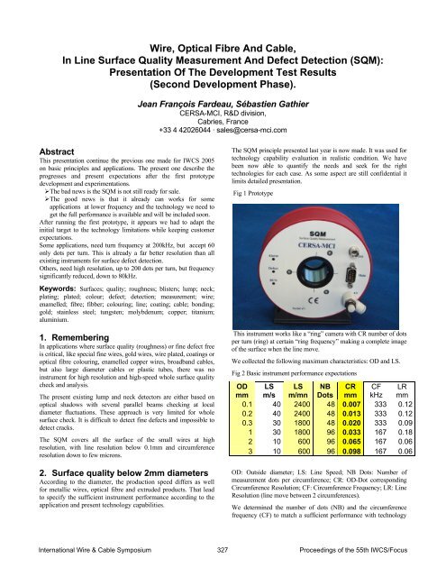
Fig 1 Prototype<br />
Keywords: <strong>Surface</strong>s; quality; roughness; blisters; lump; neck;<br />
plating; plated; colour; defect; detection; measurement; wire;<br />
enamelled; fibre; fibber; colouring; line; coating; cable; bonding;<br />
gold; stainless steel; tungsten; molybdenum; copper; titanium;<br />
aluminium.<br />
1. Remembering<br />
<strong>In</strong> applications where surface quality (roughness) or fine defect free<br />
is critical, like special fine wires, gold wires, wire plated, coatings or<br />
optical fibre colouring, enamelled copper wires, broadband cables,<br />
but also large diameter cables or plastic tubes, there was no<br />
instrument for high resolution and high-speed whole surface quality<br />
check and analysis.<br />
The present existing lump and neck detectors are either based on<br />
optical shadows with several parallel beams checking at local<br />
diameter fluctuations. These approach is very limited for whole<br />
surface check. It is difficult to detect fine defects and impossible to<br />
detect cracks.<br />
The SQM covers all the surface of the small wires at high<br />
resolution, with line resolution below 0.1mm and circumference<br />
resolution down to few microns.<br />
2. <strong>Surface</strong> quality below 2mm diameters<br />
According to the diameter, the production speed differs as well<br />
for metallic wires, optical fibre and extruded products. That lead<br />
to specify the sufficient instrument performance according to the<br />
application and present technology capabilities.<br />
This instrument works like a “ring” camera with CR number of dots<br />
per turn (ring) at certain “ring frequency” making a complete image<br />
of the surface when the line move.<br />
We collected the following maximum characteristics: OD and LS.<br />
Fig 2 Basic instrument performance expectations<br />
OD<br />
mm<br />
LS<br />
m/s<br />
LS<br />
m/mn<br />
NB<br />
Dots<br />
CR<br />
mm<br />
CF<br />
kHz<br />
LR<br />
mm<br />
0.1 40 2400 48 0.007 333 0.12<br />
0.2 40 2400 48 0.013 333 0.12<br />
0.3 30 1800 48 0.020 333 0.09<br />
1 30 1800 96 0.033 167 0.18<br />
2 <strong>10</strong> 600 96 0.065 167 0.06<br />
3 <strong>10</strong> 600 96 0.098 167 0.06<br />
OD: Outside diameter; LS: <strong>Line</strong> Speed; NB Dots: Number of<br />
measurement dots per circumference; CR: OD-Dot corresponding<br />
Circumference Resolution; CF: Circumference Frequency; LR: <strong>Line</strong><br />
Resolution (line move between 2 circumferences).<br />
We determined the number of dots (NB) and the circumference<br />
frequency (CF) to match a sufficient performance with technology<br />
<strong>In</strong>ternational <strong>Wire</strong> & <strong>Cable</strong> Symposium 327 Proceedings of the 55th IWCS/Focus
capabilities for each type of applications. This meet the customer<br />
demands and becomes our present target. It meets high resolution<br />
for very high speed lines with LR (pitch) below 0.15mm at<br />
2400m/mn. This is especially important for enamelled wires, optical<br />
fibres and fine extruded products.<br />
Nevertheless, other characteristics can be made, especially for<br />
surface quality of metallic wires where frequency is not critical but<br />
resolution might be much more important.<br />
We define a basic rule for instrument design: NB * CF = K with K<br />
about 16000. ex.: 48x333 or 96*167, etc…due to the present<br />
technology limitation. But the products terms could also be NB =<br />
200 and CF =80kHz.<br />
We also have to consider that there is limited interest to increase the<br />
number of dots for very fine wires. For 0.1mm and 48 dots, the dot<br />
pitch is 0.12 mm and dot size (CR) is 7µm. For NB=200 it would be<br />
1.5µm with 4 time less energy (smaller dot size). <strong>In</strong> that case surface<br />
quality should be excellent (gold, polymers, …) to keep continuous<br />
signal. For most of the cases, micronic surfaces are not perfect. That<br />
means it is better to integrate larger dot surface for better signal<br />
quality and defect sensitivity.<br />
Below 0.3mm OD, it covers fine wires, optical fibres and fine<br />
extruded products. From 0.3 to 3mm it is more in the common<br />
product sizes for wires, POF and extruded products.<br />
As the light energy reflected by the wire is proportional to the<br />
diameter, below 0.1mm it becomes very weak. That leads to seek<br />
higher light transfer efficiency, specific light sources, sensors, but<br />
mainly sensor amplification.<br />
Fig 3 instrument principle<br />
Photo-sensor A<br />
Ring of<br />
elementary<br />
light sources<br />
Zone 2<br />
Zone 1<br />
Measurement<br />
area<br />
With “i” = incident light energy density. 2*dθ is the sensor<br />
aperture, then constant and determine the dot size on the<br />
wire.<br />
Fig 4 Reflected light on the wire<br />
Fig 5. Light energy distribution<br />
E<br />
Sensor<br />
aperture<br />
120°<br />
r<br />
OD<br />
When the light source point rotates around the wire, the sensor<br />
received an energy varying in “cos” shape on ±.60° on the wire.<br />
For this instruments it is difficult to get significant results without<br />
the basic test structure, which is the electronic, optical banc and<br />
sensor systems. This is why we made it running first in order to be<br />
able to get the results in the right conditions.<br />
Fig 6 <strong>In</strong>strument design<br />
θ<br />
θ<br />
2*dθ<br />
dθ<br />
<strong>Wire</strong><br />
Zone 3<br />
Glass tube<br />
Photo-sensor B<br />
Photo-sensor<br />
Source/Photo-sensor<br />
locations<br />
Zone 1/ sensors A + C<br />
Zone 2/ sensors B + A<br />
Zone 3/ sensors C + B<br />
Scheme n° 1:<br />
Energy scattered by the wire in the θ direction for dθ:<br />
E = r*dθ*Cosθ*i<br />
Ring of light sources<br />
Sensor systems<br />
Fig 7 Realisation<br />
<strong>In</strong>ternational <strong>Wire</strong> & <strong>Cable</strong> Symposium 328 Proceedings of the 55th IWCS/Focus
This present design work today at lower frequencies for diameters<br />
above 0.5mm.<br />
Our next step, by October, November 2006 is to include a new light<br />
source to significantly increase light energy density and new sensor<br />
technology at high speed and much higher sensitivity to validate the<br />
capability to measure below 0.1mm.<br />
3. Typical in line applications<br />
3.1 <strong>Wire</strong> industry:<br />
• <strong>Surface</strong> quality (roughness), for gold, stainless steel,<br />
tungsten wires.<br />
• Plated wire to detect missing plating area.<br />
• Coated wires or fibres, to detect lump and neck or missing<br />
coating.<br />
• Enameled wires for blister detection<br />
3.2 <strong>Optical</strong> fibre industry:<br />
• Coating defect (lump and neck).<br />
• Coloring line, to detect defects, missing coloring layer.<br />
3.3 <strong>Cable</strong>s:<br />
• <strong>In</strong>sulated wires and small cables (broad band): lump and<br />
neck, local defects.<br />
4. Development plan and marketing<br />
The present works lead us to plan the last tests within now few<br />
months and the first industrial tests early 2007.<br />
The first sales are expected end of for first quarter 2007, one year<br />
later than our initial expectations.<br />
<strong>In</strong>ternational <strong>Wire</strong> & <strong>Cable</strong> Symposium 329 Proceedings of the 55th IWCS/Focus