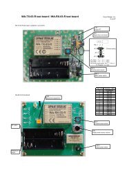
PDF:512KB - Circuit Design, Inc.
PDF:512KB - Circuit Design, Inc.
PDF:512KB - Circuit Design, Inc.

You also want an ePaper? Increase the reach of your titles
YUMPU automatically turns print PDFs into web optimized ePapers that Google loves.
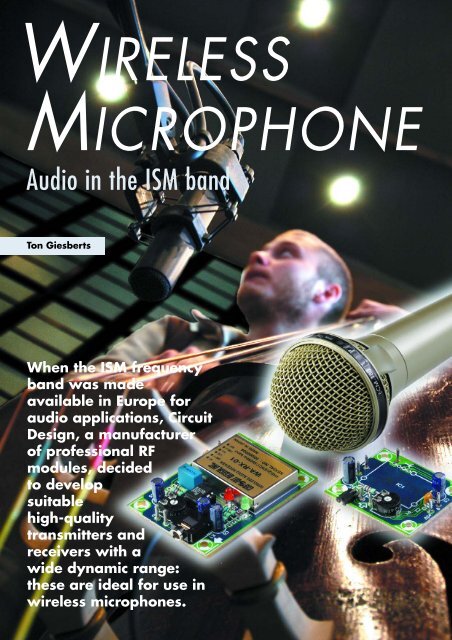
WIRELESS<br />
MICROPHONE<br />
Audio in the ISM band<br />
Ton Giesberts<br />
When the ISM frequency<br />
band was made<br />
available in Europe for<br />
audio applications, <strong>Circuit</strong><br />
<strong>Design</strong>, a manufacturer<br />
of professional RF<br />
modules, decided<br />
to develop<br />
suitable<br />
high-quality<br />
transmitters and<br />
receivers with a<br />
wide dynamic range:<br />
these are ideal for use in<br />
wireless microphones.
The WA-TX-01 (transmitter) and WA-<br />
RX-01 (receiver) modules represent a<br />
novel concept in the wireless transmission<br />
of audio signals. Thanks to low<br />
power consumption, the technology<br />
lends itself to a wide range of audio<br />
applications. The transmitter and the<br />
receiver include components such as<br />
SAW filters, SAW resonators and noise<br />
reduction ICs.<br />
These key components allow the<br />
development of small high-quality<br />
audio modules in accordance with<br />
European radio regulations and with<br />
EMC and R&TTE guidelines. This<br />
means that a wireless link can be<br />
added to an audio device without having<br />
to worry about a complicated,<br />
expensive and time-consuming certification<br />
process. The frequency channel<br />
used by each module is fixed, but there<br />
are four separate channels available in<br />
the band from 863 MHz to 865 MHz,<br />
and so multiple systems can coexist in<br />
the same location.<br />
Dynamic<br />
transmission<br />
The maximum sound<br />
pressure level (SPL) which<br />
can be tolerated by humans is<br />
140 dB SPL , which is measured relative<br />
to the minimum audible sound<br />
pressure level of 0 dB SPL = 20 µPa. In a<br />
quiet room the background noise level<br />
is about 20 dB SPL , and the sound pressure<br />
level of the human voice is around<br />
120 dB SPL . It can therefore be seen that<br />
the dynamic range required for a normal<br />
wireless audio transmission system<br />
is around 100 dB.<br />
If an audio frequency of 15 kHz is<br />
transmitted using analogue frequency<br />
modulation, the required bandwidth<br />
(BW) is given by:<br />
BW =<br />
2 (maximum frequency deviation +<br />
maximum modulation frequency) [Hz]<br />
Unfortunately any FM circuit must suffer<br />
from residual sideband noise originating<br />
in the PLL or crystal oscillator.<br />
As a rule of thumb, we can reckon with<br />
a residual noise, measured in terms of<br />
frequency shift, of around 50 Hz. For a<br />
dynamic range of 100 dB (i.e., a factor<br />
of 100 000), we therefore need an overall<br />
frequency deviation of 50 × 100 000<br />
= 5 MHz. As you might expect, this<br />
means that the required bandwidth is<br />
much greater than that available in<br />
this application. For comparison, FM<br />
radio transmissions make do with a<br />
0 dB<br />
-20 dB<br />
-40 dB<br />
-60 dB<br />
-80 dB<br />
-100 dB<br />
Transmitter<br />
input signal<br />
Compressor<br />
maximum deviation of 75 kHz in a<br />
bandwidth of 180 kHz (mono) or<br />
264 kHz (stereo plus traffic data).<br />
In order to solve this problem while<br />
keeping within the legal restrictions on<br />
frequency deviation, a compressor is<br />
built into the transmitter and an<br />
expander into the receiver. This technique<br />
is called a compander noise<br />
reduction system (Figure 1).<br />
The Dolby noise reduction system<br />
varies the compression ratio with frequency.<br />
The compander noise reduction<br />
system used here, on the other<br />
hand, fixes the compression ratio at 2:1<br />
over the entire frequency range, thus<br />
halving the dynamic range of the signal.<br />
In the expander, whose ratio is set<br />
to 1:2, the exact opposite occurs, and<br />
the dynamic range is doubled again. A<br />
dynamic range of 100 dB is thus<br />
reduced to 50 dB for transmission.<br />
We can now recalculate the frequency<br />
deviation required. With a residual<br />
noise of 50 Hz we need a frequency<br />
deviation of 500 Hz for a 20 dB<br />
dynamic range, 5 kHz for 40 dB, and<br />
20 kHz for 52 dB. A wireless system<br />
with a signal-to-noise ratio of 50 dB<br />
can carry sound signals with an original<br />
dynamic range of 100 dB.<br />
Why, in this ‘digital age’, do we<br />
employ analogue transmission techniques<br />
for the wireless microphone<br />
rather than, for example, PCM There<br />
are several reasons. Many countries<br />
have not allocated a dedicated frequency<br />
band for digital wireless<br />
microphones. Digital transmissions<br />
using PCM require a wide frequency<br />
band, which is not readily available<br />
Compander process<br />
Radio<br />
transmission<br />
∆ f limit level<br />
-10 dB<br />
-20 dB<br />
-30 dB<br />
-40 dB<br />
-50 dB<br />
-60 dB<br />
FM residual noise<br />
040402 - 13<br />
Figure 1. Use of a compander for noise reduction.<br />
Expander<br />
Receiver<br />
output signal<br />
FM residual noise<br />
below 1 GHz. Above 1 GHz ‘dead<br />
spots’ start to appear, meaning that<br />
these frequencies are not suitable for<br />
live use where the performer may<br />
move around between various positions<br />
on stage. Finally, conversion to<br />
digital requires much more power,<br />
making it less practical to run the<br />
device from small batteries.<br />
If desired, the modules (both receiver<br />
and transmitter) can be operated from<br />
a 1.5 V battery via a low-noise DC-DC<br />
converter available from <strong>Circuit</strong><br />
<strong>Design</strong>. In order to achieve the 100 dB<br />
dynamic range that is possible with<br />
the wireless microphone, the noise produced<br />
by the DC-DC converter muct<br />
be less than –60 dBm. The WA-DC-01<br />
DC-DC converter requires an input<br />
voltage of at least 0.9 V and can produce<br />
an output voltage of 3 V at the<br />
maximum load current of 50 mA.<br />
The transmitter<br />
0 dB<br />
-20 dB<br />
-40 dB<br />
-60 dB<br />
-80 dB<br />
-100 dB<br />
Figure 2 shows the functional blocks<br />
of the WA-TX-01 transmitter. We will<br />
look at each in turn.<br />
Input buffer (BUF)<br />
This circuit is an input buffer for the<br />
microphone capsule or other sound<br />
signal source. The maximum input<br />
level is –15 dBV and the input impedance<br />
is 7.5 kΩ. If the maximum output<br />
level of the signal source is not sufficient,<br />
a low-noise amplifier must be<br />
connected before the buffer. If the signal<br />
source level is too high, an attenuator<br />
should be used.<br />
2/2005 - elektor electronics 21
WA-TX-01<br />
AF LPF<br />
SAW Resonator<br />
RF LPF<br />
interference to adjacent channels is<br />
kept within the permitted limits.<br />
AUDIO<br />
SIGNAL<br />
INPUT<br />
PA<br />
Compressor<br />
Reference<br />
Power<br />
Supply<br />
Pre-<br />
Emphasis<br />
Compressor circuit<br />
Gain Cell<br />
Rectifier<br />
SUM<br />
AMP<br />
20kΩ<br />
20kΩ<br />
OSC. MOD<br />
PA<br />
2V7<br />
AVR<br />
040402 - 14<br />
ANT<br />
+3V<br />
GND<br />
Oscillator and modulator<br />
In order to operate directly in the<br />
800 MHz band, a crystal-based SAW<br />
(surface acoustic wave) filter resonator<br />
with good temperature stability is<br />
used as the oscillating element. Frequency<br />
modulation is achieved using<br />
a varicap diode that forms part of the<br />
oscillator circuit.<br />
RF power amplifier (PA)<br />
This circuit steps the RF output of the<br />
oscillator up to the transmit power of<br />
about 5 mW.<br />
Figure 2. Block diagram of the transmitter module...<br />
Compressor<br />
The audio signal from the buffer stage<br />
is compressed using a ratio of 2:1. The<br />
compressor consists of a reference<br />
generator, a full-wave rectifier and a<br />
summing amplifier. The reference generator<br />
provides a bias voltage and a<br />
constant current to the other parts of<br />
the circuit.<br />
The full-wave rectifier circuit rectifies<br />
the incoming signal with the aid of an<br />
external capacitor. The output current<br />
of the rectifier controls the gain cell<br />
amplifier. The time constant of the control<br />
loop is set, in part, using an external<br />
filter capacitor and an internal<br />
10 kΩ resistor. The summing amplifier<br />
adds the incoming signal and the signal<br />
from the gain cell amplifier together.<br />
The summing amplifier used in the<br />
compressor needs different properties<br />
from the one used in the expander, and<br />
so different components are used in<br />
the transmitter and in the receiver.<br />
Pre-emphasis<br />
To reduce noise at the upper end of the<br />
audio frequency range, which is a particular<br />
problem when using frequency<br />
modulation, this circuit boosts higher<br />
frequencies using a time constant of<br />
50 µs.<br />
AF low-pass filter (AF LPF)<br />
This circuit limits the bandwidth of the<br />
audio signal in order to ensure that<br />
RF low-pass filter (RF LPF)<br />
This circuit attenuates the second and<br />
higher harmonics of the transmitted<br />
signal and provides antenna impedance<br />
matching.<br />
Voltage regulator (AVR)<br />
This circuit provides a stable 2.7 V supply<br />
for the whole circuit. It operates<br />
from a battery supply of between 3 V<br />
and 9 V.<br />
The receiver<br />
The block diagram of the WA-RX-01<br />
receiver module shown in Figure 3 is<br />
practically the mirror image of the<br />
transmitter, using similar components.<br />
RF band-pass filter (SAW)<br />
The 800 MHz frequency band used in<br />
this wireless audio system is extracted<br />
using this filter. A high-selectivity SAW<br />
WA-RX-01<br />
ANT<br />
SAW<br />
LNA<br />
MIX<br />
10.7Mhz<br />
IF1<br />
IF2<br />
10.7Mhz<br />
IF3<br />
DET<br />
De-<br />
Emphasis<br />
AF<br />
SW<br />
Expander<br />
AF<br />
OUT<br />
Ceramic discriminator<br />
COM<br />
LED<br />
OSC<br />
RSSI<br />
crystal<br />
MUTE<br />
Reference<br />
Power<br />
Supply<br />
Expander circuit<br />
SUM<br />
AMP<br />
2V7<br />
AVR +3V<br />
GND<br />
20kΩ<br />
Gain Cell<br />
20kΩ<br />
Rectifier<br />
040402 - 15<br />
Figure 3. ... and of the receiver module.<br />
22<br />
elektor electronics - 2/2005
filter is used to ensure that frequencies<br />
outside the band are eliminated.<br />
Oscillator (OSC)<br />
A quartz crystal oscillator is used to<br />
mix the incoming signal down to an<br />
intermediate frequency of 10.7 MHz.<br />
RF amplifier (LNA)<br />
A low-noise amplifier is used to<br />
amplify the 800 MHz frequency band<br />
by 10 dB.<br />
Mixer (MIX)<br />
This circuit creates an intermediate frequency<br />
of 10.7 MHz, produced by mixing<br />
the amplified received signal in the<br />
800 MHz band with the output of the<br />
oscillator.<br />
IF amplifier (IF1 to IF3)<br />
These provide a total gain of 100 dB,<br />
the final stage acting as a limiter.<br />
Before and after the amplifier chain,<br />
10.7 MHz ceramic filters are fitted to<br />
provide selectivity.<br />
FM detector (DET)<br />
This circuit demodulates the frequency-modulated<br />
IF signal.<br />
RSSI detector (RSSI)<br />
Signals from the middle of the IF<br />
amplifier chain are rectified producing<br />
a DC voltage proportional to the signal<br />
strength.<br />
Muting comparator (COM)<br />
The RSSI signal is compared to a preset<br />
voltage which can be adjusted<br />
using a potentiometer. If the level at<br />
the antenna input falls to 17 dBµV or<br />
less, the output signal is turned off.<br />
De-emphasis<br />
This compensates for the 50 µs preemphasis,<br />
making the overall frequency<br />
response of the system flat.<br />
AF amplifier (AF)<br />
This circuit amplifies the demodulated<br />
audio signal before it is passed to the<br />
expander.<br />
Analogue switch (SW)<br />
If the signal strength falls too far, the<br />
audio signal is muted using this<br />
switch. An LED indicates when this<br />
muting occurs.<br />
Expander<br />
The dynamic range of the audio signal<br />
is doubled by this circuit, which operates<br />
in much the same way as the<br />
compressor.<br />
AF output amplifier (AF)<br />
The output of the expander circuit is<br />
amplified again for output.<br />
Voltage regulator (AVR)<br />
This circuit provides the entire circuit<br />
with a stable 2.7 V supply from a battery<br />
voltage of between 3 V and 12 V.<br />
Interface<br />
Thanks to these complex modules that<br />
include almost all the necessary electronics,<br />
what remains is straightforward.<br />
Figure 4 shows the two parts of<br />
the circuit. In the transmitter we can<br />
either connect a microphone or any<br />
other desired audio source with a maximum<br />
output level of –15 dBV. In most<br />
cases, however, an electret microphone<br />
will be used. There is a small<br />
offset voltage present at the AF input<br />
with P1 adjusted to maximum: in our<br />
prototype we measured about 0.15 V. If<br />
a dynamic microphone is to be connected,<br />
it is essential to add a coupling<br />
capacitor. Alternatively, omit R1 and<br />
connect the dynamic microphone in<br />
place of the electret microphone. P1<br />
can be used to attenuate microphone<br />
signals that are too high, so that the<br />
radio module is not overdriven.<br />
The receiver circuit is slightly less simple.<br />
The receiver module has two outputs,<br />
one for the signal itself and one<br />
which indicates whether the signal<br />
strength is adequate or whether the<br />
muting circuit has been triggered.<br />
Since we have plenty of power to spare<br />
at the receiver (battery operation here<br />
is not essential) we can afford an extra<br />
indicator in the form of LED D1.<br />
In order to amplify the output of the<br />
receiver module (which, at 10 kΩ, is not<br />
exactly low impedance), we have<br />
added a buffer amplifier. This is a classical<br />
non-inverting AC amplifier built<br />
around a rail-to-rail opamp which can<br />
operate from a voltage of between 2.7 V<br />
and 12 V, almost the same range as for<br />
the module. We have shown a supply<br />
voltage of 5 V, although 3 V or 12 V<br />
would do just as well. If a different (nonrail-to-rail)<br />
opamp were used, a supply<br />
voltage of 5 V would be required. Many<br />
opamps will only operate correctly with<br />
a symmetric power supply of ±5 V or<br />
ANT1<br />
IC2<br />
WA-RX-01A<br />
AF<br />
IC1<br />
WA-TX-01<br />
ANT1<br />
ANT<br />
6<br />
GND2<br />
5<br />
VCC<br />
LED<br />
GND1<br />
AF<br />
4 3 2 1<br />
I<br />
V<br />
G<br />
A<br />
MIC1<br />
+3V<br />
2k2<br />
R1<br />
C1<br />
4µ7<br />
63V<br />
JP1<br />
P1<br />
10k<br />
C3<br />
10µ<br />
63V<br />
4 3 2 1<br />
C2<br />
100n<br />
040402 - 11<br />
+3V<br />
+3V<br />
BT1<br />
3V<br />
+5V<br />
+5V<br />
C8<br />
10µ<br />
63V<br />
C4<br />
R8<br />
470n<br />
560 Ω<br />
C7<br />
100n D2<br />
POWER<br />
R2<br />
D1<br />
560 Ω<br />
SIGNAL<br />
R3<br />
P2<br />
10k<br />
3 7<br />
IC3<br />
2<br />
220k<br />
220k<br />
R4<br />
R5 4<br />
TS921IN<br />
4k7<br />
C5<br />
6<br />
R6<br />
47Ω<br />
C6<br />
4µ7<br />
63V<br />
100k<br />
R7<br />
K1<br />
AF<br />
10µ 63V<br />
040402 - 12<br />
Figure 4. Interfaces for the radio modules.<br />
2/2005 - elektor electronics 23
C3<br />
IC1<br />
T<br />
0<br />
MIC1<br />
+3V<br />
C2<br />
P1<br />
R1<br />
AF<br />
T<br />
C1<br />
JP1<br />
040402-1<br />
IC2<br />
040402-1<br />
Figure 5. Two circuit boards make one radio link.<br />
COMPONENTS<br />
LIST<br />
Resistors:<br />
R1 = 2kΩ2<br />
R2,R8 = 560Ω*<br />
R3,R4 = 220kΩ<br />
R5 = 4kΩ7<br />
R6 = 47Ω<br />
R7 = 100kΩ<br />
P1,P2 = 10 kΩ preset<br />
Capacitors:<br />
C1,C6 = 4µF7 63V radial<br />
C2,C7 = 100nF<br />
C3,C5,C8 = 10µF 63V radial<br />
C4 = 470nF<br />
C7<br />
040402-1<br />
D2<br />
D1<br />
R2<br />
R8<br />
R6<br />
R7<br />
C4<br />
IC3<br />
C6<br />
R3<br />
R5<br />
R4<br />
C8<br />
P2<br />
K1<br />
C5<br />
+5V<br />
Semiconductors:<br />
D1 = LED, 3mm, green, low current<br />
D2 = LED, 3mm, red, low current<br />
IC1 = WA-TX-01 (<strong>Circuit</strong> <strong>Design</strong>)<br />
IC2 = WA-RX-01A (<strong>Circuit</strong> <strong>Design</strong>)<br />
IC3 = TS921IN (or equivalent rail-to-railopamp)<br />
Miscellaneous:<br />
JP1 = 2-way pinheader with jumper<br />
(angled if necessary)<br />
K1 = 3.5-mm jack socket, PCB mount<br />
(e.g. Conrad Electronics # 732893)<br />
BT1 = battery holder for two 1.5V<br />
batteries<br />
MIC1 = electret microphone<br />
PCB, no. 040402-1, available from The<br />
PCBShop<br />
0<br />
with an asymmetric 10 V supply. A further<br />
advantage of the TS921 used here<br />
is its high output drive capability: it can<br />
directly drive headphones or even two<br />
32 Ω headphone transducers wired in<br />
parallel, although in this case C6 should<br />
be replaced by a 100 µF 10 V type. The<br />
47 Ω output resistor protects the opamp<br />
from the inductive load of a shielded<br />
cable and from short circuits. Trimmer<br />
potentiometer P2 allows the gain to be<br />
adjusted from unity (P2 at minimum<br />
resistance) to 10 dB (P2 at maximum<br />
resistance). C6 removes any DC component<br />
from the output and R7 ensures<br />
that there is always a load at the output.<br />
Since the opamp has asymmetrical<br />
supplies, a capacitor (C5) is also<br />
required in the feedback circuit. R3 and<br />
R4 set the operating point of the opamp<br />
at half the supply voltage. C7 and C8<br />
provide extra power supply decoupling.<br />
At higher supply voltages it is necessary<br />
to increase the current-limiting<br />
resistors for the low-current LEDs so<br />
that the current through them does not<br />
exceed about 2 mA.<br />
We have designed a two-part printed<br />
circuit board to accommodate the radio<br />
modules and the few external components<br />
(Figure 5). The layout is designed<br />
for optimum audio performance.<br />
The components should be fitted to the<br />
board, observing that the transmitter<br />
module can only be fitted to the copper<br />
side. An ordinary 3.5 mm jack socket<br />
provides the audio output.<br />
All that remains are the antennas. In<br />
principle a stiff piece of wire with<br />
length 1/4 λ (78 mm at 860 MHz) will<br />
do the job; more professional antennas<br />
can be found on the <strong>Circuit</strong> <strong>Design</strong><br />
website at http://www.cdt21.com/.<br />
(040402-1)<br />
24<br />
elektor electronics - 2/2005
Frequency<br />
863.125 MHz; 863.625 MHz; 864.500 MHz; 864.875 MHz<br />
RF channels<br />
one (fixed)<br />
Emission code<br />
F3E<br />
Range<br />
approx. 50 m line-of-sight<br />
Signal-to-noise ratio<br />
90 dB (with IHF-A filter)<br />
Audio frequency range<br />
50 Hz to 15 kHz ± 3.5 dB (output level –50 dBV ± 3 dB)<br />
THD<br />
2 % (@ AF 1 kHz, deviation = 15 kHz or 7.5 kHz)<br />
Pre-emphasis 50 µs<br />
Operating temperature 0 °C to 50 °C<br />
Transmitter<br />
Oscillator<br />
SAW oscillator, crystal-based<br />
RF power<br />
2 mW<br />
Frequency stability<br />
±10 kHz<br />
Pre-emphasis 50 µs<br />
Noise reduction<br />
Compressor<br />
Spurious emission<br />
1 µW maximum<br />
Deviation<br />
15 kHz (1 kHz @ –25 dBV)<br />
Audio input level<br />
–115 dBV to –15 dBV (1 kHz)<br />
Audio input impedance<br />
5 kΩ<br />
Supply voltage<br />
3 V to 9 V<br />
Maximum module current consumption<br />
25 mA<br />
Measured current consumption 17 mA @ 3 V<br />
Receiver<br />
Receiver type<br />
Superheterodyne<br />
Mixer oscillator<br />
Crystal-controlled<br />
Intermediate frequency<br />
10.7 MHz<br />
Noise reduction<br />
Expander<br />
Sensitivity 21 dBµV (@ THD 2 %)<br />
Squelch sensitivity<br />
17 dBµV ±4 dB<br />
Audio output level (at module) –20 dBV (deviation = 15 kHz)<br />
Maximum –10 dBV<br />
(deviation = 30 kHz)<br />
Audio output impedance (at module) 10 kΩ<br />
Supply voltage<br />
3 V to 12 V<br />
Maximum module current consumption<br />
30 mA<br />
Measured current consumption (D2 on, R2 = R3 = 560 Ω)<br />
32 mA @ 3 V<br />
40 mA @ 5 V<br />
52 mA @ 9 V<br />
Note: 0 dBV = 0.775 V<br />
A<br />
B<br />
d<br />
B<br />
r<br />
+4<br />
+2<br />
+0<br />
-2<br />
-4<br />
-6<br />
-8<br />
-10<br />
A<br />
-12<br />
-14<br />
-16<br />
-18<br />
-20<br />
-22<br />
-24<br />
-26<br />
20 50 100 200 500 1k 2k 5k 10 k 20 k<br />
Hz 040402 - 16<br />
10<br />
8<br />
6<br />
5<br />
4<br />
3<br />
%<br />
2<br />
Curve A shows the overall transfer characteristic of the entire<br />
radio link, measured at minimum gain (green) and maximum<br />
gain (red). The input signal to the transmitter was at –46 dBV<br />
(approximately 5 mV). The output signal at maximum gain was<br />
at –31 dBV. The output signal of the receiver is 5 dB above the<br />
input level to the transmitter. With a higher input signal level the<br />
response falls off somewhat at higher frequencies, but the amplitude<br />
at 5.5 kHz is up to 3 dB higher than that at 1 kHz.<br />
Curve B shows the distortion (plus noise) at the output of the<br />
receiver against signal level, measured over the frequency<br />
range from 22 Hz to 22 kHz. The optimum value appears to<br />
occur with an input signal level at the transmitter of 5 mV. In this<br />
case the input signal is raised from –70 dBV to –15 dBV with<br />
the gain at the receiver is at a maximum. This is more than adequate<br />
for speech signals.<br />
Curve C shows the frequency spectrum with an input signal<br />
level at the transmitter of 5 mV. Most of the distortion is at the<br />
second harmonic. In this case the THD+N figure is 0.85 %<br />
(over the frequency range from 22 Hz to 22 kHz).<br />
C<br />
d<br />
B<br />
r<br />
A<br />
1<br />
0.8<br />
0.6<br />
-60 -50 -40 -30 -20 -10 +0 +10<br />
dBV 040402 - 17<br />
+0<br />
-10<br />
-20<br />
-30<br />
-40<br />
-50<br />
-60<br />
-70<br />
-80<br />
-90<br />
-100<br />
20 50 100 200 500 1k 2k 5k 10 k 20 k<br />
Hz<br />
040402 - 18<br />
2/2005 - elektor electronics 25
040402-1<br />
non reflected<br />
040402-1<br />
reflected