STD-302N-R 429MHz Operation Guide - Circuit Design, Inc.
STD-302N-R 429MHz Operation Guide - Circuit Design, Inc.
STD-302N-R 429MHz Operation Guide - Circuit Design, Inc.

Create successful ePaper yourself
Turn your PDF publications into a flip-book with our unique Google optimized e-Paper software.
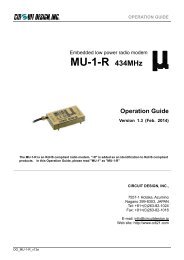
OPERATION GUIDE<br />
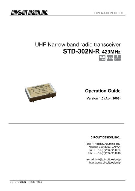
UHF Narrow band radio transceiver<br />
<strong>STD</strong>-<strong>302N</strong>-R <strong>429MHz</strong><br />
<strong>Operation</strong> <strong>Guide</strong><br />
Version 1.0 (Apr. 2008)<br />
CIRCUIT DESIGN, INC.,<br />
7557-1 Hotaka, Azumino-city,<br />
Nagano 399-8303 JAPAN<br />
Tel: + +81-(0)263-82-1024<br />
Fax: + +81-(0)263-82-1016<br />
e-mail: info@circuitdesign.jp<br />
http://www.circuitdesign.jp<br />
OG_<strong>STD</strong>-<strong>302N</strong>-R-429M_v10e
OPERATION GUIDE<br />
CONTENTS<br />
GENERAL DESCRIPTION & FEATURES ...........................3<br />
SPECIFICATIONS <strong>STD</strong>-<strong>302N</strong>-R 429 MHz .......................4<br />
PIN DESCRIPTION .............................................................5<br />
FREQUENCY TABLE ..........................................................7<br />
BLOCK DIAGRAM...............................................................8<br />
DIMENSIONS......................................................................9<br />
PLL IC CONTROL .............................................................10<br />
PLL IC control ..................................................................10<br />
How to calculate the setting values for the PLL register ........ 11<br />
Method of serial data input to the PLL.................................12<br />
TIMING CHART.................................................................13<br />
PLL FREQUENCY SETTING REFERENCE .....................15<br />
CAUTIONS & WARNINGS ................................................16<br />
OG_<strong>STD</strong>-<strong>302N</strong>-R-429M_v10e<br />
2<br />
<strong>Circuit</strong> <strong>Design</strong>, <strong>Inc</strong>.
OPERATION GUIDE<br />
GENERAL DESCRIPTION & FEATURES<br />
General Description<br />
The UHF FM narrow band semi-duplex radio data module <strong>STD</strong>-<strong>302N</strong>-R is an <strong>STD</strong>-T67 compliant,<br />
high performance transceiver designed for use in industrial applications requiring long range, high<br />
performance and reliability.<br />
All high frequency circuits are enclosed inside a robust housing to provide superior resistance<br />
against shock and vibration. A narrow band technique enables high interference rejection and<br />
concurrent operation with multiple modules.<br />
<strong>STD</strong>-<strong>302N</strong>-R <strong>429MHz</strong>, a narrowband module with 12.5 kHz channel steps, achieves high TX/RX<br />
switching speed, making it an ideal RF unit for inclusion in feedback systems.<br />
This product is designed to meet the basic specifications of the standard, however it has not been<br />
certified for conformity with the technical regulations. Users are required to perform the<br />
procedures for certification with their final products after installing this product in their systems.<br />
Features<br />
‣ 10 mW RF power, 3.0 V operation<br />
‣ Programmable RF channel<br />
‣ Fast TX/RX switching time<br />
‣ High sensitivity -120 dBm<br />
‣ Excellent mechanical durability, high vibration & shock resistance<br />
‣ <strong>STD</strong>-T67 compliance<br />
‣ EU RoHS compliance<br />
Applications<br />
‣ Telemetry<br />
Water level monitor for rivers, dams, etc.<br />
Monitoring systems for environmental data such as temperature, humidity, etc.<br />
Transmission of measurement data (pressure, revolution, current, etc) to PC<br />
Security alarm monitoring<br />
‣ Telecontrol<br />
Industrial remote control systems<br />
Remote control systems for factory automation machines<br />
Control of various driving motors<br />
‣ Data transmission<br />
RS232/RS485 serial data transmission<br />
OG_<strong>STD</strong>-<strong>302N</strong>-R-429M_v10e<br />
3<br />
<strong>Circuit</strong> <strong>Design</strong>, <strong>Inc</strong>.
SPECIFICATIONS<br />
<strong>STD</strong>-<strong>302N</strong>-R 429 MHz<br />
OPERATION GUIDE<br />
* The MIN/TYP/MAX values for the RF output power and BER are specified in the range of operation environment temperature.<br />
* All values in the Specification column are specified at 25 ºC+/-10 ºC unless otherwise noted.<br />
General characteristics<br />
Item Units MIN TYP MAX Remarks<br />
Communication method<br />
One way, Half-duplex<br />
Emission class<br />
F1D<br />
Operating frequency range MHz 429.25 429.7375<br />
<strong>Operation</strong> temperature range °C -20 60 No dew condensation<br />
Storage temperature range °C -30 75 No dew condensation<br />
Aging rate ( / year) ppm -1 1 TX freq., RX Lo freq.<br />
Initial frequency tolerance * ppm -1.5 1.5 TX freq., RX Lo freq. At delivery<br />
Dimensions mm 30 x 50 x 9 mm Not including protrusion<br />
Weight g 25 g<br />
* Initial frequency tolerance: At delivery<br />
Initial frequency tolerance is defined as frequency drift at delivery within 1 year after the final adjustment<br />
Electrical specification <br />
Item MIN TYP MAX Remarks<br />
Oscillation type<br />
PLL controlled VCO<br />
Frequency stability (-20 to 60°C) ppm -4 4 Reference frequency at 25 °C<br />
TX/RX switching time ms 15 20 DI/DO<br />
Channel step kHz 12.5<br />
Data rate bps 2400 4800 DO/DI<br />
Max. pulse width ms 15 20 DO/DI<br />
Min. pulse width us 200 DO/DI<br />
Data polarity Positive DI vs DO<br />
PLL reference frequency MHz 21.25 TCXO<br />
PLL response ms 30 60 from PLL setting to LD out<br />
Antenna impedance Ω 50 Nominal<br />
Operating voltage V 3.0 5.5<br />
TX consumption current mA 44 48 Vcc = 3.0 V<br />
RX consumption current mA 26 30 Vcc = 3.0 V<br />
For PLL interface, refer to the documents of MB15E03SLP and use it within the specification.<br />
Transmitter part<br />
Item MIN TYP MAX Remarks<br />
RF output power mW 5 9 12 Conducted 50 Ω 429.5 MHz<br />
Deviation kHz +/- 1.7 +/- 2.0 +/- 2.3 PN9 4800 bps<br />
DI input level V 0 5.5 L= GND, H = 3 V- Vcc<br />
Residual FM noise kHz 0.17 DI=L, LPF=20 kHz<br />
Spurious emission dBm - 37 - 27 Conducted 50Ω<br />
Adjacent CH power dB 40 PN9 4800 bps<br />
Occupied freq. bandwidth kHz 8.5 PN9 4800 bps<br />
OG_<strong>STD</strong>-<strong>302N</strong>-R-429M_v10e<br />
4<br />
<strong>Circuit</strong> <strong>Design</strong>, <strong>Inc</strong>.
OPERATION GUIDE<br />
Receiver part<br />
Item MIN TYP MAX Remarks<br />
Receiver type<br />
Double superheterodyne<br />
1st IF frequency MHz 21.7<br />
2nd IF frequency kHz 450<br />
Maximum input level dBm 10<br />
BER (0 error/2556 bits) *1 dBm -108 -115 PN 9 4800bps<br />
BER (1 % error) *2 dBm -120 PN 9 4800bps<br />
Sensitivity 12dB/ SINAD dBm -120 fm1 k/ dev 2 kHz CCITT<br />
Spurious response rejections *3 dB<br />
70 1 st Mix, 2 signal method, 1 % error<br />
55 2 nd Mix, 2 signal method, 1 % error<br />
Adjacent CH selectivity *3 dB 50<br />
+/- 12.5 kHz,<br />
2 signal method, 1 % error<br />
Blocking dB 84<br />
Jamming signal +/- 1MHz<br />
2 signal method, 1% error<br />
Intermodulation *4 dB 50 2 signal method, 1 % error<br />
DO output level V 0 2.8 L = GND H = 2.8 V<br />
RSSI rising time<br />
ms<br />
30 50 CH shift of 25 kHz (from PLL setup)<br />
50 70 When power ON (from PLL setup)<br />
50 100 CH shift of 25 kHz (from PLL setup)<br />
Time until valid Data-out *5 ms<br />
70 120 When power ON (from PLL setup)<br />
Spurious radiation (1 st Lo) dBm -60 -54 Conducted 50 Ω<br />
RSSI<br />
mV<br />
300 350 400 With -97 dBm at 429.5 MHz<br />
190 240 290 With -113 dBm at 429.5 MHz<br />
Specifications are subject to change without prior notice<br />
Notice<br />
• Communication range depends on the operation environment and ambient surrounding<br />
• The time required until a stable DO is established may get longer due to the possible frequency drift caused<br />
by operation environment changes, especially when switching from TX to RX, from RX to TX and changing<br />
channels. Please make sure to optimize the timing. The recommended preamble is more than 20 ms.<br />
• Antenna connection is designed as pin connection.<br />
• RF output power, sensitivity, spurious emission and spurious radiation levels may vary with the pattern used<br />
between the RF pin and the coaxial connection. Please make sure to verify those parameters before use.<br />
• The feet of the shield case should be soldered to the wide GND pattern to avoid any change in characteristics.<br />
Notes about the specification values<br />
*1 BER: RF level where no error per 2556 bits is confirmed with the signal of PN9 and 4800 bps.<br />
*2 BER (1 % error): RF level where 1% error per 2556 bits is confirmed with the signal of PN9 and 4800 bps.<br />
*3 Spurious response, CH selectivity: Jamming signal used in the measurement is unmodulated.<br />
*4 Intermodulation: Ratio between the receiver input level with BER 1% and the signal level (PN9 4800 bps)<br />
added at the points of 'Receiving frequency - 200 kHz ' + ' Receiving frequency -100kHz' with which BER 1%<br />
is achieved.<br />
*5 Time until valid Data-out: Valid DO is determined at the point where Bit Error Rate meter starts detecting the<br />
signal of 4800bps, 1010 repeated signal.<br />
Conditions:<br />
All specifications are specified based on the data measured in a shield room using the PLL setting controller<br />
board prepared by <strong>Circuit</strong> <strong>Design</strong>.<br />
Measuring equipment:<br />
SG=ANRITSU communication analyzer MT2605<br />
Spectrum analyzer = ANRITSU MS2663G, BER measure = ANRITSU MP1201G<br />
OG_<strong>STD</strong>-<strong>302N</strong>-R-429M_v10e<br />
5<br />
<strong>Circuit</strong> <strong>Design</strong>, <strong>Inc</strong>.
OPERATION GUIDE<br />
PIN DESCRIPTION<br />
Pin name I/O Description Equivalent circuit<br />
RF<br />
I/O<br />
RF input terminal<br />
Antenna impedance nominal 50 Ω<br />
SAW FILTER<br />
47P<br />
100nH<br />
RF<br />
GND<br />
GND<br />
I<br />
GROUND terminal<br />
The GND pins and the feet of the shield case<br />
shoud be connected to the wide GND<br />
pattern.<br />
VCC<br />
I<br />
Power supply terminal<br />
DC 3.0 to 5.5 V<br />
2.8V<br />
22µ 47P<br />
REG<br />
10µ<br />
VCC<br />
47P<br />
TXSEL<br />
I<br />
TX select terminal<br />
GND = TXSEL active<br />
To enable the transmitter circuits, connect<br />
TXSEL to GND and RXSEL to OPEN or 2.8<br />
V.<br />
2.8V<br />
10<br />
2.8V 20K<br />
TXSEL<br />
RXSEL<br />
I<br />
RX select terminal<br />
GND= RXSEL active<br />
To enable the receiver circuits, connect<br />
RXSEL to GND and TXSEL to OPEN or 2.8<br />
V.<br />
2.8V<br />
10<br />
2.8V 20K<br />
RXSEL<br />
AF<br />
I<br />
Analogue output terminal<br />
There is DC offset of approx. 1 V.<br />
Refer to the specification table for amplitude<br />
level.<br />
CLK<br />
I<br />
PLL data setting input terminal<br />
Interface voltage H = 2.8 V, L = 0 V<br />
MB15E03<br />
2K<br />
CLK<br />
DATA<br />
I<br />
PLL data setting input terminal<br />
Interface voltage H = 2.8 V, L = 0 V<br />
MB15E03<br />
2K<br />
DATA<br />
LE<br />
I<br />
PLL data setting input terminal<br />
Interface voltage H = 2.8 V, L = 0 V<br />
MB15E03<br />
2K<br />
LE<br />
OG_<strong>STD</strong>-<strong>302N</strong>-R-429M_v10e<br />
6<br />
<strong>Circuit</strong> <strong>Design</strong>, <strong>Inc</strong>.
OPERATION GUIDE<br />
2.8V<br />
LD<br />
O<br />
PLL lock/unlock monitor terminal<br />
Lock = H (2.8 V), Unlock = L (0 V)<br />
MB15E03<br />
102<br />
2K<br />
LD<br />
RSSI<br />
O<br />
Received Signal Strength Indicator terminal<br />
2.8V<br />
DO<br />
O<br />
Data output terminal<br />
Interface voltage: H=2.8V, L=0V<br />
10K<br />
102<br />
2K<br />
DO<br />
DI<br />
I<br />
Data input terminal<br />
Interface voltage: H=2.8 to Vcc, L=0V<br />
Input data pulse width Min.208 µs Max.5 ms<br />
OG_<strong>STD</strong>-<strong>302N</strong>-R-429M_v10e<br />
7<br />
<strong>Circuit</strong> <strong>Design</strong>, <strong>Inc</strong>.
OPERATION GUIDE<br />
Frequency table (<strong>STD</strong>-T67)<br />
Channel number Operating frequency (MHz) Transmission time restriction<br />
1 429.1750<br />
2 429.1875<br />
3 429.2000<br />
Transmission for 40 sec, pause for 2 sec<br />
4 429.2125<br />
5 429.2250<br />
6 429.2375<br />
7 429.2500<br />
8 429.2625<br />
9 429.2750<br />
10 429.2875<br />
11 429.3000<br />
12 429.3125<br />
13 429.3250<br />
14 429.3750<br />
15 429.3875<br />
16 429.3625<br />
17 429.3750<br />
18 429.3875<br />
19 429.4000<br />
20 429.4125<br />
21 429.4250<br />
22 429.4375<br />
23 429.4500<br />
24 429.4625<br />
25 429.4750<br />
26 429.4875<br />
27 429.5000<br />
28 429.5125<br />
29 429.5250<br />
30 429.5375<br />
31 429.5500<br />
32 429.5625<br />
33 429.5750<br />
34 429.5875<br />
35 429.6000<br />
36 429.6125<br />
37 429.6250<br />
38 429.6375<br />
39 429.6500<br />
40 429.6625<br />
41 429.6750<br />
42 429.6875<br />
43 429.7000<br />
44 429.7125<br />
45 429.7250<br />
46 429.7375<br />
Continuous transmission<br />
(Intermittent communication possible)<br />
OG_<strong>STD</strong>-<strong>302N</strong>-R-429M_v10e<br />
8<br />
<strong>Circuit</strong> <strong>Design</strong>, <strong>Inc</strong>.
OPERATION GUIDE<br />
BLOCK DIAGRAM <br />
OG_<strong>STD</strong>-<strong>302N</strong>-R-429M_v10e 9<br />
<strong>Circuit</strong> <strong>Design</strong>, <strong>Inc</strong>.
OPERATION GUIDE<br />
DIMENSIONS<br />
OG_<strong>STD</strong>-<strong>302N</strong>-R-429M_v10e 10<br />
<strong>Circuit</strong> <strong>Design</strong>, <strong>Inc</strong>.
OPERATION GUIDE<br />
PLL IC CONTROL<br />
• PLL IC control<br />
up to 1200MHz<br />
Figure 1<br />
VCO<br />
Voltage Controled<br />
Oscillator<br />
Fin<br />
Xf in<br />
CLK<br />
Data<br />
2kohm<br />
2kohm<br />
CLK<br />
DATA<br />
GND<br />
LE<br />
2kohm<br />
LE<br />
LPF<br />
+2.8v<br />
Do<br />
VCC<br />
PLL<br />
MB15E03SL<br />
PS<br />
ZC<br />
Vp<br />
LD/f out<br />
2kohm<br />
LD<br />
Reference Oscillator<br />
21.25MHz<br />
OSCout<br />
OSCin<br />
P<br />
R<br />
<strong>STD</strong>-302<br />
Control pin name<br />
#:Control v oltage = +2.8v<br />
<strong>STD</strong>-<strong>302N</strong>-R is equipped with an internal PLL frequency synthesizer as shown in Figure 1. The operation of<br />
the PLL circuit enables the VCO to oscillate at a stable frequency. Transmission frequency is set externally by<br />
the controlling IC. <strong>STD</strong>-<strong>302N</strong>-R has control terminals (CLK, LE, DATA) for the PLL IC and the setting data is<br />
sent to the internal register serially via the data line. Also <strong>STD</strong>-<strong>302N</strong>-R has a Lock Detect (LD) terminal that<br />
shows the lock status of the frequency. These signal lines are connected directly to the PLL IC through a 2 kΩ<br />
resistor.<br />
The interface voltage of <strong>STD</strong>-<strong>302N</strong>-R is 2.8 V, so the control voltage must be the same.<br />
<strong>STD</strong>-<strong>302N</strong>-R comes equipped with a Fujitsu MB15E03SL PLL IC. Please refer to the manual of the PLL IC.<br />
The following is a supplementary description related to operation with <strong>STD</strong>-<strong>302N</strong>-R. In this description, the<br />
same names and terminology as in the PLL IC manual are used, so please read the manual beforehand.<br />
OG_<strong>STD</strong>-<strong>302N</strong>-R-429M_v10e<br />
11<br />
<strong>Circuit</strong> <strong>Design</strong>, <strong>Inc</strong>.
OPERATION GUIDE<br />
• How to calculate the setting values for the PLL register<br />
The PLL IC manual shows that the PLL frequency setting value is obtained with the following equation.<br />
f vco = [(M x N)+A] x f osc / R -- Equation 1<br />
f vco : Output frequency of external VCO<br />
M: Preset divide ratio of the prescaler (64 or 128)<br />
N: Preset divide ratio of binary 11-bit programmable counter (3 to 2,047)<br />
A: Preset divide ratio of binary 7-bit swallow counter (0 ≤ A ≤ 127 A
OPERATION GUIDE<br />
• Method of serial data input to the PLL<br />
After the RF channel table plan is decided, the data needs to be allocated to the ROM table and read from<br />
there or calculated with the software.<br />
Together with this setting data, operation bits that decide operation of the PLL must be sent to the PLL.<br />
The operation bits for setting the PLL are as follows. These values are placed at the head of the reference<br />
counter value and are sent to the PLL.<br />
1. CS: Charge pump current select bit<br />
CS = 0 +/-1.5 mA select VCO is optimized to +/-1.5 mA<br />
2. LDS: LD/fout output setting bit<br />
LDS = 0 LD select Hardware is set to LD output<br />
3. FC: Phase control bit for the phase comparator<br />
FC = 1<br />
Hardware operates at this phase<br />
Figure 2<br />
1st Data<br />
2nd Data<br />
2nd data N11 N10 N9 N8 N7 N6 A1 CNT=0<br />
1st data<br />
CS<br />
LDS FC SW R14 R13 R1 CNT=1<br />
DATA<br />
MSB<br />
LSB<br />
Invalid Data<br />
CLK<br />
t1<br />
t2<br />
t3<br />
t6<br />
LE<br />
t0<br />
<strong>STD</strong>-302<br />
terminal name<br />
#: t0,t5 >= 100 ns t1,t2,t6 >= 20 ns t3,t4 >= 30 ns<br />
t4<br />
#: Keep the LE terminal at a low level, w hen w rite the data to the shift resister.<br />
t5<br />
The PLL IC, which operates as shown in the block diagram in the manual, shifts the data to the 19-bit shift<br />
register and then transfers it to the respective latch (counter, register) by judging the CNT control bit value<br />
input at the end.<br />
1. CLK [Clock]: Data is shifted into the shift register on the rising edge of this clock.<br />
2. LE [Load Enable]: Data in the 19-bit shift register is transferred to respective latches on the rising edge of<br />
the clock. The data is transferred to a latch according to the control bit CNT value.<br />
3. Data [Serial Data]: You can perform either reference counter setup or programmable counter setup first.<br />
OG_<strong>STD</strong>-<strong>302N</strong>-R-429M_v10e<br />
13<br />
<strong>Circuit</strong> <strong>Design</strong>, <strong>Inc</strong>.
OPERATION GUIDE<br />
TIMING CHART<br />
Control timing in a typical application is shown in Figure 3.<br />
Initial setting of the port connected to the radio module is performed when power is supplied by the CPU and<br />
reset is completed. MOS-FET for supply voltage control of the radio module, RXSEL and TXSEL are set to<br />
inactive to avoid unwanted emissions. The power supply of the radio module is then turned on. When the<br />
radio module is turned on, the PLL internal resistor is not yet set and the peripheral VCO circuit is unstable.<br />
Therefore data transmission and reception is possible 40 ms after the setting data is sent to the PLL at the<br />
first change of channel, however from the second change of channel, the circuit stabilizes within 20 ms and is<br />
able to handle the data.<br />
Changing channels must be carried out in the receive mode. If switching is performed in transmission mode,<br />
unwanted emission occurs.<br />
If the module is switched to the receive mode when operating in the same channel, (a new PLL setting is not<br />
necessary) it can receive data within 5 ms of switching *1 . For data transmission, if the RF channel to be used<br />
for transmission is set while still in receiving mode, data can be sent at 5 ms after the radio module is<br />
switched from reception to transmission *2 .<br />
Check that the Lock Detect signal is “high” 20 ms after the channel is changed. In some cases the Lock<br />
Detect signal becomes unstable before the lock is correctly detected, so it is necessary to note if processing<br />
of the signal is interrupted. It is recommended to observe the actual waveform before writing the process<br />
program.<br />
*1 DC offset may occur due to frequency drift caused by ambient temperature change. Under conditions below<br />
-10 °C, 10 to 20 ms delay of DO output is estimated. The customer is urged to verify operation at low<br />
temperature and optimize the timing.<br />
*2<br />
Sending ‘10101…..’ preamble just after switching to transmission mode enables smoother operation of the<br />
binarization circuit of the receiver.<br />
For 4800 bps, a preamble of ‘11001100’ is effective.<br />
Recommended preamble length: 20 ms<br />
Remark<br />
For details about PLL control and the sample programs, see our technical document ‘<strong>STD</strong>-302 interface<br />
method’<br />
OG_<strong>STD</strong>-<strong>302N</strong>-R-429M_v10e<br />
14<br />
<strong>Circuit</strong> <strong>Design</strong>, <strong>Inc</strong>.
OPERATION GUIDE<br />
Figure 3: Timing diagram for <strong>STD</strong>-302<br />
Status immediately after pow er comes on.<br />
Normal status<br />
Channel change<br />
No channel change<br />
CPU<br />
Pow er on<br />
<strong>STD</strong>-302<br />
Pow er on<br />
RXSEL<br />
#:3<br />
Receive mode<br />
activ e period<br />
Receiv e mode<br />
activ e period<br />
Receiv e mode<br />
active period<br />
Activ e period<br />
CPU control,<br />
CH change<br />
&<br />
Data rec.<br />
Timing<br />
#:1 #:2<br />
#:4<br />
CH Data #:5<br />
Check LD signal<br />
#:4<br />
CH<br />
Data #:6<br />
Check LD signal<br />
5 ms<br />
Data #:7<br />
Check LD signal<br />
#:4<br />
CH<br />
LD<br />
TXSEL<br />
40 ms<br />
Transmit mode<br />
activ e<br />
10 to 20 ms<br />
Transmit mode<br />
activ e<br />
Transmit mode<br />
activ e<br />
Data transmit<br />
5 ms 5 ms<br />
5 ms<br />
#:1 Reset control CPU<br />
#:2 Initialize the port connected to the module.<br />
#:3 Supply pow er to the module after initializing CPU.<br />
#:4 RFchannel change must be performed in receiving mode.<br />
#:5 40 ms later, the receiver can receive the data after changing the channel..<br />
#:6 10 to 20 ms later, the receiver can receive the data after changing the channel.<br />
#:7 5 ms later, the data can be received if the RF channel is not changed.<br />
OG_<strong>STD</strong>-<strong>302N</strong>-R-429M_v10e 15<br />
<strong>Circuit</strong> <strong>Design</strong>, <strong>Inc</strong>.
OPERATION GUIDE<br />
PLL FREQUENCY SETTING DATA REFERENCE<br />
<strong>STD</strong>-<strong>302N</strong>-R PLL setting reference<br />
<strong>429MHz</strong> band (429.1750 – 429.7375 MHz)<br />
Parameter name<br />
Value<br />
Phase Comparing Frequency FCOMP [kHz] 12.5<br />
Start Channel Frequency FCH [MHz] 429.1750<br />
Channel Step Frequency [kHz] 12.5<br />
Number of Channel 46<br />
Prescaler M 64<br />
Parameter name<br />
Value<br />
Reference Frequency FOSC [MHz] 21.25<br />
Offset Frequency FOFFSET [MHz] 21.7<br />
: For data input<br />
: Result of calculation<br />
: Fixed value<br />
Parameter name<br />
Value<br />
Reference Counter R 850<br />
Programmable Counter N Min. Value 254<br />
Programmable Counter N Max. Value 255<br />
Swallow Counter A Min. Value 0<br />
Swallow Counter A Max. Value 63<br />
No. Channel<br />
Frequency FCH<br />
Expect Frequency<br />
F EXPECT<br />
Lock Frequency<br />
FVCO<br />
Number of<br />
Division n<br />
Programmable<br />
Counter<br />
Swallow<br />
Counter<br />
(MHz) (MHz) (MHz) N A<br />
1 429.1750 407.4750 407.4750 32598 509 22<br />
2 429.1875 407.4875 407.4875 32599 509 23<br />
3 429.2000 407.5000 407.5000 32600 509 24<br />
4 429.2125 407.5125 407.5125 32601 509 25<br />
5 429.2250 407.5250 407.5250 32602 509 26<br />
6 429.2375 407.5375 407.5375 32603 509 27<br />
7 429.2500 407.5500 407.5500 32604 509 28<br />
8 429.2625 407.5625 407.5625 32605 509 29<br />
9 429.2750 407.5750 407.5750 32606 509 30<br />
10 429.2875 407.5875 407.5875 32607 509 31<br />
11 429.3000 407.6000 407.6000 32608 509 32<br />
12 429.3125 407.6125 407.6125 32609 509 33<br />
13 429.3250 407.6250 407.6250 32610 509 34<br />
14 429.3375 407.6375 407.6375 32611 509 35<br />
15 429.3500 407.6500 407.6500 32612 509 36<br />
16 429.3625 407.6625 407.6625 32613 509 37<br />
17 429.3750 407.6750 407.6750 32614 509 38<br />
18 429.3875 407.6875 407.6875 32615 509 39<br />
19 429.4000 407.7000 407.7000 32616 509 40<br />
20 429.4125 407.7125 407.7125 32617 509 41<br />
21 429.4250 407.7250 407.7250 32618 509 42<br />
22 429.4375 407.7375 407.7375 32619 509 43<br />
23 429.4500 407.7500 407.7500 32620 509 44<br />
24 429.4625 407.7625 407.7625 32621 509 45<br />
25 429.4750 407.7750 407.7750 32622 509 46<br />
26 429.4875 407.7875 407.7875 32623 509 47<br />
27 429.5000 407.8000 407.8000 32624 509 48<br />
28 429.5125 407.8125 407.8125 32625 509 49<br />
29 429.5250 407.8250 407.8250 32626 509 50<br />
30 429.5375 407.8375 407.8375 32627 509 51<br />
31 429.5500 407.8500 407.8500 32628 509 52<br />
32 429.5625 407.8625 407.8625 32629 509 53<br />
33 429.5750 407.8750 407.8750 32630 509 54<br />
34 429.5875 407.8875 407.8875 32631 509 55<br />
35 429.6000 407.9000 407.9000 32632 509 56<br />
36 429.6125 407.9125 407.9125 32633 509 57<br />
37 429.6250 407.9250 407.9250 32634 509 58<br />
38 429.6375 407.9375 407.9375 32635 509 59<br />
39 429.6500 407.9500 407.9500 32636 509 60<br />
40 429.6625 407.9625 407.9625 32637 509 61<br />
41 429.6750 407.9750 407.9750 32638 509 62<br />
42 429.6875 407.9875 407.9875 32639 509 63<br />
43 429.7000 408.0000 408.0000 32640 510 0<br />
44 429.7125 408.0125 408.0125 32641 510 1<br />
45 429.7250 408.0250 408.0250 32642 510 2<br />
46 429.7375 408.0375 408.0375 32643 510 3<br />
OG_<strong>STD</strong>-<strong>302N</strong>-R-429M_v10e<br />
16<br />
<strong>Circuit</strong> <strong>Design</strong>, <strong>Inc</strong>.
OPERATION GUIDE<br />
Cautions<br />
• As the radio module communicates using electronic radio waves, there are cases where transmission will be<br />
temporarily cut off due to the surrounding environment and method of usage. The manufacturer is exempt from<br />
all responsibility relating to resulting harm to personnel or equipment and other secondary damage.<br />
• Do not use the equipment within the vicinity of devices that may malfunction as a result of electronic radio waves<br />
from the radio module.<br />
• The manufacturer is exempt from all responsibility relating to secondary damage resulting from the operation,<br />
performance and reliability of equipment connected to the radio module.<br />
• Communication performance will be affected by the surrounding environment, so communication tests should be<br />
carried out before actual use.<br />
• Ensure that the power supply for the radio module is within the specified rating. Short circuits and reverse<br />
connections may result in overheating and damage and must be avoided at all costs.<br />
• Ensure that the power supply has been switched off before attempting any wiring work.<br />
• The case is connected to the GND terminal of the internal circuit, so do not make contact between the '+' side of<br />
the power supply terminal and the case.<br />
• When batteries are used as the power source, avoid short circuits, recharging, dismantling, and pressure.<br />
Failure to observe this caution may result in the outbreak of fire, overheating and damage to the equipment.<br />
Remove the batteries when the equipment is not to be used for a long period of time. Failure to observe this<br />
caution may result in battery leaks and damage to the equipment.<br />
• Do not use this equipment in vehicles with the windows closed, in locations where it is subject to direct sunlight,<br />
or in locations with extremely high humidity.<br />
• The radio module is neither waterproof nor splash proof. Ensure that it is not splashed with soot or water. Do not<br />
use the equipment if water or other foreign matter has entered the case.<br />
• Do not drop the radio module or otherwise subject it to strong shocks.<br />
• Do not subject the equipment to condensation (including moving it from cold locations to locations with a<br />
significant increase in temperature.)<br />
• Do not use the equipment in locations where it is likely to be affected by acid, alkalis, organic agents or corrosive<br />
gas.<br />
• Do not bend or break the antenna. Metallic objects placed in the vicinity of the antenna will have a great effect<br />
on communication performance. As far as possible, ensure that the equipment is placed well away from metallic<br />
objects.<br />
• The GND for the radio module will also affect communication performance. If possible, ensure that the case<br />
GND and the circuit GND are connected to a large GND pattern.<br />
Warnings<br />
• Do not take a part or modify the equipment.<br />
• Do not remove the product label (the label attached to the upper surface of the module.) Using a module from<br />
which the label has been removed is prohibited.<br />
<strong>Circuit</strong> <strong>Design</strong>, <strong>Inc</strong>. All right reserved<br />
No part of this document may be copied or distributed in part or in whole without the prior written consent of<br />
<strong>Circuit</strong> <strong>Design</strong>, <strong>Inc</strong>.<br />
Customers are advised to consult with <strong>Circuit</strong> <strong>Design</strong> sales representatives before ordering.<br />
<strong>Circuit</strong> <strong>Design</strong>, <strong>Inc</strong>. believes the furnished information is accurate and reliable. However, <strong>Circuit</strong> <strong>Design</strong>, <strong>Inc</strong>.<br />
reserves the right to make changes to this product without notice.<br />
OG_<strong>STD</strong>-<strong>302N</strong>-R-429M_v10e<br />
17<br />
<strong>Circuit</strong> <strong>Design</strong>, <strong>Inc</strong>.
OPERATION GUIDE<br />
Revision history<br />
Version Date Description Remark<br />
1.0 Apr. 2008 The first issue<br />
OG_<strong>STD</strong>-<strong>302N</strong>-R-429M_v10e<br />
18<br />
<strong>Circuit</strong> <strong>Design</strong>, <strong>Inc</strong>.