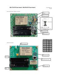
STD-302N-R 429MHz Operation Guide - Circuit Design, Inc.
STD-302N-R 429MHz Operation Guide - Circuit Design, Inc.
STD-302N-R 429MHz Operation Guide - Circuit Design, Inc.

You also want an ePaper? Increase the reach of your titles
YUMPU automatically turns print PDFs into web optimized ePapers that Google loves.
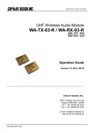
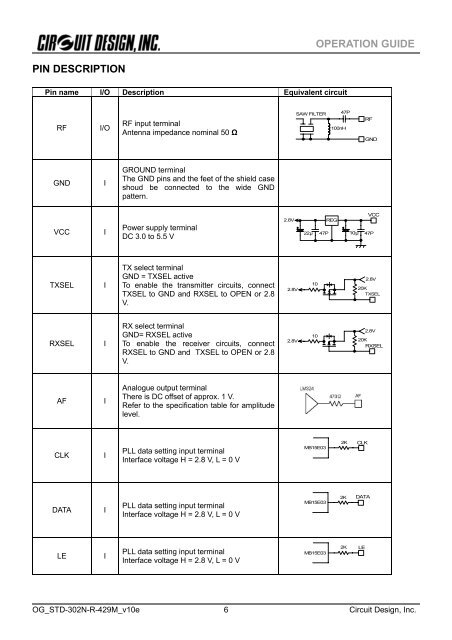
OPERATION GUIDE<br />
PIN DESCRIPTION<br />
Pin name I/O Description Equivalent circuit<br />
RF<br />
I/O<br />
RF input terminal<br />
Antenna impedance nominal 50 Ω<br />
SAW FILTER<br />
47P<br />
100nH<br />
RF<br />
GND<br />
GND<br />
I<br />
GROUND terminal<br />
The GND pins and the feet of the shield case<br />
shoud be connected to the wide GND<br />
pattern.<br />
VCC<br />
I<br />
Power supply terminal<br />
DC 3.0 to 5.5 V<br />
2.8V<br />
22µ 47P<br />
REG<br />
10µ<br />
VCC<br />
47P<br />
TXSEL<br />
I<br />
TX select terminal<br />
GND = TXSEL active<br />
To enable the transmitter circuits, connect<br />
TXSEL to GND and RXSEL to OPEN or 2.8<br />
V.<br />
2.8V<br />
10<br />
2.8V 20K<br />
TXSEL<br />
RXSEL<br />
I<br />
RX select terminal<br />
GND= RXSEL active<br />
To enable the receiver circuits, connect<br />
RXSEL to GND and TXSEL to OPEN or 2.8<br />
V.<br />
2.8V<br />
10<br />
2.8V 20K<br />
RXSEL<br />
AF<br />
I<br />
Analogue output terminal<br />
There is DC offset of approx. 1 V.<br />
Refer to the specification table for amplitude<br />
level.<br />
CLK<br />
I<br />
PLL data setting input terminal<br />
Interface voltage H = 2.8 V, L = 0 V<br />
MB15E03<br />
2K<br />
CLK<br />
DATA<br />
I<br />
PLL data setting input terminal<br />
Interface voltage H = 2.8 V, L = 0 V<br />
MB15E03<br />
2K<br />
DATA<br />
LE<br />
I<br />
PLL data setting input terminal<br />
Interface voltage H = 2.8 V, L = 0 V<br />
MB15E03<br />
2K<br />
LE<br />
OG_<strong>STD</strong>-<strong>302N</strong>-R-429M_v10e<br />
6<br />
<strong>Circuit</strong> <strong>Design</strong>, <strong>Inc</strong>.