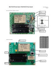
STD-302N-R 429MHz Operation Guide - Circuit Design, Inc.
STD-302N-R 429MHz Operation Guide - Circuit Design, Inc.
STD-302N-R 429MHz Operation Guide - Circuit Design, Inc.

Create successful ePaper yourself
Turn your PDF publications into a flip-book with our unique Google optimized e-Paper software.
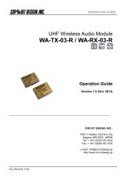
OPERATION GUIDE<br />
• Method of serial data input to the PLL<br />
After the RF channel table plan is decided, the data needs to be allocated to the ROM table and read from<br />
there or calculated with the software.<br />
Together with this setting data, operation bits that decide operation of the PLL must be sent to the PLL.<br />
The operation bits for setting the PLL are as follows. These values are placed at the head of the reference<br />
counter value and are sent to the PLL.<br />
1. CS: Charge pump current select bit<br />
CS = 0 +/-1.5 mA select VCO is optimized to +/-1.5 mA<br />
2. LDS: LD/fout output setting bit<br />
LDS = 0 LD select Hardware is set to LD output<br />
3. FC: Phase control bit for the phase comparator<br />
FC = 1<br />
Hardware operates at this phase<br />
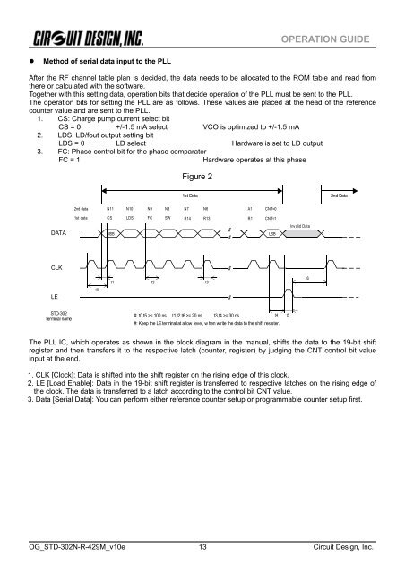
Figure 2<br />
1st Data<br />
2nd Data<br />
2nd data N11 N10 N9 N8 N7 N6 A1 CNT=0<br />
1st data<br />
CS<br />
LDS FC SW R14 R13 R1 CNT=1<br />
DATA<br />
MSB<br />
LSB<br />
Invalid Data<br />
CLK<br />
t1<br />
t2<br />
t3<br />
t6<br />
LE<br />
t0<br />
<strong>STD</strong>-302<br />
terminal name<br />
#: t0,t5 >= 100 ns t1,t2,t6 >= 20 ns t3,t4 >= 30 ns<br />
t4<br />
#: Keep the LE terminal at a low level, w hen w rite the data to the shift resister.<br />
t5<br />
The PLL IC, which operates as shown in the block diagram in the manual, shifts the data to the 19-bit shift<br />
register and then transfers it to the respective latch (counter, register) by judging the CNT control bit value<br />
input at the end.<br />
1. CLK [Clock]: Data is shifted into the shift register on the rising edge of this clock.<br />
2. LE [Load Enable]: Data in the 19-bit shift register is transferred to respective latches on the rising edge of<br />
the clock. The data is transferred to a latch according to the control bit CNT value.<br />
3. Data [Serial Data]: You can perform either reference counter setup or programmable counter setup first.<br />
OG_<strong>STD</strong>-<strong>302N</strong>-R-429M_v10e<br />
13<br />
<strong>Circuit</strong> <strong>Design</strong>, <strong>Inc</strong>.