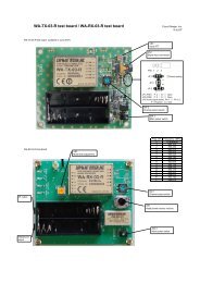
STD-302N-R 429MHz Operation Guide - Circuit Design, Inc.
STD-302N-R 429MHz Operation Guide - Circuit Design, Inc.
STD-302N-R 429MHz Operation Guide - Circuit Design, Inc.

Create successful ePaper yourself
Turn your PDF publications into a flip-book with our unique Google optimized e-Paper software.
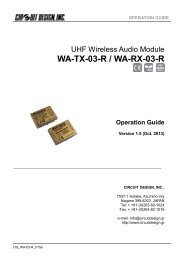
OPERATION GUIDE<br />
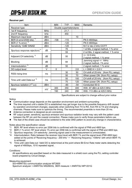
Receiver part<br />
Item MIN TYP MAX Remarks<br />
Receiver type<br />
Double superheterodyne<br />
1st IF frequency MHz 21.7<br />
2nd IF frequency kHz 450<br />
Maximum input level dBm 10<br />
BER (0 error/2556 bits) *1 dBm -108 -115 PN 9 4800bps<br />
BER (1 % error) *2 dBm -120 PN 9 4800bps<br />
Sensitivity 12dB/ SINAD dBm -120 fm1 k/ dev 2 kHz CCITT<br />
Spurious response rejections *3 dB<br />
70 1 st Mix, 2 signal method, 1 % error<br />
55 2 nd Mix, 2 signal method, 1 % error<br />
Adjacent CH selectivity *3 dB 50<br />
+/- 12.5 kHz,<br />
2 signal method, 1 % error<br />
Blocking dB 84<br />
Jamming signal +/- 1MHz<br />
2 signal method, 1% error<br />
Intermodulation *4 dB 50 2 signal method, 1 % error<br />
DO output level V 0 2.8 L = GND H = 2.8 V<br />
RSSI rising time<br />
ms<br />
30 50 CH shift of 25 kHz (from PLL setup)<br />
50 70 When power ON (from PLL setup)<br />
50 100 CH shift of 25 kHz (from PLL setup)<br />
Time until valid Data-out *5 ms<br />
70 120 When power ON (from PLL setup)<br />
Spurious radiation (1 st Lo) dBm -60 -54 Conducted 50 Ω<br />
RSSI<br />
mV<br />
300 350 400 With -97 dBm at 429.5 MHz<br />
190 240 290 With -113 dBm at 429.5 MHz<br />
Specifications are subject to change without prior notice<br />
Notice<br />
• Communication range depends on the operation environment and ambient surrounding<br />
• The time required until a stable DO is established may get longer due to the possible frequency drift caused<br />
by operation environment changes, especially when switching from TX to RX, from RX to TX and changing<br />
channels. Please make sure to optimize the timing. The recommended preamble is more than 20 ms.<br />
• Antenna connection is designed as pin connection.<br />
• RF output power, sensitivity, spurious emission and spurious radiation levels may vary with the pattern used<br />
between the RF pin and the coaxial connection. Please make sure to verify those parameters before use.<br />
• The feet of the shield case should be soldered to the wide GND pattern to avoid any change in characteristics.<br />
Notes about the specification values<br />
*1 BER: RF level where no error per 2556 bits is confirmed with the signal of PN9 and 4800 bps.<br />
*2 BER (1 % error): RF level where 1% error per 2556 bits is confirmed with the signal of PN9 and 4800 bps.<br />
*3 Spurious response, CH selectivity: Jamming signal used in the measurement is unmodulated.<br />
*4 Intermodulation: Ratio between the receiver input level with BER 1% and the signal level (PN9 4800 bps)<br />
added at the points of 'Receiving frequency - 200 kHz ' + ' Receiving frequency -100kHz' with which BER 1%<br />
is achieved.<br />
*5 Time until valid Data-out: Valid DO is determined at the point where Bit Error Rate meter starts detecting the<br />
signal of 4800bps, 1010 repeated signal.<br />
Conditions:<br />
All specifications are specified based on the data measured in a shield room using the PLL setting controller<br />
board prepared by <strong>Circuit</strong> <strong>Design</strong>.<br />
Measuring equipment:<br />
SG=ANRITSU communication analyzer MT2605<br />
Spectrum analyzer = ANRITSU MS2663G, BER measure = ANRITSU MP1201G<br />
OG_<strong>STD</strong>-<strong>302N</strong>-R-429M_v10e<br />
5<br />
<strong>Circuit</strong> <strong>Design</strong>, <strong>Inc</strong>.