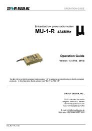
STD-302N-R 429MHz Operation Guide - Circuit Design, Inc.
STD-302N-R 429MHz Operation Guide - Circuit Design, Inc.
STD-302N-R 429MHz Operation Guide - Circuit Design, Inc.

You also want an ePaper? Increase the reach of your titles
YUMPU automatically turns print PDFs into web optimized ePapers that Google loves.
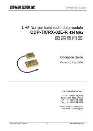
OPERATION GUIDE<br />
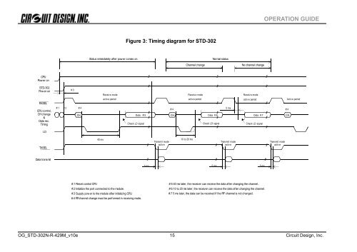
Figure 3: Timing diagram for <strong>STD</strong>-302<br />
Status immediately after pow er comes on.<br />
Normal status<br />
Channel change<br />
No channel change<br />
CPU<br />
Pow er on<br />
<strong>STD</strong>-302<br />
Pow er on<br />
RXSEL<br />
#:3<br />
Receive mode<br />
activ e period<br />
Receiv e mode<br />
activ e period<br />
Receiv e mode<br />
active period<br />
Activ e period<br />
CPU control,<br />
CH change<br />
&<br />
Data rec.<br />
Timing<br />
#:1 #:2<br />
#:4<br />
CH Data #:5<br />
Check LD signal<br />
#:4<br />
CH<br />
Data #:6<br />
Check LD signal<br />
5 ms<br />
Data #:7<br />
Check LD signal<br />
#:4<br />
CH<br />
LD<br />
TXSEL<br />
40 ms<br />
Transmit mode<br />
activ e<br />
10 to 20 ms<br />
Transmit mode<br />
activ e<br />
Transmit mode<br />
activ e<br />
Data transmit<br />
5 ms 5 ms<br />
5 ms<br />
#:1 Reset control CPU<br />
#:2 Initialize the port connected to the module.<br />
#:3 Supply pow er to the module after initializing CPU.<br />
#:4 RFchannel change must be performed in receiving mode.<br />
#:5 40 ms later, the receiver can receive the data after changing the channel..<br />
#:6 10 to 20 ms later, the receiver can receive the data after changing the channel.<br />
#:7 5 ms later, the data can be received if the RF channel is not changed.<br />
OG_<strong>STD</strong>-<strong>302N</strong>-R-429M_v10e 15<br />
<strong>Circuit</strong> <strong>Design</strong>, <strong>Inc</strong>.