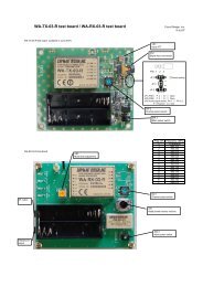
STD-302N-R 429MHz Operation Guide - Circuit Design, Inc.
STD-302N-R 429MHz Operation Guide - Circuit Design, Inc.
STD-302N-R 429MHz Operation Guide - Circuit Design, Inc.

You also want an ePaper? Increase the reach of your titles
YUMPU automatically turns print PDFs into web optimized ePapers that Google loves.
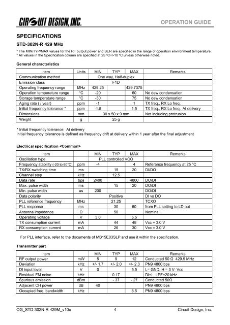
SPECIFICATIONS<br />
<strong>STD</strong>-<strong>302N</strong>-R 429 MHz<br />
OPERATION GUIDE<br />
* The MIN/TYP/MAX values for the RF output power and BER are specified in the range of operation environment temperature.<br />
* All values in the Specification column are specified at 25 ºC+/-10 ºC unless otherwise noted.<br />
General characteristics<br />
Item Units MIN TYP MAX Remarks<br />
Communication method<br />
One way, Half-duplex<br />
Emission class<br />
F1D<br />
Operating frequency range MHz 429.25 429.7375<br />
<strong>Operation</strong> temperature range °C -20 60 No dew condensation<br />
Storage temperature range °C -30 75 No dew condensation<br />
Aging rate ( / year) ppm -1 1 TX freq., RX Lo freq.<br />
Initial frequency tolerance * ppm -1.5 1.5 TX freq., RX Lo freq. At delivery<br />
Dimensions mm 30 x 50 x 9 mm Not including protrusion<br />
Weight g 25 g<br />
* Initial frequency tolerance: At delivery<br />
Initial frequency tolerance is defined as frequency drift at delivery within 1 year after the final adjustment<br />
Electrical specification <br />
Item MIN TYP MAX Remarks<br />
Oscillation type<br />
PLL controlled VCO<br />
Frequency stability (-20 to 60°C) ppm -4 4 Reference frequency at 25 °C<br />
TX/RX switching time ms 15 20 DI/DO<br />
Channel step kHz 12.5<br />
Data rate bps 2400 4800 DO/DI<br />
Max. pulse width ms 15 20 DO/DI<br />
Min. pulse width us 200 DO/DI<br />
Data polarity Positive DI vs DO<br />
PLL reference frequency MHz 21.25 TCXO<br />
PLL response ms 30 60 from PLL setting to LD out<br />
Antenna impedance Ω 50 Nominal<br />
Operating voltage V 3.0 5.5<br />
TX consumption current mA 44 48 Vcc = 3.0 V<br />
RX consumption current mA 26 30 Vcc = 3.0 V<br />
For PLL interface, refer to the documents of MB15E03SLP and use it within the specification.<br />
Transmitter part<br />
Item MIN TYP MAX Remarks<br />
RF output power mW 5 9 12 Conducted 50 Ω 429.5 MHz<br />
Deviation kHz +/- 1.7 +/- 2.0 +/- 2.3 PN9 4800 bps<br />
DI input level V 0 5.5 L= GND, H = 3 V- Vcc<br />
Residual FM noise kHz 0.17 DI=L, LPF=20 kHz<br />
Spurious emission dBm - 37 - 27 Conducted 50Ω<br />
Adjacent CH power dB 40 PN9 4800 bps<br />
Occupied freq. bandwidth kHz 8.5 PN9 4800 bps<br />
OG_<strong>STD</strong>-<strong>302N</strong>-R-429M_v10e<br />
4<br />
<strong>Circuit</strong> <strong>Design</strong>, <strong>Inc</strong>.