48~chapter 10 bscan
48~chapter 10 bscan
48~chapter 10 bscan

Create successful ePaper yourself
Turn your PDF publications into a flip-book with our unique Google optimized e-Paper software.
VLSI Test Principles and Architectures Ch. <strong>10</strong> – Boundary Scan & Core-Based Testing – P. 1/<strong>10</strong><br />
Chapter <strong>10</strong> Exercise Solutions<br />
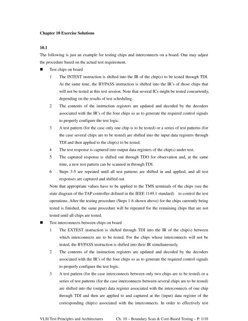
<strong>10</strong>.1<br />
The following is just an example for testing chips and interconnects on a board. One may adjust<br />
the procedure based on the actual test requirement.<br />
Test chips on board<br />
1 The INTEST instruction is shifted into the IR of the chip(s) to be tested through TDI.<br />
At the same time, the BYPASS instruction is shifted into the IR’s of those chips that<br />
will not be tested at this test session. Note that several ICs might be tested concurrently,<br />
depending on the results of test scheduling.<br />
2 The contents of the instruction registers are updated and decoded by the decoders<br />
associated with the IR’s of the four chips so as to generate the required control signals<br />
to properly configure the test logic.<br />
3 A test pattern (for the case only one chip is to be tested) or a series of test patterns (for<br />
the case several chips are to be tested) are shifted into the input data registers through<br />
TDI and then applied to the chip(s) to be tested.<br />
4 The test response is captured into output data registers of the chip(s) under test.<br />
5 The captured response is shifted out through TDO for observation and, at the same<br />
time, a new test pattern can be scanned in through TDI.<br />
6 Steps 3-5 are repeated until all test patterns are shifted in and applied, and all test<br />
responses are captured and shifted out.<br />
Note that appropriate values have to be applied to the TMS terminals of the chips (see the<br />
state diagram of the TAP controller defined in the IEEE 1149.1 standard) to control the test<br />
operations. After the testing procedure (Steps 1-6 shown above) for the chips currently being<br />
tested is finished, the same procedure will be repeated for the remaining chips that are not<br />
tested until all chips are tested.<br />
Test interconnects between chips on board<br />
1 The EXTEST instruction is shifted through TDI into the IR of the chip(s) between<br />
which interconnects are to be tested. For the chips whose interconnects will not be<br />
tested, the BYPASS instruction is shifted into their IR simultaneously.<br />
2 The contents of the instruction registers are updated and decoded by the decoders<br />
associated with the IR’s of the four chips so as to generate the required control signals<br />
to properly configure the test logic.<br />
3 A test pattern (for the case interconnects between only two chips are to be tested) or a<br />
series of test patterns (for the case interconnects between several chips are to be tested)<br />
are shifted into the (output) data register associated with the interconnects of one chip<br />
through TDI and then are applied to and captured at the (input) data register of the<br />
corresponding chip(s) associated with the interconnects. In order to effectively test
VLSI Test Principles and Architectures Ch. <strong>10</strong> – Boundary Scan & Core-Based Testing – P. 2/<strong>10</strong><br />
interconnects, specific test patterns such as walking one or walking zero sequences can<br />
be used. The details of these sequences can be found in [1].<br />
4 The captured response is shifted out through TDO for observation and, at the same<br />
time, a new test pattern can be scanned in through TDI.<br />
5 Steps 3-5 are repeated until all test patterns are shifted in and applied, and all test<br />
responses are captured and shifted out.<br />
Again, appropriate values have to be applied to the TMS terminals such that the test<br />
procedure can be executed correctly. Similar test procedures can be applied to the chips to<br />
test other interconnects.<br />
<strong>10</strong>.2<br />
The following calculation is based on the TAP controller state diagram shown in Figure <strong>10</strong>.7. The<br />
number of required test cycles to shift a 4-bit test instruction into the Instruction Register will be<br />
1 (to run-test/idle) +<br />
1 (to Select-DR-Scan) +<br />
1 (to Select-IR-Scan) +<br />
1 (to Capture-IR) +<br />
1 (to Shift-IR)*4 +<br />
1 (to Exit1-IR) +<br />
1 (to Exit2-IR) +<br />
1 (to update-IR) +<br />
1 (to Select-DR-Scan) = 12<br />
<strong>10</strong>.3<br />
Assume the initial state of TAP is Select-DR-Scan and the number of input wrapper cells equals<br />
that of output wrapper cells. The number of required test cycles to apply test patterns and<br />
propagate test responses is calculated as follows.<br />
The number of required test cycles to apply a test pattern is<br />
1 (to Capture-DR) +<br />
1 (to Shift-DR)*15 +<br />
1 (to Exit1-DR) +<br />
1 (to Update-DR) +<br />
1 (to Select-DR-Scan) = 19<br />
The number of required test cycles to observe test responses is<br />
1 (to Capture-DR) +<br />
1 (to Shift-DR)*15 +<br />
1 (to Exit1-DR) +
VLSI Test Principles and Architectures Ch. <strong>10</strong> – Boundary Scan & Core-Based Testing – P. 3/<strong>10</strong><br />
1 (to Update-DR) +<br />
1 (to Select-DR-Scan) = 19<br />
Note that after the first test pattern is applied, applying test patterns and propagating test responses<br />
can be executed simultaneously. Therefore, the number of required test cycles to apply test<br />
patterns and propagate test responses will be<br />
19 (applying the first test pattern) + 19*99 (applying test patterns and propagating test responses)<br />
+ 19 (propagating the last test responses) + 1 (to Select-IR-Scan) + 1 (to Test-Logic-Reset) = 1921.<br />
<strong>10</strong>.4<br />
Yes. As described in this chapter, the SAMPLE operation can be completed by simply executing<br />
the Capture operation (on the rising edge of TCK in the Capture-DR state). While the PRELOAD<br />
instruction allows test data to be shifted into/out of the selected data register during the Shift-DR<br />
state without causing interference to the normal operation of the internal logic as shown in Figure<br />
<strong>10</strong>.<strong>10</strong>. The shifted data is then latched to the parallel output (R2) of the selected data registers (on<br />
the falling edge of TCK in the Update-DR controller state). Since the states used to perform the<br />
corresponding operations for these two instructions are not overlapped (i.e., Capture-DR state for<br />
SAMPLE and Shift-DR as well as Update-DR states for PRELOAD), these two instructions can<br />
be executed in one iteration of the seven states shown in the middle of Figure <strong>10</strong>.7.<br />
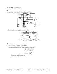
<strong>10</strong>.7<br />
The errors in Figure <strong>10</strong>.38 are the lack of the TMS control and a latch with negative level-sensitive<br />
nature as shown in following figure. Without fixing these two errors, the Init_Memory signal<br />
would not be activated before the occurrence of a transition in order to initialize the Hyst Mem in<br />
time, which is intended to guarantee that a valid transition can be captured for every test vector as<br />
described in the section pertaining IEEE 1149.6 Std.
VLSI Test Principles and Architectures Ch. <strong>10</strong> – Boundary Scan & Core-Based Testing – P. 4/<strong>10</strong><br />
○1 ○1<br />
○2<br />
<strong>10</strong>.8<br />
Based on the structure of digital driver logic defined in IEEE 1149.6 Std., one can derive the AC<br />
Test Signal in the timing diagram during EXTEST_PULSE instruction as shown in Figure <strong>10</strong>.20.<br />
Also the timing diagram during EXTEST_TRAIN instruction can be obtained in the same<br />
manner, as shown in the figure below [IEEE 1149.6-2003]. Clearly one can see that sequential<br />
transitions occur on the AC Test Signal line due to the EXTEST_TRAIN instruction when the TAP<br />
State is in Run-Test/Idle.
VLSI Test Principles and Architectures Ch. <strong>10</strong> – Boundary Scan & Core-Based Testing – P. 5/<strong>10</strong><br />
<strong>10</strong>.9<br />
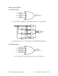
The gate-level netlist can be obtained by synthesizing the RTL codes (e.g., Verilog) that describe<br />
the functionalities of the wrapper cells using a commercial synthesis tool. Below are two<br />
schematics of the netllist for the two WBC’s.<br />
Gate-level netlist for <strong>10</strong>.26(a)<br />
Gate-level netlist for <strong>10</strong>.26(e)<br />
A comparison of functionalities, gate counts and control signals of these two cells is given in the<br />
table below.
VLSI Test Principles and Architectures Ch. <strong>10</strong> – Boundary Scan & Core-Based Testing – P. 6/<strong>10</strong><br />
functionalities gate counts control signals<br />
<strong>10</strong>.26(a) Shift and Capture 15<br />
ShiftWR, CaptureWR and<br />
mode<br />
<strong>10</strong>.26(e)<br />
Shift, Transfer, Update and<br />
ShiftWR, TransferDR,<br />
36<br />
Capture<br />
UpdateWR and CaptureWR<br />
<strong>10</strong>.<strong>10</strong><br />
Figure (a): WBR cell connectivity around a core
VLSI Test Principles and Architectures Ch. <strong>10</strong> – Boundary Scan & Core-Based Testing – P. 7/<strong>10</strong><br />
Figure (b): Delay test sequence timing diagram<br />
Figure (a) depicts a simplified example of an arrangement of an OR gate as a core and three<br />
WC_SD2_CIO cells (the structure is shown in Figure <strong>10</strong>.28) as WBR. The transfer, shift, and<br />
capture signals are derived from TransferDR, ShiftWR, and CaptureWR.<br />
Consider the scan order through 2 bits in each of the cells for terminals IN0, IN1, and OUT.<br />
The cell provided for terminal OUT is configured to receive the opposite polarity value of the<br />
IO_FACE signal from that applied to the other two cells. Also depicted are the logic values of a<br />
delay test of three vectors applied to the OR gate inside the simplified core.<br />
Figure (b) depicts a timing diagram of the delay test sequence. For ease of explanation, the<br />
rising edges of WRCK are numbered sequentially.<br />
The sequence begins with 6 data bits being shifted into the WBR. Following the Shift<br />
operation, data in dff_1 and dff_2 (see the structure in Figure <strong>10</strong>.28) of the wc_in0 wrapper cell are<br />
both 0; dff_1 and dff_2 of the wc_in1 cell are loaded with 1 and 0, respectively; data in dff_1 and<br />
dff_2 of the wc_out wrapper cell are both 0.<br />
With this data pattern, wc_in1 has an initial value of 0 applied, and there is a 1 value ready in<br />
that cell’s dff_1 storage element.<br />
Clock cycle 7 is a Transfer event where wc_in0 and wc_in1 internally exchange data between<br />
their respective dff_1 and dff_2 bits. This causes a rising-edge delay test stimulus being applied to<br />
the IN1 input of the OR gate.<br />
Clock cycle 8 performs both the Transfer and Capture events. If the time interval between<br />
clock events 7 and 8 is according to the delay time specification of the path from IN1 to OUT, then<br />
a first delay test response is captured in dff_2 of wc_out. Simultaneously, a falling-edge delay test<br />
stimulus is applied to the IN1 input of the OR gate. After a settling time, the WBR Test Output TO<br />
reflects the result of the capture.<br />
Clock cycle 9 again performs both the Transfer and Capture events. If the time interval
VLSI Test Principles and Architectures Ch. <strong>10</strong> – Boundary Scan & Core-Based Testing – P. 8/<strong>10</strong><br />
between clocks 8 and 9 is according to the delay specification of the OR gate a second delay test<br />
response is captured in dff_2 of wc_out. Simultaneously, the data value that was captured during<br />
clock 8 is transferred to dff_1 of wc_out. After a settling time, the WBR TO reflects the results of<br />
the second capture.<br />
Clocks <strong>10</strong> through 14 are used to shift out the last 5 bits of the WBR where the results of the<br />
first capture come out on clock <strong>10</strong>.<br />
Since the architecture of the standardized boundary scan cell does not support the<br />
functionality of interchanging contents in the embedded flip-flops (update and capture flip-flops)<br />
and latency exist between some test operations (e.g., 2 and half cycles between update and<br />
capture), the test procedure for delay faults discussed here cannot be directly applied to a circuit in<br />
compliance with IEEE 1149.1 Std..<br />
<strong>10</strong>.11<br />
Assume the numbers of input wrapper cells and output wrapper cells are equal. Then the number<br />
of required test cycles can be calculated as follows.<br />
4 (loading instruction) +<br />
(15+1) (shift in the first test pattern to the wrapper chain and apply to the circuit) +<br />
(15+1)*99 (shift in the remaining test patterns to the wrapper chain and apply to the circuit as<br />
well as capture the test response and shift out the test responses) +<br />
15 (shift out the test response associated with the last test pattern) = 1619 (cycles)<br />
<strong>10</strong>.12<br />
Assumption:<br />
1) The numbers of input wrapper cells and output wrapper cells are equal.<br />
2) 5 among the <strong>10</strong> parallel TAM wires are for TAM in and the others are for TAM out.<br />
3) The test data (including test patterns and responses) as well as test instruction are<br />
transferred via parallel TAM.<br />
Calculation:<br />
Since we assume the test instruction is transferred via parallel TAM (see Assumption 3), only<br />
1 cycle is required for loading the 4-bit instruction. On the other hand, the number of required<br />
cycles to execute scan operation can be calculated as follows. By taking Assumptions 1) and 2)<br />
into consideration, 3 cycles are required to shift in the 15-bit sized input/output wrapper chain.<br />
Thus totally<br />
(3+1) (shift in the first test pattern to the wrapper chain and apply to the circuit) +<br />
(3+1)*99 (shift in the remaining test patterns to the wrapper chain and apply to the circuit as well<br />
as capture and shift out the test responses) +<br />
3 (shift out the test response associated with the last test pattern)
VLSI Test Principles and Architectures Ch. <strong>10</strong> – Boundary Scan & Core-Based Testing – P. 9/<strong>10</strong><br />
= 403 cycles are required for scan operations.<br />
As a result, a total of 404 cycles are needed.<br />
Test configuration<br />
W<br />
B<br />
R<br />
FI<br />
FO<br />
W<br />
B<br />
R<br />
TAM in 5 bits<br />
1 to 4 DeMux<br />
W<br />
B<br />
R<br />
W<br />
B<br />
R<br />
FI<br />
FI<br />
Core<br />
Test<br />
Enable<br />
FO<br />
FO<br />
W<br />
B<br />
R<br />
W<br />
B<br />
R<br />
4 to 1 Mux<br />
TAM out 5 bits<br />
WBY<br />
WIR<br />
WSC<br />
Note: some details not<br />
shown in this figure<br />
Note: we also have to add some instructions to decode the proper control signals for the mux,<br />
demux and WBRs selection.<br />
<strong>10</strong>.13<br />
1. Parallel Mode<br />
IEEE 1500 Std. can provide higher transfer capability than IEEE 1149.1 Std. via parallel<br />
mode, which is one of the remarkable advantages of IEEE 1500 Std. over IEEE 1149.1 Std.<br />
2. Extra Data/Control I/Os<br />
IEEE 1500 Std. assumes that control signals are generated by a mechanism defined by the<br />
user, while for IEEE 1149.1 Std. these control signals are generated by the TAP controller.<br />
Therefore, IEEE 1500 Std. has more optional I/Os and higher flexibility.<br />
3. FSM (TAP Controller)<br />
Control signals of IEEE 1149.1 Std. are generated by a FSM, and thus the latency between<br />
some operations is inevitable, making some delay test unable to be applied. However, for<br />
IEEE 1500 Std. the generation mechanism is dominated by the user. Therefore the latency<br />
between operations can be eliminated.<br />
4. Transfer mode<br />
IEEE 1500 Std. can preserve as many capture values as there are storage elements in the
VLSI Test Principles and Architectures Ch. <strong>10</strong> – Boundary Scan & Core-Based Testing – P. <strong>10</strong>/<strong>10</strong><br />
shift path. It also can provide sequential stimuli data by the transfer mode, enabling delay<br />
test.<br />
5. Latency between shift, capture, and update operations for IEEE 1149.1 Std. results in long<br />
test time and limits the capability of the support of delay test.<br />
6. Mandatory Instructions:<br />
EXTEST and BYPASS in 1149.1 are similar to WS_EXTEST and WS_BYPASS. However,<br />
a WP_INTEST instruction would be highly beneficial in reducing test time if a large number<br />
of test access lines are available for the WPP.<br />
Reference<br />
[1] A. Hassan, J. Rajski, and V. K. Agarwal, “Testing and Diagnosis of Interconnects Using<br />
Boundary Scan Architecture,” Proc. Int’l Test Conf. pp. 126-137, 1988.