MIXS on BepiColombo and its DEPFET based focal ... - MPG HLL
MIXS on BepiColombo and its DEPFET based focal ... - MPG HLL
MIXS on BepiColombo and its DEPFET based focal ... - MPG HLL

Create successful ePaper yourself
Turn your PDF publications into a flip-book with our unique Google optimized e-Paper software.
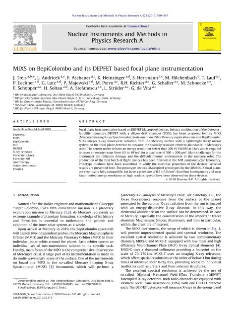
Nuclear Instruments <strong>and</strong> Methods in Physics Research A 624 (2010) 540–547<br />
C<strong>on</strong>tents lists available at ScienceDirect<br />
Nuclear Instruments <strong>and</strong> Methods in<br />
Physics Research A<br />
journal homepage: www.elsevier.com/locate/nima<br />
<str<strong>on</strong>g>MIXS</str<strong>on</strong>g> <strong>on</strong> <strong>BepiColombo</strong> <strong>and</strong> <strong>its</strong> <strong>DEPFET</strong> <strong>based</strong> <strong>focal</strong> plane instrumentati<strong>on</strong><br />
J. Treis a,b, , L. Andricek a,e , F. Aschauer a,c , K. Heinzinger a,d , S. Herrmann a,c , M. Hilchenbach b , T. Lauf a,c ,<br />
P. Lechner a,d , G. Lutz a,d , P. Majewski a,d , M. Porro a,c , R.H. Richter a,e , G. Schaller a,c , M. Schnecke a,e ,<br />
F. Schopper a,c , H. Soltau a,d , A. Stefanescu a,c , L. Strüder a,c , G. de Vita a,c<br />
a MPI Semic<strong>on</strong>ductor Laboratory, Otto-Hahn-Ring 6, 81739 Munich, Germany<br />
b MPI for Solar System Research, Max-Planck-Straße 2, 37191 Katlenburg-Lindau, Germany<br />
c MPI for Extraterrestrial Physics, Giessenbachstrasse, 85748 Garching, Germany<br />
d PNSensor GmbH, Römerstraße 28, 80803 Munich, Germany<br />
e MPI for Physics, Föhringer Ring 6, 80805 Munich, Germany<br />
article info<br />
Available <strong>on</strong>line 24 April 2010<br />
Keywords:<br />
<str<strong>on</strong>g>MIXS</str<strong>on</strong>g><br />
<strong>BepiColombo</strong><br />
IXO<br />
<strong>DEPFET</strong><br />
X-ray detectors<br />
Planetary science<br />
Planetary XRF<br />
Spectroscopy<br />
Active pixel sensor<br />
Imaging<br />
abstract<br />
Focal plane instrumentati<strong>on</strong> <strong>based</strong> <strong>on</strong> <strong>DEPFET</strong> Macropixel devices, being a combinati<strong>on</strong> of the Detector–<br />
Amplifier structure <strong>DEPFET</strong> with a silic<strong>on</strong> drift chamber (SDD), has been proposed for the <str<strong>on</strong>g>MIXS</str<strong>on</strong>g><br />
(Mercury Imaging X-ray Spectrometer) instrument <strong>on</strong> ESA’s Mercury explorati<strong>on</strong> missi<strong>on</strong> <strong>BepiColombo</strong>.<br />
<str<strong>on</strong>g>MIXS</str<strong>on</strong>g> images X-ray fluorescent radiati<strong>on</strong> from the Mercury surface with a lightweight X-ray mirror<br />
system <strong>on</strong> the <strong>focal</strong> plane detector to measure the spatially resolved element abundance in Mercury’s<br />
crust. The sensor needs to have an energy resoluti<strong>on</strong> better than 200 eV FWHM at 1 keV <strong>and</strong> is required<br />
to cover an energy range from 0.5 to 10 keV, for a pixel size of 300 300 mm 2 . Main challenges for the<br />
instrument are radiati<strong>on</strong> damage <strong>and</strong> the difficult thermal envir<strong>on</strong>ment in the mercury orbit. The<br />
producti<strong>on</strong> of the first batch of flight devices has been finished at the MPI semic<strong>on</strong>ductor laboratory.<br />
Prototype modules have been assembled to verify the electrical properties of the devices; selected<br />
results are presented here. The prototype devices, Macropixel prototypes for the SIMBOL-X <strong>focal</strong> plane,<br />
are electrically fully compatible, but have a pixel size of 0.5 0.5 mm 2 . Excellent homogeneity <strong>and</strong> near<br />
Fano-limited energy resoluti<strong>on</strong> at high readout speeds have been observed <strong>on</strong> these devices.<br />
& 2010 Elsevier B.V. All rights reserved.<br />
1. Introducti<strong>on</strong><br />
Named after the Italian engineer <strong>and</strong> mathematician Giuseppe<br />
‘‘Bepi’’ Colombo, ESA’s fifth cornerst<strong>on</strong>e missi<strong>on</strong> is a planetary<br />
explorati<strong>on</strong> missi<strong>on</strong> to Mercury [1,2]. As Mercury represents an<br />
extreme example of planetary formati<strong>on</strong>, knowledge of <strong>its</strong> history<br />
<strong>and</strong> formati<strong>on</strong> is essential to underst<strong>and</strong> the genesis <strong>and</strong><br />
evoluti<strong>on</strong> of the inner solar system as a whole.<br />
Up<strong>on</strong> arrival at Mercury in 2019, the <strong>BepiColombo</strong> spacecraft<br />
will deploy two independent probes, the Mercury Magnetospheric<br />
Orbiter (MMO) <strong>and</strong> the Mercury Planetary Orbiter (MPO) in their<br />
individual polar orb<strong>its</strong> around the planet. Each orbiter carries an<br />
individual set of instrumentati<strong>on</strong> tailored to <strong>its</strong> specific task.<br />
Hereby, main focus of the MPO is the comprehensive observati<strong>on</strong><br />
of Mercury’s crust. A large part of <strong>its</strong> instrumentati<strong>on</strong> is made to<br />
do multi-wavelength scans of the surface. One of the instruments<br />
<strong>on</strong> board the MPO is the so-called Mercury Imaging X-ray<br />
Spectrometer (<str<strong>on</strong>g>MIXS</str<strong>on</strong>g>) [3] instrument, which will perform a<br />
Corresp<strong>on</strong>ding author at: MPI Semic<strong>on</strong>ductor Laboratory, Otto-Hahn-Ring 6,<br />
81739 Munich, Germany. Tel.: +49 89 83940045; fax: +49 89 83940013.<br />
E-mail address: jft@hll.mpg.de (J. Treis).<br />
planetary XRF analysis of Mercury’s crust. For planetary XRF, the<br />
X-ray fluorescence resp<strong>on</strong>se from the surface of the planet<br />
generated by the cor<strong>on</strong>ar X-ray radiati<strong>on</strong> from the sun is imaged<br />
with an energy-dispersive X-ray detector. In this way, the<br />
elemental abundance <strong>on</strong> the surface can be determined. In case<br />
of Mercury, especially the c<strong>on</strong>centrati<strong>on</strong> of the important tracer<br />
elements Magnesium, Silic<strong>on</strong>, Aluminum, <strong>and</strong> Ir<strong>on</strong> in particular,<br />
within the crust are of interest.<br />
The <str<strong>on</strong>g>MIXS</str<strong>on</strong>g> instrument, the setup of which is shown in Fig. 1,<br />
will provide unprecedented spatial <strong>and</strong> spectral resoluti<strong>on</strong>. The<br />
excellent spatial resoluti<strong>on</strong> is achieved by two complementary<br />
channels, <str<strong>on</strong>g>MIXS</str<strong>on</strong>g>-C <strong>and</strong> <str<strong>on</strong>g>MIXS</str<strong>on</strong>g>-T, equipped with low mass <strong>and</strong> high<br />
efficiency Microchannel Plate (MCP) X-ray optical elements [4].<br />
<str<strong>on</strong>g>MIXS</str<strong>on</strong>g>-C uses a slumped collimator providing a footprint <strong>on</strong> the<br />
scale of 70–270 km. <str<strong>on</strong>g>MIXS</str<strong>on</strong>g>-T uses an imaging X-ray telescope,<br />
which offers spatial resoluti<strong>on</strong>s at the order of below 1 km during<br />
times of intensive solar X-ray flux, providing access to individual<br />
l<strong>and</strong>forms such as craters <strong>and</strong> their internal structures.<br />
The excellent spectral resoluti<strong>on</strong> is achieved by the use of<br />
so-called DEpleted P-channel Field-Effect Transistor (<strong>DEPFET</strong>)<br />
Macropixel X-ray detectors. Both <str<strong>on</strong>g>MIXS</str<strong>on</strong>g> channels are equipped with<br />
identical Focal Plane Assemblies (FPAs) with <strong>on</strong>e <strong>DEPFET</strong> detector<br />
each. The <strong>DEPFET</strong> detectors will measure X-rays in the energy b<strong>and</strong><br />
0168-9002/$ - see fr<strong>on</strong>t matter & 2010 Elsevier B.V. All rights reserved.<br />
doi:10.1016/j.nima.2010.03.173
J. Treis et al. / Nuclear Instruments <strong>and</strong> Methods in Physics Research A 624 (2010) 540–547 541<br />
<str<strong>on</strong>g>MIXS</str<strong>on</strong>g>-T<br />
FPAs<br />
Panel not shown<br />
<str<strong>on</strong>g>MIXS</str<strong>on</strong>g>-C<br />
Heat pipes coming<br />
from below<br />
MEB<br />
Fig. 1. Sketch of the <str<strong>on</strong>g>MIXS</str<strong>on</strong>g> instrument <strong>on</strong> <strong>BepiColombo</strong>. Two channels, <strong>on</strong>e equipped with a high resoluti<strong>on</strong> X-ray telescope <strong>and</strong> <strong>on</strong>e with a collimator optics, equipped with<br />
the same <strong>focal</strong> plane array, are located <strong>on</strong> a comm<strong>on</strong> panel (not shown), <strong>and</strong> their optics’ apertures facing the planet’s surface. They are c<strong>on</strong>trolled with a comm<strong>on</strong> readout<br />
electr<strong>on</strong>ics located in the <str<strong>on</strong>g>MIXS</str<strong>on</strong>g> electr<strong>on</strong>ics box (MEB). <str<strong>on</strong>g>MIXS</str<strong>on</strong>g>-C, the collimator instrument, serves for large scale observati<strong>on</strong>s of a large footprint in case of low solar<br />
X-ray intensity. <str<strong>on</strong>g>MIXS</str<strong>on</strong>g>-T, which requires higher solar X-ray fluxes, is used for imaging the fluorescence radiati<strong>on</strong> of the surface, capable of resolving features in the subkilometer<br />
range.<br />
of 0.5–7.5 keV with a spectral resoluti<strong>on</strong> 5100 eV FWHM at 1 keV<br />
at the start of operati<strong>on</strong>s <strong>and</strong> less than 200 eV at the end of the<br />
missi<strong>on</strong> lifetime, after two years in the Mercury orbit. This<br />
performance allows the separati<strong>on</strong> of X-ray line emissi<strong>on</strong> from<br />
elements of interest <strong>and</strong> provides access to lines not accessible to<br />
previous instruments, including the Fe-L emissi<strong>on</strong> lines.<br />
2. The <strong>DEPFET</strong> device<br />
The combined detector-amplifier structure DEpleted P-channel<br />
MOSFET (DEPMOSFET) [5,6] c<strong>on</strong>sists of a c<strong>on</strong>venti<strong>on</strong>al p-channel<br />
MOS-field effect transistor integrated <strong>on</strong> the surface of a high<br />
resistivity n-type silic<strong>on</strong> bulk. Using the principle of sidewards<br />
depleti<strong>on</strong> [7], the bulk can be fully depleted. By applying<br />
appropriate bias potentials to the fr<strong>on</strong>t- <strong>and</strong> backside, a potential<br />
minimum for electr<strong>on</strong>s can be generated near the surface of the<br />
bulk, <strong>and</strong> with an additi<strong>on</strong>al n-doped regi<strong>on</strong> this minimum can be<br />
enforced <strong>and</strong> c<strong>on</strong>fined to the area below the transistor channel.<br />
Bulk generated electr<strong>on</strong>–hole pairs are separated by the electric<br />
field <strong>and</strong> the electr<strong>on</strong>s are collected in the potential minimum<br />
below the transistor channel. Here, their presence modulates the<br />
charge carrier density in the channel, <strong>and</strong> the channel c<strong>on</strong>ductivity<br />
becomes a functi<strong>on</strong> of the charge in the potential minimum, which<br />
is therefore also referred to as internal gate. As the potential<br />
minimum is persistent regardless from the presence of a transistor<br />
current, the transistor can be turned off during signal integrati<strong>on</strong><br />
<strong>and</strong> <strong>on</strong>ly turned <strong>on</strong> for readout. The accumulated charge can be<br />
removed by applying a positive voltage pulse to an n + -doped regi<strong>on</strong><br />
close to the internal gate, the so-called clear-c<strong>on</strong>tact. The type of<br />
DEPMOSFET structures used for X-ray spectroscopy have circular<br />
transistor geometry. The clear regi<strong>on</strong> here c<strong>on</strong>sists of an additi<strong>on</strong>al<br />
N-MOSFET composed of the clear c<strong>on</strong>tact <strong>and</strong> a surrounding MOS<br />
structure, the so-called cleargate. The clear c<strong>on</strong>tact is separated from<br />
the detector bulk <strong>and</strong> the internal gate by an additi<strong>on</strong>al deep-p<br />
implantati<strong>on</strong>, to prevent charge loss to the clear. Fig. 2 shows a<br />
cutaway of a circular DEPMOSFET structure.<br />
During matrix operati<strong>on</strong>, the signal is evaluated by sampling<br />
the signal levels before <strong>and</strong> after the clear <strong>and</strong> calculating the<br />
difference, a technique usually referred to as correlated double<br />
sampling (CDS). As the clear is complete, the <strong>DEPFET</strong> is a kTCnoise<br />
free device. In large matrix devices, a pixel array is placed<br />
<strong>on</strong> a comm<strong>on</strong> bulk. As shown in Fig. 3, the pixels are interc<strong>on</strong>nected<br />
for row-wise, column-parallel readout in a rolling<br />
shutter mode.<br />
The <strong>DEPFET</strong> c<strong>on</strong>cept allows for more flexible interc<strong>on</strong>necti<strong>on</strong><br />
techniques, even pixel-individual addressing <strong>and</strong> readout are<br />
feasible in case sufficient routing resources are available. Small<br />
DEPMOSFET matrix prototypes of matrices of 64 64 pixel with<br />
75 75 mm 2 size each have successfully been operated <strong>and</strong> tested<br />
[8,9]. The <strong>DEPFET</strong>’s sensitivity is expressed as change in drainsource<br />
current as a functi<strong>on</strong> of the charge in the internal gate;<br />
g Q ¼ dI DS =dQ IG , which is a functi<strong>on</strong> of device geometry. The<br />
structures showing the best performance have a nominal gate<br />
width by design of 5 mm, the circular transistor gate has a<br />
circumference of 47:5 mm; g Q values of 350–500 pA/e have been<br />
measured, depending <strong>on</strong> the biasing c<strong>on</strong>diti<strong>on</strong>s. As the source<br />
follower c<strong>on</strong>versi<strong>on</strong> gain is given by dV S ¼ g Q =g m Q IG , gain<br />
values of 3:525 mV=e can be achieved. Operati<strong>on</strong> of a matrix<br />
device requires dedicated VLSI integrated c<strong>on</strong>trol <strong>and</strong> readout<br />
electr<strong>on</strong>ics. The c<strong>on</strong>trol-ICs used are the so-called SWITCHER II<br />
ICs [10], 64-channel dual high voltage multiplexer ICs manufactured<br />
in an AMS high voltage CMOS process. The Switchers drive<br />
the Gate, Cleargate <strong>and</strong> Clear voltages during operati<strong>on</strong>. The<br />
readout amplifier IC used is the ASTEROID 64 [11], a 64 channel<br />
shaper/amplifier circuit with a trapezoidal filtering stage, internal<br />
sample <strong>and</strong> hold, serial analog readout <strong>and</strong> integrated shaping<br />
sequencer allowing for flexible applicati<strong>on</strong> of different filter<br />
timing.<br />
3. <strong>DEPFET</strong> Macropixels<br />
When imaging X-ray wavelengths, the size of the PSF of the<br />
optics is typically in the range around 1 mm. C<strong>on</strong>sidering that<br />
charge sharing between pixels generally deteriorates the integral<br />
energy resoluti<strong>on</strong> due to recombinati<strong>on</strong> noise, the ideal pixel size<br />
is as small as necessary for reas<strong>on</strong>able oversampling of the PSF,<br />
but as large as possible to reduce charge sharing <strong>and</strong> power<br />
c<strong>on</strong>sumpti<strong>on</strong> by reducing the number of required readout<br />
channels. For an X-ray optical system with PSF around 1mm<br />
size, pixel sizes at the order of several hundreds of micr<strong>on</strong>s are<br />
desirable. <strong>DEPFET</strong> Macropixels [12] offer a c<strong>on</strong>venient way to<br />
adapt the pixel size to the requirement without sacrificing the<br />
excellent noise <strong>and</strong> energy resoluti<strong>on</strong> of the st<strong>and</strong>ard <strong>DEPFET</strong><br />
structure. By surrounding the <strong>DEPFET</strong> cell with an SDD-like<br />
drift ring structure [7] as shown in Fig. 4, the pixel size can be<br />
adapted to the requirements by simply changing number, size <strong>and</strong><br />
geometry of the drift electrodes. The resulting device, henceforth<br />
referred to as Macropixel, has the combined properties of <strong>DEPFET</strong><br />
<strong>and</strong> SDD:<br />
By changing number, geometry <strong>and</strong> size of the drift rings, any<br />
given pixel size can be implemented.
542<br />
J. Treis et al. / Nuclear Instruments <strong>and</strong> Methods in Physics Research A 624 (2010) 540–547<br />
75μm<br />
p+ drain<br />
polysilic<strong>on</strong><br />
gate<br />
p+ source<br />
polysilic<strong>on</strong><br />
cleargate<br />
n+ clear<br />
Fig. 2. Cutaway of a circular DEPMOSFET pixel device <strong>and</strong> the equivalent circuit schematics: A MOSFET with two gates: External <strong>and</strong> Internal Gate, while the latter can be<br />
c<strong>on</strong>tacted via the n-channel Clear-FET. A photo of a <strong>DEPFET</strong> structure inside a matrix is shown at the right.<br />
Fig. 3. Schematic interc<strong>on</strong>necti<strong>on</strong> of DEPMOSFET matrix pixels for row-wise readout. Row-wise c<strong>on</strong>necti<strong>on</strong> of Gate- <strong>and</strong> Clear-voltages provides for row addressing, <strong>and</strong><br />
column-wise c<strong>on</strong>necti<strong>on</strong> of the readout nodes provides for column-parallel readout.<br />
Placing an array of square-shaped Macropixel devices <strong>on</strong> a<br />
comm<strong>on</strong> bulk yields a large area FPA.<br />
Array readout in rolling shutter mode is possible due to the<br />
<strong>DEPFET</strong>’s charge storage capability.<br />
A Macropixel matrix is very power efficient, as the <strong>DEPFET</strong> is<br />
powered <strong>on</strong>ly in case it is actually read out.<br />
Like for any sideways depleted detector, the backside serves as<br />
radiati<strong>on</strong> entrance window <strong>and</strong> can be made completely
J. Treis et al. / Nuclear Instruments <strong>and</strong> Methods in Physics Research A 624 (2010) 540–547 543<br />
Fig. 4. Cross-cut through a Macropixel device. By replacing the readout anode of a c<strong>on</strong>venti<strong>on</strong>al SDD with a <strong>DEPFET</strong>, charge storage capability can be added to an SDD<br />
array. In this way, large integrating imaging detectors can be built from an array of Macropixels.<br />
homogeneous <strong>and</strong> unobstructed by any structure, yielding<br />
100% fill factor <strong>and</strong> extremely good quantum efficiency.<br />
Due to the low input capacitance of the <strong>DEPFET</strong>s, the devices<br />
can be read out very fast at low noise; readout noise values of<br />
4e ENC at a readout speed of o6 ms have been achieved,<br />
The radiati<strong>on</strong> hardness of the <strong>DEPFET</strong> technology has already<br />
been proven experimentally [13,14].<br />
These properties make <strong>DEPFET</strong> Macropixel matrix devices<br />
suitable for a large number of experiments. Single Macropixel<br />
prototypes from an earlier prototyping run have successfully<br />
tested <strong>and</strong> showed outst<strong>and</strong>ing performance in spite of the large<br />
pixel area [12].<br />
4. The <str<strong>on</strong>g>MIXS</str<strong>on</strong>g> <strong>focal</strong> plane detector<br />
Table 1 shows the key specificati<strong>on</strong>s <strong>on</strong> the <str<strong>on</strong>g>MIXS</str<strong>on</strong>g> FPA sensors.<br />
The sensitive area is made to match the mirror system field of<br />
view (FOV). The pixel size is achieved adopting a layout with three<br />
drift rings around a st<strong>and</strong>ard circular <strong>DEPFET</strong> structure. The<br />
quantum efficiency has been achieved with the st<strong>and</strong>ard radiati<strong>on</strong><br />
entrance window c<strong>on</strong>figurati<strong>on</strong> for the <strong>DEPFET</strong> technology. The<br />
time resoluti<strong>on</strong> is mostly driven by the spacecraft movement over<br />
ground, the pixel size of 300 300 mm 2 is designed to allow for<br />
3 fold oversampling of the optic’s 1 mm PSF. The energy range<br />
is selected to cover both the ir<strong>on</strong>-K line (6.4 keV) <strong>and</strong> the ir<strong>on</strong>-L<br />
lines ( 0:71 keV). Being sensitive perm<strong>its</strong> to detect ir<strong>on</strong> even in<br />
case of a quiet sun state, where both intensity <strong>and</strong> energy of the<br />
cor<strong>on</strong>ar X-rays are too low to generate a significant flux of Ir<strong>on</strong>-K<br />
phot<strong>on</strong>s. As a result, the ir<strong>on</strong> sensitivity is drastically increased.<br />
The energy resoluti<strong>on</strong> limit is very moderate, as well as the limit<br />
<strong>on</strong> the electr<strong>on</strong>ic noise. This is as the main task of the detector is<br />
to directly observe <strong>and</strong> separate the unaltered X-ray fluorescence<br />
spectral lines from the most important tracer elements <strong>on</strong> a<br />
background from bremsstrahlung <strong>and</strong> scattered radiati<strong>on</strong>, in<br />
c<strong>on</strong>trast to applicati<strong>on</strong>s in X-ray astr<strong>on</strong>omy, where both<br />
str<strong>on</strong>gly red- <strong>and</strong> blue-shifted emissi<strong>on</strong> lines have to be<br />
detected <strong>and</strong> separated from the background, a task which<br />
imposes much more dem<strong>and</strong>ing requirements <strong>on</strong> the energy<br />
resoluti<strong>on</strong>. The biggest challenge for the <str<strong>on</strong>g>MIXS</str<strong>on</strong>g> detector is the<br />
radiati<strong>on</strong> hardness. The main radiati<strong>on</strong> damage is caused by low<br />
energy prot<strong>on</strong>s from the solar wind. The expected threshold<br />
Table 1<br />
Requirements <strong>on</strong> the <strong>focal</strong> plane arrays of the <str<strong>on</strong>g>MIXS</str<strong>on</strong>g> instruments. The requirement<br />
<strong>on</strong> the FWHM at 1 keV allows for a much higher ENC, but the main source of<br />
energy resoluti<strong>on</strong> deteriorati<strong>on</strong> is due to leakage current increase.<br />
Parameter<br />
Requirement<br />
Sensitive area 1.92 1.92 cm 2<br />
Quantum efficiency<br />
Z80% at 0:5 keV<br />
Time resoluti<strong>on</strong><br />
o1ms<br />
Pixel size 300 300 mm 2<br />
Array dimensi<strong>on</strong><br />
64 64 pixels<br />
Energy resoluti<strong>on</strong><br />
200 eV FWHM at 1 keV<br />
Energy range<br />
0:5 keVZEZ10 keV<br />
Electr<strong>on</strong>ic noise (without o10e ENC<br />
leakage current)<br />
Leakage current induced o20e ENC<br />
noise c<strong>on</strong>tributi<strong>on</strong><br />
Radiati<strong>on</strong> hardness<br />
Z3 10 10 eq: 10 MeV p=cm 2 r20 krad TID<br />
voltage shift in the <strong>DEPFET</strong> gates [13] of below 0.7 V from the total<br />
i<strong>on</strong>izing dose (TID) of o20 krad can easily be compensated by<br />
adapting the operating c<strong>on</strong>diti<strong>on</strong>s. The expected increase of<br />
leakage current due to prot<strong>on</strong>-induced bulk damage (n<strong>on</strong>i<strong>on</strong>izing<br />
energy loss, NIEL), however, must be compensated by a<br />
faster readout speed <strong>and</strong> a corresp<strong>on</strong>dingly lower operating<br />
temperature, although the specificati<strong>on</strong>s allow for a relatively<br />
large leakage current induced noise c<strong>on</strong>tributi<strong>on</strong>. In a space<br />
envir<strong>on</strong>ment, applying annealing to the detector is an uncomm<strong>on</strong><br />
procedure due to the involved risks. Therefore, the detector will<br />
be mostly kept in the cooled state, <strong>and</strong> radiati<strong>on</strong> damage tests<br />
have been made to verify the damage c<strong>on</strong>stant in cold c<strong>on</strong>diti<strong>on</strong>s<br />
without self-annealing [14] <strong>and</strong> to estimate the effect of<br />
annealing vs. no annealing. Fig. 5 shows the extrapolated<br />
tradeoff between energy resoluti<strong>on</strong> after receiving the full<br />
missi<strong>on</strong> lifetime dose, readout speed <strong>and</strong> detector temperature,<br />
assuming an annealing scenario of 80 min at 60 1C (left), <strong>and</strong><br />
without applying any annealing at all (right). A frame integrati<strong>on</strong><br />
time of 192 ms corresp<strong>on</strong>ds to 6 ms readout time per row, which is<br />
the st<strong>and</strong>ard readout speed with the ASTEROID IC. For this<br />
integrati<strong>on</strong> time, an operating temperature of 43 1C is required<br />
to keep the energy resoluti<strong>on</strong> requirement. If the readout speed is<br />
increased to 128 ms, a temperature below 391C is sufficient, at<br />
the cost of higher initial readout noise due to the shorter shaping
544<br />
J. Treis et al. / Nuclear Instruments <strong>and</strong> Methods in Physics Research A 624 (2010) 540–547<br />
Integrati<strong>on</strong> time (µs)<br />
350<br />
300<br />
250<br />
200<br />
150<br />
100<br />
-43°C<br />
-39°C<br />
Energy resoluti<strong>on</strong><br />
FWHM @ 1 keV<br />
60.00<br />
100.0<br />
140.0<br />
180.0<br />
220.0<br />
260.0<br />
300.0<br />
White line:<br />
200 eV requirement<br />
Integrati<strong>on</strong> time (µs)<br />
350<br />
300<br />
250<br />
200<br />
150<br />
100<br />
-47°C<br />
-50°C<br />
Energy resoluti<strong>on</strong><br />
FWHM @ 1 keV<br />
60.00<br />
100.0<br />
140.0<br />
180.0<br />
220.0<br />
260.0<br />
300.0<br />
White line:<br />
200 eV requirement<br />
-30 -35 -40 -45 -50 -55 -60<br />
Temperature (°C)<br />
-30 -35 -40 -45 -50 -55 -60<br />
Temperature (°C)<br />
Fig. 5. Radiati<strong>on</strong> damage tradeoff for the <str<strong>on</strong>g>MIXS</str<strong>on</strong>g> <strong>focal</strong> plane detectors applying an annealing cycle of 80 min at 60 1C (left) <strong>and</strong> without applying any annealing (right). In<br />
case an annealing scenario is applied, an operati<strong>on</strong> temperature of, depending <strong>on</strong> the readout speed, 39243 3 C is required to fulfill the energy resoluti<strong>on</strong> requirement<br />
having received the full prot<strong>on</strong> dose at the end of the missi<strong>on</strong> lifetime. Without annealing, the required operating temperatures are significantly lower.<br />
Clear<br />
Switchers<br />
North<br />
ASTEROID<br />
Gate/<br />
Cleargate<br />
Switchers<br />
Northwest<br />
Switcher<br />
Northern<br />
hemisphere<br />
Northeast<br />
Switcher<br />
Fanouts<br />
Southern<br />
hemisphere<br />
Southwest<br />
Switcher<br />
Southeast<br />
Switcher<br />
W<br />
N<br />
E<br />
South<br />
ASTEROID<br />
S<br />
Fig. 6. Readout scheme of the FPA detectors for <str<strong>on</strong>g>MIXS</str<strong>on</strong>g> (left). The sensor is divided in two equally sized hemispheres of 32 64 pixels each, which are c<strong>on</strong>trolled <strong>and</strong> read out<br />
by an individual set of fr<strong>on</strong>t-end electr<strong>on</strong>ics. Photograph of a laboratory module for <str<strong>on</strong>g>MIXS</str<strong>on</strong>g> (mechanical sample) during integrati<strong>on</strong> (right). The overall sensor sensitive area<br />
is 1.92 1.92 cm 2 , the envelope size of the central regi<strong>on</strong> of the hybrid is 4 in. 4 in.<br />
time in the ASTEROID IC. If no annealing is provided, the operating<br />
temperatures have to be 8 3 C lower. As the cooling resources <strong>on</strong><br />
board of the <strong>BepiColombo</strong> spacecraft are very limited <strong>and</strong> even<br />
the less cold temperatures are hard to be achieved, annealing<br />
scenarios are being c<strong>on</strong>sidered in spite of the risk involved.<br />
Fig. 6 shows the structure <strong>and</strong> readout scheme for the <str<strong>on</strong>g>MIXS</str<strong>on</strong>g><br />
FPA sensors <strong>and</strong> a photo of a laboratory hybrid. The sensor is<br />
divided in two individual hemispheres of 64 32 pixels each,<br />
which are c<strong>on</strong>trolled <strong>and</strong> read out by their hemisphere-individual<br />
fr<strong>on</strong>t end electr<strong>on</strong>ics. For this c<strong>on</strong>figurati<strong>on</strong>, two rows can be read<br />
at the same time, which increases the achievable framerate by a<br />
factor of two, <strong>and</strong> <strong>on</strong>e degree of redundancy is added to the<br />
system. Every hemisphere is read <strong>and</strong> c<strong>on</strong>trolled by <strong>its</strong><br />
hemisphere-individual ASTEROID <strong>and</strong> Switcher circu<strong>its</strong>.<br />
The producti<strong>on</strong> of the flight detectors for <str<strong>on</strong>g>MIXS</str<strong>on</strong>g> has recently<br />
been finished at the MPI semic<strong>on</strong>ductor laboratory in Munich. The<br />
devices will undergo a test program <strong>on</strong> die level to select flight<br />
devices without cosmetic defects or inefficiencies prior to their<br />
integrati<strong>on</strong> into a laboratory or flight hybrid.<br />
5. Prototype tests<br />
To evaluate the prototypes <strong>and</strong> to learn about the properties of<br />
a Macropixel matrix device, even larger Macropixel detector<br />
prototypes with 64 64 pixels of a pixel size of 500 500 mm 2<br />
<strong>and</strong> an overall sensitive area of 3.2 3.2 cm 2 , being about three<br />
times the size of the <str<strong>on</strong>g>MIXS</str<strong>on</strong>g> Macropixel devices, have been
J. Treis et al. / Nuclear Instruments <strong>and</strong> Methods in Physics Research A 624 (2010) 540–547 545<br />
Fig. 7. Photos of fr<strong>on</strong>t- (left) <strong>and</strong> backside (top right) of a Macropixel matrix prototype, being an representative sample for the <str<strong>on</strong>g>MIXS</str<strong>on</strong>g> detectors. The overall sensor sensitive<br />
area is 3.2 3.2 cm 2 , the envelope size of the hybrid is 4 in. 4 in. The pixel array dimensi<strong>on</strong> is 64 64 <strong>and</strong> the pixels (bottom right) have five drift rings each <strong>and</strong> a size of<br />
500 500 mm 2 . The pixel structure <strong>and</strong> the c<strong>on</strong>trol- <strong>and</strong> read-out electr<strong>on</strong>ics <strong>on</strong> the fr<strong>on</strong>tside is clearly visible, as well as the completely homogeneous entrance window <strong>on</strong><br />
the backside.<br />
60<br />
Offset (ADU)<br />
50<br />
2600<br />
Row number<br />
60<br />
50<br />
40<br />
30<br />
20<br />
Noise<br />
(ADURMS)<br />
10.00<br />
11.00<br />
12.00<br />
13.00<br />
14.00<br />
15.00<br />
16.00<br />
17.00<br />
18.00<br />
19.00<br />
20.00<br />
Row number<br />
40<br />
30<br />
20<br />
10<br />
60<br />
50<br />
10 20 30 40 50 60<br />
Columnnumber<br />
2800<br />
3000<br />
3200<br />
3400<br />
3600<br />
Residual<br />
Offset (A DU)<br />
10<br />
10 20 30 40 50 60<br />
Column number<br />
Row number<br />
40<br />
30<br />
20<br />
-500.0<br />
-300.0<br />
-100.0<br />
100.0<br />
300.0<br />
10<br />
10 20 30 40 50 60<br />
Columnnumber<br />
Fig. 8. Offset (right) <strong>and</strong> noise (left) map of the tested Macropixel device. The offset map entries are the mean values of typically 1000 offset values per pixel, the noise<br />
map values are their variances. The column-like structure <strong>on</strong> the offset map (top right) is due to the ASTEROID’s channel-to-channel offset variati<strong>on</strong>, the sensor <strong>its</strong>elf shows<br />
in the residual offset map (bottom right) no bright pixels at all, <strong>and</strong> no systematic variati<strong>on</strong>, except for a slightly higher offset values at the edges, which is due to thermal<br />
reas<strong>on</strong>s. The noise map is also very homogeneous, the noise dispersi<strong>on</strong> is at the order of 7%. The mean value of the noise map entries translates in an ENC value of<br />
4.1e rms. The slightly higher noise at the bottom sensor rim is due to additi<strong>on</strong>al thermal load from the fr<strong>on</strong>t end ICs.<br />
successfully taken into operati<strong>on</strong> <strong>and</strong> have been tested. These<br />
devices, originally being manufactured as prototypes for the<br />
SIMBOL-X <strong>focal</strong> plane [15], have the identical pixel structure <strong>and</strong><br />
array dimensi<strong>on</strong> compared to the <str<strong>on</strong>g>MIXS</str<strong>on</strong>g> detectors, but the pixels<br />
have five drift rings instead of three to cover the larger active area.<br />
In additi<strong>on</strong>, the sensor is not divided into hemispheres. As the
546<br />
J. Treis et al. / Nuclear Instruments <strong>and</strong> Methods in Physics Research A 624 (2010) 540–547<br />
scaling behavior of the drift ring structure is very well known,<br />
the prototypes are being c<strong>on</strong>sidered as representative samples for<br />
<str<strong>on</strong>g>MIXS</str<strong>on</strong>g>. The sensors also possess the same entrance window<br />
c<strong>on</strong>figurati<strong>on</strong>. Fig. 7 shows photographs of the sensors fr<strong>on</strong>t<strong>and</strong><br />
backside, <strong>and</strong> of the pixel structure <strong>its</strong>elf. The completely<br />
homogeneous aluminized entrance window can be recognized, as<br />
well as the pixel structure <strong>on</strong> the fr<strong>on</strong>tside, together with the two<br />
c<strong>on</strong>trol-ICs <strong>and</strong> the ASTEROID IC. The overall hybrid size is<br />
4 in. 4 in. A total number of five hybrids of that type was built.<br />
Three devices were homogeneous <strong>and</strong> defect-free, <strong>on</strong>e had <strong>on</strong>ly<br />
<strong>on</strong>e defective row, <strong>and</strong> <strong>on</strong>ly <strong>on</strong>e structure had a larger number of<br />
defective pixels. Given the larger area of the devices compared to<br />
the <str<strong>on</strong>g>MIXS</str<strong>on</strong>g> flight detectors, a producti<strong>on</strong> yield of around 70% can be<br />
expected.<br />
The sensors have been tested in a vacuum envir<strong>on</strong>ment<br />
at a relatively low sensor temperature around 90 1C, with a<br />
18000<br />
16000<br />
10000<br />
14000<br />
12000<br />
1000<br />
Pattern multiplicity<br />
Singles<br />
Doubles<br />
Triples<br />
Quadruples<br />
Counts<br />
10000<br />
8000<br />
6000<br />
4000<br />
Counts<br />
100<br />
2000<br />
0<br />
5600 5800 6000 6200 6400 6600 6800 7000<br />
Energy(eV)<br />
14000<br />
12000<br />
10<br />
10000<br />
1<br />
1000 2000 3000 4000 5000 6000 7000 8000<br />
Energy(eV)<br />
Counts<br />
8000<br />
6000<br />
4000<br />
2000<br />
0<br />
5600 5800 6000 6200 6400 6600 6800 7000<br />
Energy(eV)<br />
Fig. 9. Sample spectra taken with the Macropixel array using an 55 Fe source. No inefficient pixels were found. The left figure shows the spectra for the various multiplicities<br />
(gray coded), the right figures show the peak regi<strong>on</strong> for the singles spectrum <strong>and</strong> the integral spectrum taking into account all multiplicities. The energy resoluti<strong>on</strong><br />
measured was 126 eV FWHM at 5.9 keV taking <strong>on</strong>ly singles, i.e. events without charge sharing, <strong>and</strong> 128 eV FWHM taking all valid event patterns, which is in agreement<br />
with the expectati<strong>on</strong>s. The peak to background ratio of 3000 shows the suitability of the devices for spectroscopic measurements.<br />
60<br />
60<br />
Row number<br />
50<br />
40<br />
30<br />
20<br />
10.00<br />
133.8<br />
257.5<br />
381.3<br />
505.0<br />
628.8<br />
752.5<br />
876.3<br />
1000<br />
Row number<br />
50<br />
40<br />
30<br />
20<br />
10.00<br />
133.8<br />
257.5<br />
381.3<br />
505.0<br />
628.8<br />
752.5<br />
876.3<br />
1000<br />
10<br />
10<br />
10 20 30 40 50 60<br />
Column number<br />
10 20 30 40 50 60<br />
Column number<br />
Fig. 10. Imaging test using an silic<strong>on</strong> baffle of 0.45 mm thickness. The smallest feature size is 0.4 mm. The left image shows an intensity plot (phot<strong>on</strong>s per pixel), the right<br />
image an extrapolated c<strong>on</strong>tour plot.
J. Treis et al. / Nuclear Instruments <strong>and</strong> Methods in Physics Research A 624 (2010) 540–547 547<br />
framerate of around 2.5 kHz. For <str<strong>on</strong>g>MIXS</str<strong>on</strong>g>, the framerate will be by a<br />
factor of two higher, the integrati<strong>on</strong> time will be r200 ms. As<br />
can be seen from Fig. 8, the sensor shows excellent homogeneity<br />
<strong>and</strong> noise. The visible structures in the offset <strong>and</strong> noise maps<br />
are due to the ASTEROID channel-to-channel offset. The noise<br />
distributi<strong>on</strong> is very flat, no noisy pixels have been observed.<br />
The noise dispersi<strong>on</strong> of 7% is due to pixels close to the sensor rim<br />
at the bottom having a slightly higher noise. This is caused by the<br />
proximity of the ASTEROID IC inducing additi<strong>on</strong>al heat load,<br />
probably in form of infrared radiati<strong>on</strong>.<br />
The sensors have been exposed to an 55 Fe source. The devices<br />
show excellent spectral resoluti<strong>on</strong>. The resulting spectra are<br />
shown in Fig. 9. The energy resoluti<strong>on</strong> is with 126 eV FWHM at<br />
5.9 keV close to the Fano limit, <strong>and</strong> the slightly worse energy<br />
resoluti<strong>on</strong> of the integral spectra taking into account also spl<strong>its</strong>, is<br />
with 128 eV within the expectati<strong>on</strong>s. The overlay of the spectra of<br />
the various multiplicities gives an impressi<strong>on</strong> of the quality of the<br />
gathered spectra. 76.9% of the recorded patterns are singles, 20.6%<br />
are doubles <strong>and</strong> the remaining 2.5% distribute evenly am<strong>on</strong>g<br />
triples <strong>and</strong> quadruples, a split behavior which is in agreement<br />
with the simulati<strong>on</strong>s. The peak-to background ratio of C3000<br />
qualifies the devices as suitable for spectroscopy applicati<strong>on</strong>s <strong>and</strong><br />
is a proof of the good quality of the entrance window.<br />
Imaging tests have been d<strong>on</strong>e using a 450 mm thick silic<strong>on</strong><br />
baffle. The resulting images are shown in Fig. 10. the smallest<br />
feature size for this baffle was 0.4 mm. Although a quantitative<br />
analysis using MTF structures still need to be d<strong>on</strong>e, these images<br />
give an impressi<strong>on</strong> of the homogeneity <strong>and</strong> excellent imaging<br />
properties of the sensors.<br />
6. Summary <strong>and</strong> outlook<br />
<strong>DEPFET</strong> <strong>based</strong> Macropixel detectors have been designed<br />
<strong>and</strong> produced for the <strong>focal</strong> plane instrumentati<strong>on</strong> of the <str<strong>on</strong>g>MIXS</str<strong>on</strong>g><br />
spectrometer <strong>on</strong> board <strong>BepiColombo</strong>’s MPO. The devices are in the<br />
process of being die-tested for flight qualificati<strong>on</strong>. Prototypes of<br />
even larger area <strong>and</strong> pixel sizes have been successfully taken into<br />
operati<strong>on</strong>. The tested devices are homogeneous <strong>and</strong> defect free<br />
<strong>and</strong> show excellent imaging <strong>and</strong> spectroscopic properties.<br />
As so<strong>on</strong> as the die testing is finished, device qualificati<strong>on</strong> will<br />
c<strong>on</strong>tinue with quantitative testing of the imaging properties, a<br />
quantitative analysis of the entrance window quantum efficiency<br />
<strong>and</strong> the radiati<strong>on</strong> hardness of the device to c<strong>on</strong>firm the results of<br />
the diode test irradiati<strong>on</strong>. The radiati<strong>on</strong> qualificati<strong>on</strong> of the<br />
ASTEROID <strong>and</strong> SWITCHER ICs is also a matter of c<strong>on</strong>cern.<br />
In additi<strong>on</strong>, prototype devices have been taken to the BESSY II<br />
beamline at the PTB facility in Berlin, Germany, for calibrati<strong>on</strong><br />
purposes. The calibrated sensors are going to be used for X-ray<br />
fluorescence analysis measurements <strong>on</strong> Ir<strong>on</strong> samples at the<br />
ELETTRA synchrotr<strong>on</strong> facility in Trieste, Italy.<br />
References<br />
[1] R. Grard, et al., ESA Bulletin 103 (2000) 11.<br />
[2] A. Anselmi, G.E.N. Sco<strong>on</strong>, Planetary <strong>and</strong> Space Science 49 (2001) 1409.<br />
[3] G.W. Fraser, et al., Planetary <strong>and</strong> Space Science 58 (1-2) (2010) 79, doi:10.1016/j.<br />
pss.2009.05.004.<br />
[4] G.W. Fraser, et al., Nucl. Instr. <strong>and</strong> Meth. A 324 (1993) 404.<br />
[5] J. Kemmer, G. Lutz, Nucl. Instr. <strong>and</strong> Meth. A 253 (1987) 356.<br />
[6] J. Treis, et al., <strong>DEPFET</strong> <strong>based</strong> <strong>focal</strong> plane instrumentati<strong>on</strong> for X-ray imaging<br />
spectroscopy in space, in: IEEE NSS C<strong>on</strong>ference Record 2007, IEEE Nuclear<br />
Science Symposium C<strong>on</strong>ference Record, 2007, p. N47-3.<br />
[7] E. Gatti, P. Rehak, Nucl. Instr. <strong>and</strong> Meth. A 225 (1984) 608.<br />
[8] J. Treis, et al., Nucl. Instr. <strong>and</strong> Meth. A 568 (2006) 191.<br />
[9] J. Treis, et al., IEEE Trans. Nucl. Sci. NS-52 (2005) 1083.<br />
[10] J. Treis, et al., First results of <strong>DEPFET</strong> <strong>based</strong> active pixel sensor prototypes for<br />
the XEUS wide field imager, in: A.D. Holl<strong>and</strong> (Ed.), High-Energy Detectors in<br />
Astr<strong>on</strong>omy, SPIE Proceedings, vol. 5501, 2004, pp. 89–100.<br />
[11] M. Porro, et al., Performance of ASTEROID: a 64 Channel ASIC for source<br />
follower readout of <strong>DEPFET</strong> matrices for X-ray astr<strong>on</strong>omy, IEEE NSS<br />
C<strong>on</strong>ference Record 2008, in: IEEE Nuclear Science Symposium C<strong>on</strong>ference<br />
Record, 2008, p. N23-6.<br />
[12] C. Zhang, et al., Nucl. Instr. <strong>and</strong> Meth. A 568 (2006) 207.<br />
[13] L. Andricek, et al., Radiati<strong>on</strong> tolerance of the MOS-Type <strong>DEPFET</strong> active pixel<br />
sensor, in: IEEE NSS C<strong>on</strong>ference Record 2007, IEEE Nuclear Science<br />
Symposium C<strong>on</strong>ference Record, 2007, p. N16-6.<br />
[14] G. Segneri, et al., Measurement of the current related damage rate at 50 1C<br />
<strong>and</strong> c<strong>on</strong>sequences <strong>on</strong> Macropixel detector operati<strong>on</strong> in space experiments,<br />
in: IEEE NSS C<strong>on</strong>ference Record 2008, IEEE Nuclear Science Symposium<br />
C<strong>on</strong>ference Record, 2008, p. N54-3.<br />
[15] P. Lechner, et al., SPIE Proceedings 7021 (2008) 702110-1.