21:12, 21 December 2009 - Northwestern Mechatronics Wiki
21:12, 21 December 2009 - Northwestern Mechatronics Wiki
21:12, 21 December 2009 - Northwestern Mechatronics Wiki

Create successful ePaper yourself
Turn your PDF publications into a flip-book with our unique Google optimized e-Paper software.
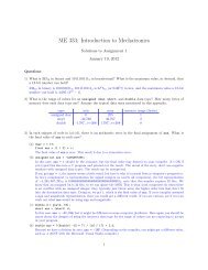
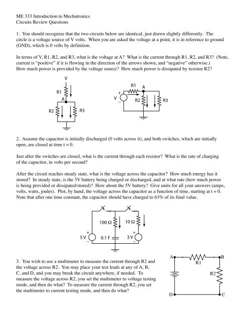
ME 333 Introduction to <strong>Mechatronics</strong><br />
Circuits Review Questions<br />
1. You should recognize that the two circuits below are identical, just drawn slightly differently. The<br />
circle is a voltage source of V volts. When you are asked the voltage at a point, it is in reference to ground<br />
(GND), which is 0 volts by definition.<br />
In terms of V, R1, R2, and R3, what is the voltage at A What is the current through R1, R2, and R3 (Note,<br />
current is “positive” if it is flowing in the direction of the arrows shown, and “negative” otherwise.)<br />
How much power is provided by the voltage source How much power is dissipated by resistor R2<br />
R1<br />
A<br />
V<br />
+<br />
V _<br />
R1<br />
R2<br />
A<br />
R3<br />
R2<br />
R3<br />
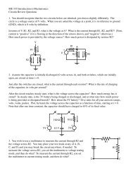
2. Assume the capacitor is initially discharged (0 volts across it), and both switches, which are initially<br />
open, are closed at time t = 0.<br />
Just after the switches are closed, what is the current through each resistor What is the rate of charging<br />
of the capacitor, in volts per second<br />
After the circuit reaches steady state, what is the voltage across the capacitor How much energy has it<br />
stored In steady state, is the 3V battery being charged or discharged, and at what rate (how much power<br />
is being provided or dissipated/stored) How about the 5V battery Give units for all your answers (amps,<br />
volts, watts, joules). Plot, by hand, the voltage across the capacitor as a function of time, starting at t = 0.<br />
Note that after one time constant, the capacitor should have charged to 63% of its final value.<br />
100 Ω<br />
10 Ω<br />
+<br />
+<br />
5 V<br />
_ 0.1 F 3 V<br />
_<br />
3. You wish to use a multimeter to measure the current through R2 and<br />
the voltage across R2. You may place your test leads at any of A, B,<br />
C, and D, and you may break the circuit anywhere, if needed. To<br />
measure the voltage across R2, you set the multimeter to voltage testing<br />
mode, and then do what To measure the current through R2, you set<br />
the multimeter to current testing mode, and then do what<br />
A<br />
D<br />
R1<br />
R2<br />
B<br />
C
4. Approximately plot the current through the diode as a function of the voltage across the diode.<br />
I<br />
I<br />
+ _<br />
Voltage<br />
-3V -2V -1V 1V 2V 3V<br />
I<br />
A 2<br />
5. The switch in the circuit at right has been closed for a<br />
long time, so that the circuit is in steady state. In all of your<br />
answers, make sure that the sign of the current is<br />
2H<br />
correct. All of your answers should be numbers with +<br />
I<br />
proper units. Assume that the forward bias voltage<br />
1<br />
of the diode is 0.7 V.<br />
10 V<br />
_<br />
a. Give the steady-state current I 1 .<br />
b. Give the steady-state current I 2 .<br />
50Ω<br />
c. What is the energy in the inductor<br />
d. The switch is now opened at t=0. What is I 1 the<br />
instant after the switch is opened<br />
e. At the instant after the switch is opened, what is I 2 <br />
f. At the instant after the switch is opened, give the<br />
voltage at point A (referenced to ground).<br />
g. At the instant after the switch is opened, give the rate of change of I 1 (that is, dI 1 /dt).<br />
h. Plot the voltage across, and current through, the inductor as a function of time from t=0. The plots should<br />
clearly show the time constant.<br />
6. For the transistor below, the voltage from the base to the emitter is V BE when the transistor is on, and<br />
when the transistor is saturated, the voltage from the collector to the emitter is V CEsat . In the linear (active)<br />
mode, the transistor satisfies I C = β I B , where β is the transistor gain. Give the ranges of V in voltages for<br />
which the transistor is off and for which it is saturated.<br />
V s<br />
V in<br />
R 1<br />
R 2
7. If this transistor is in saturation, what is a lower bound on its gain β<br />
(Remember I C = β I B when the transistor is in active mode.) Assume that the<br />
voltage from the collector to emitter is V CEsat = 0.2 V in saturation, and the<br />
voltage from the base to the emitter is V BE = 0.7 V when the transistor is on.<br />
These are common approximations we will make in this class.<br />
V in<br />
V s<br />
R 1<br />
R 2<br />
8. Consider the circuit at right. The transistor gain is β, the base-emitter voltage<br />
when the transistor is on is V BE<br />
, the collector-emitter voltage when the transistor<br />
is saturated is V CEsat<br />
, and the forward bias voltage of the diode is V D<br />
. All<br />
answers for this problem should be in terms only of some subset of these four<br />
values, V, and the resistances and inductance indicated at right.<br />
V<br />
+<br />
L<br />
_<br />
a. For what voltages of V in<br />
is the transistor saturated in steady state (i.e., the<br />
current through the inductor is not changing)<br />
b. Assume that the transistor has been saturated for long time, and then V in<br />
is<br />
suddenly set to zero. Clearly indicate on the circuit diagram the full current<br />
path after this switch.<br />
V in<br />
R 1<br />
R 2<br />
c. In the instant after V in<br />
is set to zero, what is the current through the inductor<br />
d. In the instant after V in<br />
is set to zero, what is the voltage across the inductor<br />
Is the voltage positive or negative, according to the sign convention in the diagram<br />
(positive voltage means that the voltage is higher at the “top” of the inductor)<br />
10 V<br />
9. Calculate the voltage range for V in<br />
for which the LED is off and for<br />
which the LED is at its maximum brightness in the circuit at right.<br />
The transistor gain is 100. Assume the diode drop and V BE<br />
when the<br />
transistor is on is 0.7 V and V CEsat<br />
is 0.2 V.<br />
V in<br />
10. Plot the output voltage for the circuit below if the<br />
input voltage is a sine wave from -5 V to 5 V.<br />
1000 Ω<br />
1000 Ω<br />
100 Ω<br />
V in<br />
V out
11. You can build a simple 3-bit digital-to-analog converter (DAC)<br />
using an op-amp as shown at right. The input voltages take values<br />
of either 0 or 1 V and represent a 3-bit binary number. At the output<br />
you want an analog representation of the 3-bit number,<br />
V out<br />
= -4V 2<br />
- 2V 1<br />
- V 0<br />
. What resistances R 0<br />
, R 1<br />
, and R 2<br />
should<br />
you use (Note: real DACs are not made this way.)<br />
V 1<br />
V 2<br />
R 0<br />
R 1<br />
R 2<br />
R<br />
_<br />
V out<br />
+<br />
<strong>12</strong>. In the circuit below, give V out<br />
as a function of V 1<br />
, V 2<br />
, R 1<br />
, R 2<br />
, R 3<br />
, and C (or some subset of these).<br />
V 0<br />
+<br />
R 2<br />
R 1<br />
V 1<br />
_<br />
V 2<br />
V out<br />
C<br />
+<br />
R 3<br />
13. In the circuit at right, give V out .<br />
C<br />
R<br />
V 1<br />
V 2<br />
R<br />
_<br />
V out