practice problem set - Northwestern Mechatronics Wiki
practice problem set - Northwestern Mechatronics Wiki
practice problem set - Northwestern Mechatronics Wiki
- No tags were found...

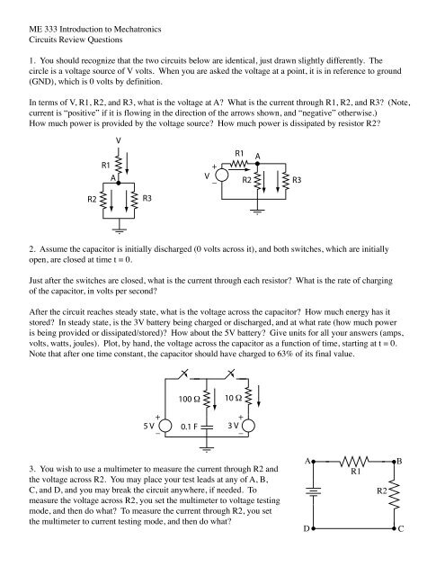
Create successful ePaper yourself
Turn your PDF publications into a flip-book with our unique Google optimized e-Paper software.
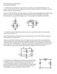
4. Approximately plot the current through the diode as a function of the voltage across the diode.II+ _Voltage-3V -2V -1V 1V 2V 3VIA 25. The switch in the circuit at right has been closed for along time, so that the circuit is in steady state. In all of youranswers, make sure that the sign of the current is2Hcorrect. All of your answers should be numbers with +Iproper units. Assume that the forward bias voltage1of the diode is 0.7 V.10 V_a. Give the steady-state current I 1 .b. Give the steady-state current I 2 .50Ωc. What is the energy in the inductor?d. The switch is now opened at t=0. What is I 1 theinstant after the switch is opened?e. At the instant after the switch is opened, what is I 2 ?f. At the instant after the switch is opened, give thevoltage at point A (referenced to ground).g. At the instant after the switch is opened, give the rate of change of I 1 (that is, dI 1 /dt).h. Plot the voltage across, and current through, the inductor as a function of time from t=0. The plots shouldclearly show the time constant.6. For the transistor below, the voltage from the base to the emitter is V BE when the transistor is on, andwhen the transistor is saturated, the voltage from the collector to the emitter is V CEsat . In the linear (active)mode, the transistor satisfies I C = β I B , where β is the transistor gain. Give the ranges of V in voltages forwhich the transistor is off and for which it is saturated.V sV inR 1R 2
7. If this transistor is in saturation, what is a lower bound on its gain β?(Remember I C = β I B when the transistor is in active mode.) Assume that thevoltage from the collector to emitter is V CEsat = 0.2 V in saturation, and thevoltage from the base to the emitter is V BE = 0.7 V when the transistor is on.These are common approximations we will make in this class.V inV sR 1R 28. Consider the circuit at right. The transistor gain is β, the base-emitter voltagewhen the transistor is on is V BE, the collector-emitter voltage when the transistoris saturated is V CEsat, and the forward bias voltage of the diode is V D. Allanswers for this <strong>problem</strong> should be in terms only of some sub<strong>set</strong> of these fourvalues, V, and the resistances and inductance indicated at right.V+L_a. For what voltages of V inis the transistor saturated in steady state (i.e., thecurrent through the inductor is not changing)?b. Assume that the transistor has been saturated for long time, and then V inissuddenly <strong>set</strong> to zero. Clearly indicate on the circuit diagram the full currentpath after this switch.V inR 1R 2c. In the instant after V inis <strong>set</strong> to zero, what is the current through the inductor?d. In the instant after V inis <strong>set</strong> to zero, what is the voltage across the inductor?Is the voltage positive or negative, according to the sign convention in the diagram(positive voltage means that the voltage is higher at the “top” of the inductor)?10 V9. Calculate the voltage range for V infor which the LED is off and forwhich the LED is at its maximum brightness in the circuit at right.The transistor gain is 100. Assume the diode drop and V BEwhen thetransistor is on is 0.7 V and V CEsatis 0.2 V. (Note: a betterapproximation for the LED drop is about 1.7 V.)V in10. Plot the output voltage for the circuit below if theinput voltage is a sine wave from -5 V to 5 V.1000 Ω1000 Ω100 ΩV inV out
11. You can build a simple 3-bit digital-to-analog converter (DAC)using an op-amp as shown at right. The input voltages take valuesof either 0 or 1 V and represent a 3-bit binary number. At the outputyou want an analog representation of the 3-bit number,V out= -4V 2- 2V 1- V 0. What resistances R 0, R 1, and R 2shouldyou use? (Note: real DACs are not made this way.)V 1V 2R 0R 1R 2R_V out+12. In the circuit below, give V outas a function of V 1, V 2, R 1, R 2, R 3, and C (or some sub<strong>set</strong> of these).V 0+R 2R 1V 1_V 2V outC+R 313. In the circuit at right, give V out .CRV 1V 2R_V out