WA-TX-03-R / WA-RX-03-R Operation Guide - Circuit Design, Inc.
WA-TX-03-R / WA-RX-03-R Operation Guide - Circuit Design, Inc.
WA-TX-03-R / WA-RX-03-R Operation Guide - Circuit Design, Inc.
- No tags were found...

Create successful ePaper yourself
Turn your PDF publications into a flip-book with our unique Google optimized e-Paper software.
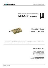
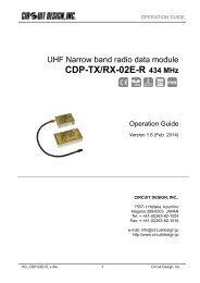
OPERATION GUIDE<br />
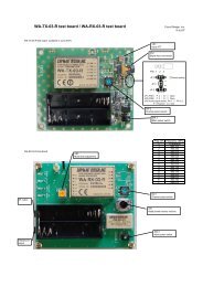
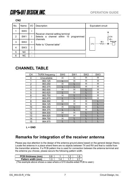
CN2<br />
No. Name I/O Description Equivalent circuit<br />
1 SW0 I<br />
2 SW1 I<br />
3 SW2 I<br />
4 SW3 I<br />
Receiver channel setting terminal<br />
Selects a channel within 15 programmed<br />
channels<br />
Refer to “Channel table”<br />
5 NC -<br />
6 NC -<br />
CHANNEL TABLE<br />
CH <strong>TX</strong>/<strong>RX</strong> frequency SW0 SW1 SW2 SW3<br />
0 Unavailable H H H H<br />
1 863.125 L H H H<br />
2 863.250 H L H H<br />
3 863.375 L L H H<br />
4 863.500 H H L H<br />
5 863.625 L H L H<br />
6 863.750 H L L H<br />
7 863.875 L L L H<br />
8 864.000 H H H L<br />
9 864.125 L H H L<br />
10 864.250 H L H L<br />
11 864.375 L L H L<br />
12 864.500 H H L L<br />
13 864.625 L H L L<br />
14 864.750 H L L L<br />
15 864.875 L L L L<br />
L = GND<br />
Remarks for integration of the receiver antenna<br />
Please pay due attention to the design of the antenna ground plane based on the general design theory.<br />
Locate the antenna in a place where there are no objects between <strong>TX</strong> and <strong>RX</strong> and that is visible from<br />
the transmitter antenna. If a PCB pattern line is used for connection between the antenna terminal and<br />
the antenna you choose, please secure the following pattern width.<br />
PCB thickness (mm) 0.8 1 1.2 1.6<br />
Pattern width (mm) 1.3 1.4 1.7 2.7<br />
(The example above shows a case where a G10 double-sided PCB is used.)<br />
OG_<strong>WA</strong>-<strong>03</strong>-R_V15e <strong>Circuit</strong> <strong>Design</strong>, <strong>Inc</strong>. 7