ADC 10-bit 2 Gsps Evaluation Board - TSEV83102G0B User Guide
ADC 10-bit 2 Gsps Evaluation Board - TSEV83102G0B User Guide
ADC 10-bit 2 Gsps Evaluation Board - TSEV83102G0B User Guide

Create successful ePaper yourself
Turn your PDF publications into a flip-book with our unique Google optimized e-Paper software.
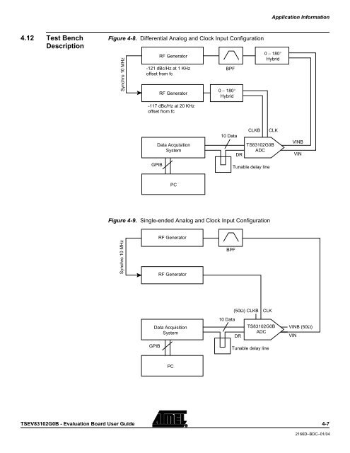
4.12 Test Bench<br />
Description<br />
Figure 4-8. Differential Analog and Clock Input Configuration<br />
Synchro <strong>10</strong> MHz<br />
Figure 4-9. Single-ended Analog and Clock Input Configuration<br />
Synchro <strong>10</strong> MHz<br />
RF Generator<br />
-121 dBc/Hz at 1 KHz<br />
offset from fc<br />
RF Generator<br />
-117 dBc/Hz at 20 KHz<br />
offset from fc<br />
GPIB<br />
Data Acquisition<br />
System<br />
PC<br />
Data Acquisition<br />
System<br />
GPIB<br />
RF Generator<br />
RF Generator<br />
PC<br />
0 − 180°<br />
Hybrid<br />
Application Information<br />
0 − 180°<br />
Hybrid<br />
TSEV83<strong>10</strong>2G0B - <strong>Evaluation</strong> <strong>Board</strong> <strong>User</strong> <strong>Guide</strong> 4-7<br />
BPF<br />
<strong>10</strong> Data<br />
BPF<br />
<strong>10</strong> Data<br />
DR<br />
CLKB CLK<br />
TS83<strong>10</strong>2G0B<br />
<strong>ADC</strong><br />
Tunable delay line<br />
(50Ω) CLKB CLK<br />
DR<br />
TS83<strong>10</strong>2G0B<br />
<strong>ADC</strong><br />
Tunable delay line<br />
VINB<br />
VIN<br />
VINB (50Ω)<br />
VIN<br />
2166D–BDC–01/04