

Mobile LPDDR2-PCM - Micron
Mobile LPDDR2-PCM - Micron
Mobile LPDDR2-PCM - Micron

Create successful ePaper yourself
Turn your PDF publications into a flip-book with our unique Google optimized e-Paper software.
Product Brief<br />
<strong>LPDDR2</strong>-<strong>PCM</strong> and <strong>Mobile</strong> <strong>LPDDR2</strong><br />
121-Ball MCP<br />
MT66R7072A10AB5ZZW.ZCA, MT66R7072A10ACUXZW.ZCA<br />
Features<br />
• <strong>Micron</strong> ® <strong>LPDDR2</strong>-<strong>PCM</strong> and <strong>LPDDR2</strong> components<br />
• RoHS-compliant, “green” package<br />
• Shared <strong>LPDDR2</strong>-<strong>PCM</strong> and <strong>LPDDR2</strong> interfaces<br />
• Space-saving multichip package<br />
• Ultra low-voltage core and I/O power supplies<br />
– V DD1 = 1.7–1.95V<br />
– V DDCA/V DDQ = 1.14–1.3V<br />
– V DD2 = 1.14–1.3V<br />
• Wireless temperature range: –25°C to +85°C<br />
<strong>LPDDR2</strong>-<strong>PCM</strong> Specific Features<br />
• Memory interface<br />
– 16-bit data bus width<br />
– Two data transfers per clock cycle<br />
– Clock frequency up to 400 MHz<br />
– Active to read/write delay: t RCD = 86ns<br />
– Configurable output drive strength<br />
• Memory architecture<br />
– 4-row data buffers (RDB)<br />
– Row data buffer size: 32B<br />
– 4-row address buffers (RAB)<br />
– Emulated block size: 128KB<br />
• Program/erase performance<br />
– Legacy programming mode up to 10MB/s (TYP)<br />
– Overwrite up to 3 MB/s (TYP)<br />
– Legacy block erase time: 60ms (TYP)<br />
• Dual operations<br />
– PROGRAM/ERASE in one partition while READ<br />
in other partitions<br />
– No delay between READ and WRITE operations<br />
• Locking scheme<br />
– All blocks locked at power-up<br />
– 8Mb lock region<br />
– Any combination of regions can be locked<br />
– Absolute write protection with<br />
V ACC = V SS<br />
• Quality and reliability<br />
– Minimum 100,000 WRITE<br />
cycles per row<br />
Product Brief – 121-Ball <strong>LPDDR2</strong>-<strong>PCM</strong> and <strong>LPDDR2</strong> MCP<br />
Features<br />
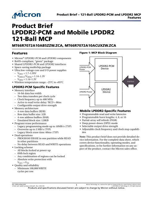
Figure 1: MCP Block Diagram<br />
<strong>LPDDR2</strong>-<strong>PCM</strong><br />
Power<br />
<strong>LPDDR2</strong> Power<br />
<strong>LPDDR2</strong>-<strong>PCM</strong><br />
Device<br />
<strong>LPDDR2</strong><br />
Device<br />
<strong>LPDDR2</strong><br />
Interface<br />
<strong>Mobile</strong> <strong>LPDDR2</strong>-Specific Features<br />
• Programmable read and write latencies<br />
• Programmable burst lengths: 4, 8, or 16<br />
• Partial-array self refresh (PASR)<br />
• Deep power-down (DPD) mode<br />
• Selectable output drive strength<br />
• Adjustable clock frequency and clock stop capabilities<br />
Note: This product brief does not provide detailed device<br />
information. For the complete data sheet, which<br />
covers device functionality, operating modes, and<br />
specifications, or for further information on any aspect<br />
of the product, contact the <strong>Micron</strong> sales office.<br />
PDF: 09005aef84e25954<br />
121ball_pcm_lpddr2_product_brief.pdf – Rev. A 8/12 EN 1 <strong>Micron</strong> Technology, Inc. reserves the right to change products or specifications without notice.<br />
© 2012 <strong>Micron</strong> Technology, Inc. All rights reserved.<br />
Products and specifications discussed herein are subject to change by <strong>Micron</strong> without notice.
Part Numbering Information<br />
<strong>Micron</strong> <strong>LPDDR2</strong>-<strong>PCM</strong> and <strong>LPDDR2</strong> devices are available in different configurations and densities. The MCP/PoP<br />
part numbering guide is available at www.micron.com/numbering.<br />
Figure 2: Part Number Chart<br />
<strong>Micron</strong> Technology<br />
Product Family<br />
66R = <strong>LPDDR2</strong>-<strong>PCM</strong> I/F + <strong>LPDDR2</strong><br />
Density<br />
<strong>PCM</strong> xNAND x<strong>LPDDR2</strong><br />
0 N/A<br />
1 32Mb = 4MB 16Mb = 2MB<br />
2 64Mb = 8MB 32Mb = 4MB<br />
3 128Mb = 16MB 64Mb = 8MB<br />
4 256Mb = 32MB 128Mb = 16MB<br />
5 512Mb = 64MB 256Mb = 32MB<br />
6 768Mb = 96MB 384Mb = 48MB<br />
7 1Gb = 128MB 512Mb = 64MB<br />
Voltage Range (Core_ I/0)<br />
<strong>PCM</strong> <strong>LPDDR2</strong><br />
1 1.8_1.8 1.8_1.8<br />
2 1.8_1.2 1.8_1.2<br />
Die Count<br />
<strong>PCM</strong> <strong>LPDDR2</strong><br />
A 1 1<br />
B 1 2<br />
<strong>PCM</strong> Configuration<br />
Bus Width Frequency<br />
1 x16 166 MHz<br />
2 x16 266 MHz<br />
3 x16 333 MHz<br />
4 x16 400 MHz<br />
Device Marking<br />
Product Brief – 121-Ball <strong>LPDDR2</strong>-<strong>PCM</strong> and <strong>LPDDR2</strong> MCP<br />
Features<br />
MT 66R 707 2 A 1 0 A CUX* Z W . ZCA - ES<br />
Production Status<br />
Blank = Production<br />
ES = Engineering samples<br />
MS = Mechanical samples<br />
Die Revision<br />
Contact factory<br />
Operating Temperature Range<br />
W = –25°C to +85°C (Wireless)<br />
I = –40°C to +85°C (Industrial)<br />
Special Options<br />
Contact factory<br />
Package Codes<br />
B5Z = 121-ball WFBGA, 11mmx10mmx0.8mm<br />
CUX = 121-ball WFBGA, 8mmx8mmx0.8mm<br />
*X = a null character used as a placeholder<br />
<strong>LPDDR2</strong> Description<br />
0 = N/A<br />
A = X16DDR2_S4 2KB Page<br />
B = X16DDR2_S2 2KB Page<br />
NAND Description<br />
Due to the size of the package, the <strong>Micron</strong>-standard part number is not printed on the top of the device. Instead,<br />
an abbreviated device mark consisting of a 5-digit alphanumeric code is used. The abbreviated device marks are<br />
cross-referenced to the <strong>Micron</strong> part numbers at the FBGA Part Marking Decoder site: www.micron.com/decoder.<br />
To view the location of the abbreviated mark on the device, refer to customer service note CSN-11, “Product Mark/<br />
Label,” at www.micron.com/csn.<br />
PDF: 09005aef84e25954<br />
121ball_pcm_lpddr2_product_brief.pdf – Rev. A 8/12 EN 2 <strong>Micron</strong> Technology, Inc. reserves the right to change products or specifications without notice.<br />
© 2012 <strong>Micron</strong> Technology, Inc. All rights reserved.<br />
0 = N/A
MCP General Description<br />
Device Diagrams<br />
<strong>Micron</strong> MCP products combine <strong>LPDDR2</strong>-<strong>PCM</strong> and <strong>Mobile</strong> <strong>LPDDR2</strong> devices in a single<br />
MCP. These products target mobile applications with low-power, high-performance,<br />
and minimal package-footprint design requirements. The <strong>LPDDR2</strong>-<strong>PCM</strong> and <strong>Mobile</strong><br />
<strong>LPDDR2</strong> devices are also members of the <strong>Micron</strong> discrete memory products portfolio.<br />
The bus architecture of this device also supports separate <strong>LPDDR2</strong>-<strong>PCM</strong> and <strong>Mobile</strong><br />
<strong>LPDDR2</strong> functionality without concern for device interaction.<br />
Figure 3: 121-Ball (<strong>LPDDR2</strong>-<strong>PCM</strong> and <strong>LPDDR2</strong>) Functional Block Diagram<br />
V DD1<br />
V DDQ<br />
V DDCA<br />
V SS<br />
V SSQ<br />
V SSCA<br />
V REFDQ<br />
V REFCA<br />
V DD2<br />
Product Brief – 121-Ball <strong>LPDDR2</strong>-<strong>PCM</strong> and <strong>LPDDR2</strong> MCP<br />
MCP General Description<br />
<strong>LPDDR2</strong>–<strong>PCM</strong><br />
<strong>LPDDR2</strong><br />
NV-CS#<br />
NV-CKE<br />
D-CS#<br />
D-CKE<br />
CK/CK#<br />
DQS[1:0]<br />
DQS#[1:0]<br />
DQ[15:0]<br />
DM[1:0]<br />
CA[9:0]<br />
PDF: 09005aef84e25954<br />
121ball_pcm_lpddr2_product_brief.pdf – Rev. A 8/12 EN 3 <strong>Micron</strong> Technology, Inc. reserves the right to change products or specifications without notice.<br />
© 2012 <strong>Micron</strong> Technology, Inc. All rights reserved.<br />
ZQ
Ball Assignments and Descriptions<br />
Figure 4: 121-Ball VFBGA (<strong>LPDDR2</strong>-<strong>PCM</strong> x16; <strong>LPDDR2</strong> x16) Ball Assignments<br />
A<br />
B<br />
C<br />
D<br />
E<br />
F<br />
G<br />
H<br />
J<br />
K<br />
L<br />
M<br />
N<br />
P<br />
R<br />
1 2 3 4 5 6 7 8 9 10 11<br />
DNU<br />
DNU<br />
NC<br />
V DD2<br />
V SS<br />
V DD1<br />
V SSCA<br />
V DDCA<br />
V DD2<br />
CK<br />
NV-CS0#<br />
CA4<br />
V DDCA<br />
DNU<br />
DNU<br />
DNU<br />
NC<br />
NC<br />
NC<br />
ZQ<br />
CA8<br />
CA7<br />
CA5<br />
V REF(CA)<br />
CK#<br />
D-CS#<br />
CA3<br />
CA2<br />
V SSCA<br />
DNU<br />
NC<br />
NC<br />
NC<br />
CA9<br />
CA6<br />
V SS<br />
NC<br />
CA1<br />
CA0<br />
V SS<br />
Product Brief – 121-Ball <strong>LPDDR2</strong>-<strong>PCM</strong> and <strong>LPDDR2</strong> MCP<br />
Ball Assignments and Descriptions<br />
NC<br />
NC<br />
RFU<br />
V DD2<br />
NC<br />
NC<br />
NC<br />
NC<br />
NC<br />
NC<br />
NC<br />
NC<br />
NV-CKE0<br />
D-CKE<br />
V DD1<br />
NC<br />
NC<br />
NC<br />
NC<br />
NC<br />
NC<br />
NC<br />
NC<br />
RFU<br />
V ACC<br />
V SS<br />
1 2 3 4 5 6 7 8 9 10 11<br />
V DD2<br />
V DD1<br />
NC<br />
NC<br />
NC<br />
NC<br />
NC<br />
NC<br />
NC<br />
DQ0<br />
V DD2<br />
V SS<br />
DQ15<br />
DQ1<br />
V SS<br />
<strong>LPDDR2</strong>-specific<br />
V DDQ<br />
DQ14<br />
DQ11<br />
DQ8<br />
DQS1#<br />
DQS0#<br />
DQ7<br />
DQ3<br />
DQ4<br />
V DDQ<br />
DNU<br />
V SSQ<br />
DQ12<br />
DQ10<br />
DQ9<br />
DQS1<br />
DM1<br />
V REF(DQ)<br />
DM0<br />
DQS0<br />
DQ6<br />
DQ5<br />
DQ2<br />
V SSQ<br />
DNU<br />
DNU<br />
DNU<br />
DQ13<br />
V SSQ<br />
V DDQ<br />
V SSQ<br />
V DDQ<br />
V DD2<br />
V DD1<br />
V DDQ<br />
V SSQ<br />
V DDQ<br />
V SSQ<br />
DNU<br />
DNU<br />
LPDDR-<strong>PCM</strong>-specific<br />
PDF: 09005aef84e25954<br />
121ball_pcm_lpddr2_product_brief.pdf – Rev. A 8/12 EN 4 <strong>Micron</strong> Technology, Inc. reserves the right to change products or specifications without notice.<br />
© 2012 <strong>Micron</strong> Technology, Inc. All rights reserved.<br />
A<br />
B<br />
C<br />
D<br />
E<br />
F<br />
G<br />
H<br />
J<br />
K<br />
L<br />
M<br />
N<br />
P<br />
R
Table 1: x16 <strong>LPDDR2</strong>-<strong>PCM</strong> Ball Descriptions<br />
Symbol Type Description<br />
NV-CS# Input Chip select: CS# is considered part of the command code and is sampled at the<br />
rising edge of CK. When registered, CS# LOW enables, and CS# HIGH disables,<br />
the command decoder. All commands are masked when CS# is registered HIGH.<br />
NV-CKE Input Clock enable: CKE HIGH activates and CKE LOW deactivates the internal clock<br />
signals, input buffers, and output drivers. Power-saving modes are entered and<br />
exited via CKE transitions. CKE is considered part of the command code. CKE is<br />
sampled at the rising edge of CK.<br />
Table 2: x16 <strong>Mobile</strong> <strong>LPDDR2</strong> Ball Descriptions<br />
Product Brief – 121-Ball <strong>LPDDR2</strong>-<strong>PCM</strong> and <strong>LPDDR2</strong> MCP<br />
Ball Assignments and Descriptions<br />
Symbol Type Description<br />
D-CKE Input Clock enable.<br />
D-CKE is used for a single <strong>LPDDR2</strong>. For the signal description, refer to NV-CKE<br />
description.<br />
D-CS# Input Chip select:<br />
D-CS# is used for a single <strong>LPDDR2</strong>. For the signal description, refer to NV-CS# description.<br />
PDF: 09005aef84e25954<br />
121ball_pcm_lpddr2_product_brief.pdf – Rev. A 8/12 EN 5 <strong>Micron</strong> Technology, Inc. reserves the right to change products or specifications without notice.<br />
© 2012 <strong>Micron</strong> Technology, Inc. All rights reserved.
Table 3: <strong>LPDDR2</strong> Ball Descriptions<br />
Symbol Type Description<br />
CA[9:0] Input Command/address inputs: Provide the command and address inputs according to<br />
the command truth table.<br />
CK, CK# Input Clock: CK and CK# are differential clock inputs. All CA inputs are sampled on<br />
both the positive and negative edge of CK. CS and CKE inputs are sampled at<br />
the positive edge of CK. AC timings are referenced to clock.<br />
DM[1:0] Input Data mask:DM is an input mask signal for write data. Although DM balls are input-only,<br />
the DM loading is designed to match that of DQ and DQS balls.<br />
DM[1:0] is DM for each of the two data bytes, respectively.<br />
DQ[15:0] Input/<br />
output<br />
DQS[3:0]<br />
DQS#[3:0]<br />
Input/<br />
output<br />
Data bus: Data inputs/outputs.<br />
Data strobe: Coordinates READ/WRITE transfers of data; one DQS/DQS# pair per<br />
DQ byte.<br />
V DD1 Supply V DD1: <strong>LPDDR2</strong> power supply 1.<br />
V DD2 Supply V DD2: <strong>LPDDR2</strong> power supply 2.<br />
V DDCA Supply V DDCA: <strong>LPDDR2</strong> CA power supply.<br />
V DDQ Supply V DDQ: <strong>LPDDR2</strong> I/O power supply.<br />
V REFCA Supply V REFCA: <strong>LPDDR2</strong> reference for CA pins.<br />
V REFDQ Supply V REFDQ: <strong>LPDDR2</strong> reference for DQ pins.<br />
V SSCA Supply V SSCA: <strong>LPDDR2</strong> I/O ground.<br />
V SSQ Supply V SSQ: <strong>LPDDR2</strong> I/O ground.<br />
V SS Supply V SS: Shared ground.<br />
ZQ Input External impedance (240-Ohm): This signal is used to calibrate the device output<br />
impedance.<br />
Table 4: Non-Device-Specific Descriptions<br />
Product Brief – 121-Ball <strong>LPDDR2</strong>-<strong>PCM</strong> and <strong>LPDDR2</strong> MCP<br />
Ball Assignments and Descriptions<br />
Symbol Type Description<br />
DNU – Do not use: Must be grounded or left floating.<br />
NC – No connect: Not internally connected.<br />
PDF: 09005aef84e25954<br />
121ball_pcm_lpddr2_product_brief.pdf – Rev. A 8/12 EN 6 <strong>Micron</strong> Technology, Inc. reserves the right to change products or specifications without notice.<br />
© 2012 <strong>Micron</strong> Technology, Inc. All rights reserved.
Phase Change Memory General Description<br />
Product Brief – 121-Ball <strong>LPDDR2</strong>-<strong>PCM</strong> and <strong>LPDDR2</strong> MCP<br />
Phase Change Memory General Description<br />
<strong>PCM</strong> is a new class of nonvolatile memory devices that stores information through a reversible<br />
structural phase change in a chalcogenide material. The material exhibits a<br />
change in both electrical and optical properties when changed from the amorphous<br />
(disordered) to the polycrystalline (regularly ordered) state. The amorphous state corresponds<br />
to the reset state (0); the polycrystalline state corresponds to the set state (1). In<br />
<strong>PCM</strong>, information is stored during the change in resistance the chalcogenide material<br />
undergoes during a phase change<br />
The device uses a DDR architecture on the command/address (CA) bus to reduce the<br />
number of input pins in the system. The 10-bit CA bus contains command, address, and<br />
row buffer information. Each command uses one clock cycle, during which command<br />
information is transferred on both the positive and negative edge of the clock. The device<br />
also uses a DDR architecture on the DQ pins to achieve high-speed operation.<br />
The <strong>LPDDR2</strong>-<strong>PCM</strong> device uses a complete set of commands that are compatible with<br />
the JEDEC industry-standard specification No. JESD209-2E.<br />
The DDR architecture is essentially a 4n-prefetch architecture with an interface designed<br />
to transfer two data bits per DQ every clock cycle at the I/O pins. A single read or<br />
write access effectively consists of a single, 4n-bit wide, one-clock-cycle data transfer at<br />
the internal core and four corresponding, n-bit wide, one-half-clock-cycle data transfers<br />
at the I/O pins.<br />
The device is organized into four RABs and RDBs, 32 bytes each. Read or write accesses<br />
to device are performed issuing a sequence of PREACTIVE commands to deliver part of<br />
the row address to one of four RABs in the device; ACTIVATE commands to fill one of<br />
the four RDBs in the device; and READ or WRITE commands.<br />
Operations other than array reads are performed by accessing an overlay window that is<br />
mapped over the array space of the memory. The overlay window base address is programmed<br />
using the mode registers.<br />
The device can be erased electrically at block level and programmed in-system on a<br />
word-by-word basis using a V DD1 supply for the circuitry and V DDQ supply for the I/O<br />
pins. An optional V ACC power supply is provided for factory programming.<br />
A multiple partition architecture allows dual operations: While writing or erasing in one<br />
partition, READ operations are possible in other partitions. Only one partition at a time<br />
can be in write or erase mode.<br />
Erase can be suspended to perform a WRITE or READ operation in any other block except<br />
for the one being erased, and then resumed. Writing can be suspended to read data<br />
at any memory location except the one being modified, and then resumed.<br />
To issue embedded commands like PROGRAM or ERASE, the operation code and data<br />
are written to the overlay window of the memory. An internal program/erase controller<br />
manages the timings necessary for embedded operations. The end of a WRITE or<br />
ERASE operation can be detected and any error conditions identified in the status register.<br />
The command set required to control the memory is consistent with the JEDEC<br />
standard.<br />
Read and write accesses to the device are burst oriented at different frequencies using a<br />
differential clock up to 400 MHz. Accesses start at a selected location and continue for a<br />
configured number of locations.<br />
PDF: 09005aef84e25954<br />
121ball_pcm_lpddr2_product_brief.pdf – Rev. A 8/12 EN 7 <strong>Micron</strong> Technology, Inc. reserves the right to change products or specifications without notice.<br />
© 2012 <strong>Micron</strong> Technology, Inc. All rights reserved.
Product Brief – 121-Ball <strong>LPDDR2</strong>-<strong>PCM</strong> and <strong>LPDDR2</strong> MCP<br />
Phase Change Memory General Description<br />
The device features a power-down mode. When clock enable (CKE) is registered LOW,<br />
power-down mode is enabled. In this condition, the power consumption is reduced to<br />
the standby value.<br />
The device features an individual locking region scheme that allows any region to be<br />
locked or unlocked, enabling code and data protection. The array is divided into 8Mb<br />
locking regions. All locking regions have three levels of protection. They can be locked<br />
and locked down individually, preventing any accidental writing or erasure. There is also<br />
additional hardware protection against writing and erasing. When V ACC < V ACCLK, all<br />
lock regions are protected against program or erase. All lock regions are locked at power-up.<br />
V ACC shall not change during the period starting from at least 1µs prior to the initiation<br />
of any embedded operation until that embedded operation is complete.<br />
The device includes a 64-bit segment area, containing a unique 64-bit device number<br />
and a 256-bit (16-word) protection register area that is one-time programmable (OTP)<br />
by the user. The user-programmable region can be permanently protected, programming<br />
the 16-bit protection register lock. See Security Features and Protection Registers<br />
for more details.<br />
<strong>PCM</strong> offers bit alterability or an overwrite feature: <strong>PCM</strong> technology supports the ability<br />
to change each memory bit independently from 0 to 1 or 1 to 0 without erasing the<br />
block first. Bit alterability enables software to write to the nonvolatile memory similar to<br />
writing to RAM or EEPROM without the overhead of erasing blocks prior to writing. Bitalterable<br />
writes use command sequences similar to word writes and buffer writes. This<br />
mode is often referred to as overwrite as opposed to program, in which only 0s are written<br />
and 1s are treated as masks.<br />
The device is rated at 100,000 write alterations per row. The device is supplied with all<br />
the bits erased (set to 1).<br />
PDF: 09005aef84e25954<br />
121ball_pcm_lpddr2_product_brief.pdf – Rev. A 8/12 EN 8 <strong>Micron</strong> Technology, Inc. reserves the right to change products or specifications without notice.<br />
© 2012 <strong>Micron</strong> Technology, Inc. All rights reserved.
<strong>LPDDR2</strong>-<strong>PCM</strong> Organization<br />
Array<br />
Memory Map<br />
Table 5: 512Mb <strong>LPDDR2</strong>-<strong>PCM</strong><br />
The 512Mb device has a 512-block array and is divided into 64Mb partitions. There are 8<br />
partitions containing 64 blocks of 128KB each.<br />
The 1Gb device has a 1024-block array and is divided into 64Mb partitions. There are 16<br />
partitions containing 64 blocks of 128KB each.<br />
Block<br />
Number Size (KB)<br />
Word Address<br />
Range<br />
Partition 7 64Mb 511 128 1FF0000–1FFFFFF<br />
⋮ ⋮ ⋮<br />
448 128 1C00000–1C0FFFF<br />
Partition 0 64Mb 63 128 03F0000–03FFFFF<br />
Table 6: 1Gb <strong>LPDDR2</strong>-<strong>PCM</strong><br />
Product Brief – 121-Ball <strong>LPDDR2</strong>-<strong>PCM</strong> and <strong>LPDDR2</strong> MCP<br />
<strong>LPDDR2</strong>-<strong>PCM</strong> Organization<br />
⋮ ⋮ ⋮<br />
0 128 0000000–000FFFF<br />
Block<br />
Number Size (KB)<br />
Word Address<br />
Range<br />
Partition 15 64Mb 1023 128 3FF0000–3FFFFFF<br />
⋮ ⋮ ⋮<br />
960 128 3C00000–3C0FFFF<br />
Partition 0 64Mb 63 128 03F0000–03FFFFF<br />
⋮ ⋮ ⋮<br />
0 128 0000000–000FFFF<br />
PDF: 09005aef84e25954<br />
121ball_pcm_lpddr2_product_brief.pdf – Rev. A 8/12 EN 9 <strong>Micron</strong> Technology, Inc. reserves the right to change products or specifications without notice.<br />
© 2012 <strong>Micron</strong> Technology, Inc. All rights reserved.
Package Dimensions<br />
Figure 5: 121-Ball VFBGA – 8mm x 8mm x 0.8mm (Package Code: CU)<br />
121X Ø0.32<br />
Dimensions<br />
apply to solder<br />
balls post-reflow<br />
on Ø0.30 SMD<br />
ball pads.<br />
8 ±0.1<br />
7 CTR<br />
0.5 TYP<br />
10<br />
11<br />
9<br />
8<br />
7<br />
6<br />
5<br />
0.5 TYP<br />
5 CTR<br />
8 ±0.1<br />
4<br />
Product Brief – 121-Ball <strong>LPDDR2</strong>-<strong>PCM</strong> and <strong>LPDDR2</strong> MCP<br />
Package Dimensions<br />
3<br />
Ball A1 ID<br />
(covered by SR)<br />
Note: 1. All dimensions are in millimeters.<br />
2<br />
1<br />
A<br />
B<br />
C<br />
D<br />
E<br />
F<br />
G<br />
H<br />
J<br />
K<br />
L<br />
M<br />
N<br />
P<br />
R<br />
A<br />
Seating plane<br />
0.08 A<br />
0.7 ±0.1<br />
0.16 MIN<br />
Ball A1 ID<br />
PDF: 09005aef84e25954<br />
121ball_pcm_lpddr2_product_brief.pdf – Rev. A 8/12 EN 10 <strong>Micron</strong> Technology, Inc. reserves the right to change products or specifications without notice.<br />
© 2012 <strong>Micron</strong> Technology, Inc. All rights reserved.
Figure 6: 121-Ball VFBGA – 11m x 10mm x 0.8mm (Package Code: B5Z)<br />
121X Ø0.3 ±0.05<br />
10 ±0.1<br />
7 CTR<br />
0.5 TYP<br />
10 8 6 4 2<br />
11 9 7 5 3 1<br />
0.5 TYP<br />
5 CTR<br />
11 ±0.1<br />
Product Brief – 121-Ball <strong>LPDDR2</strong>-<strong>PCM</strong> and <strong>LPDDR2</strong> MCP<br />
Package Dimensions<br />
Ball A1 ID<br />
A<br />
B C<br />
D<br />
E<br />
F G<br />
H J<br />
K<br />
L<br />
M<br />
N<br />
P<br />
R<br />
Note: 1. All dimensions are in millimeters.<br />
A<br />
Seating plane<br />
0.08 A<br />
0.8 MAX<br />
0.15 MIN<br />
Ball A1 ID<br />
PDF: 09005aef84e25954<br />
121ball_pcm_lpddr2_product_brief.pdf – Rev. A 8/12 EN 11 <strong>Micron</strong> Technology, Inc. reserves the right to change products or specifications without notice.<br />
© 2012 <strong>Micron</strong> Technology, Inc. All rights reserved.
Revision History<br />
Rev. A – 08/12<br />
• Initial release<br />
Product Brief – 121-Ball <strong>LPDDR2</strong>-<strong>PCM</strong> and <strong>LPDDR2</strong> MCP<br />
Revision History<br />
8000 S. Federal Way, P.O. Box 6, Boise, ID 83707-0006, Tel: 208-368-3900<br />
www.micron.com/productsupport Customer Comment Line: 800-932-4992<br />
<strong>Micron</strong> and the <strong>Micron</strong> logo are trademarks of <strong>Micron</strong> Technology, Inc.<br />
All other trademarks are the property of their respective owners.<br />
This data sheet contains minimum and maximum limits specified over the power supply and temperature range set forth herein.<br />
Although considered final, these specifications are subject to change, as further product development and data characterization sometimes<br />
occur.<br />
PDF: 09005aef84e25954<br />
121ball_pcm_lpddr2_product_brief.pdf – Rev. A 8/12 EN 12 <strong>Micron</strong> Technology, Inc. reserves the right to change products or specifications without notice.<br />
© 2012 <strong>Micron</strong> Technology, Inc. All rights reserved.


