

Mobile LPDDR2-PCM - Micron
Mobile LPDDR2-PCM - Micron
Mobile LPDDR2-PCM - Micron

Create successful ePaper yourself
Turn your PDF publications into a flip-book with our unique Google optimized e-Paper software.
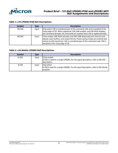
Table 1: x16 <strong>LPDDR2</strong>-<strong>PCM</strong> Ball Descriptions<br />
Symbol Type Description<br />
NV-CS# Input Chip select: CS# is considered part of the command code and is sampled at the<br />
rising edge of CK. When registered, CS# LOW enables, and CS# HIGH disables,<br />
the command decoder. All commands are masked when CS# is registered HIGH.<br />
NV-CKE Input Clock enable: CKE HIGH activates and CKE LOW deactivates the internal clock<br />
signals, input buffers, and output drivers. Power-saving modes are entered and<br />
exited via CKE transitions. CKE is considered part of the command code. CKE is<br />
sampled at the rising edge of CK.<br />
Table 2: x16 <strong>Mobile</strong> <strong>LPDDR2</strong> Ball Descriptions<br />
Product Brief – 121-Ball <strong>LPDDR2</strong>-<strong>PCM</strong> and <strong>LPDDR2</strong> MCP<br />
Ball Assignments and Descriptions<br />
Symbol Type Description<br />
D-CKE Input Clock enable.<br />
D-CKE is used for a single <strong>LPDDR2</strong>. For the signal description, refer to NV-CKE<br />
description.<br />
D-CS# Input Chip select:<br />
D-CS# is used for a single <strong>LPDDR2</strong>. For the signal description, refer to NV-CS# description.<br />
PDF: 09005aef84e25954<br />
121ball_pcm_lpddr2_product_brief.pdf – Rev. A 8/12 EN 5 <strong>Micron</strong> Technology, Inc. reserves the right to change products or specifications without notice.<br />
© 2012 <strong>Micron</strong> Technology, Inc. All rights reserved.


