

Technical Note - Micron
Technical Note - Micron
Technical Note - Micron

You also want an ePaper? Increase the reach of your titles
YUMPU automatically turns print PDFs into web optimized ePapers that Google loves.
TN-47-21: FBDIMM – Channel Utilization (Bandwidth and Power)<br />
Introduction<br />
<strong>Technical</strong> <strong>Note</strong><br />
FBDIMM – Channel Utilization (Bandwidth and Power)<br />
Introduction<br />
Memory architectures are shifting from stub bus technology to high-speed linking. The<br />
traditional stub bus works well for slower devices, but has several limitations when<br />
supporting the higher bandwidth signals required in memory systems today. For<br />
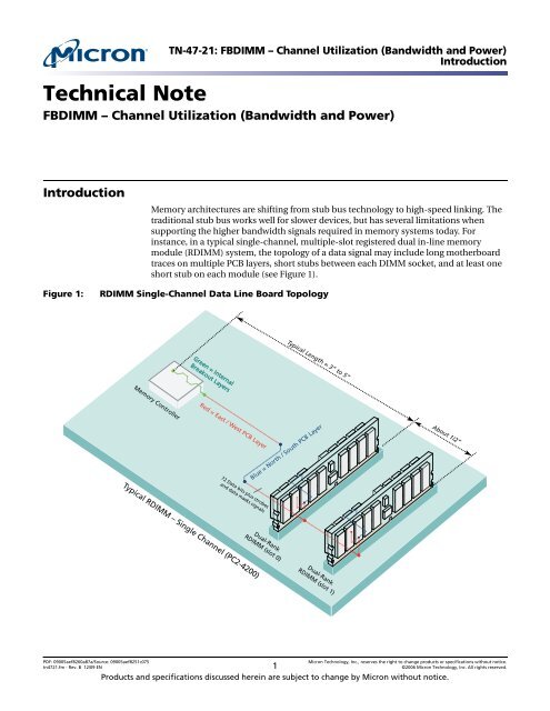
instance, in a typical single-channel, multiple-slot registered dual in-line memory<br />
module (RDIMM) system, the topology of a data signal may include long motherboard<br />
traces on multiple PCB layers, short stubs between each DIMM socket, and at least one<br />
short stub on each module (see Figure 1).<br />
Figure 1: RDIMM Single-Channel Data Line Board Topology<br />
Memory Controller<br />
Green Green = = Internal Internal<br />
Breakout Breakout Layers Layers<br />
Red = East / West PCB Layer<br />
72 Data bits plus strobes<br />
and data masks signals<br />
Typical RDIMM – Single Channel (PC2-4200)<br />
Blue = North / South PCB Layer<br />
Dual-Rank<br />
RDIMM (slot 0)<br />
Typical Length = 3” to 5”<br />
Dual-Rank<br />
RDIMM (slot 1)<br />
About 1/2”<br />
PDF: 09005aef8260a87a/Source: 09005aef8251c075 <strong>Micron</strong> Technology, Inc., reserves the right to change products or specifications without notice.<br />
tn4721.fm - Rev. B 12/09 EN 1 ©2006 <strong>Micron</strong> Technology, Inc. All rights reserved.<br />
Products and specifications discussed herein are subject to change by <strong>Micron</strong> without notice.
TN-47-21: FBDIMM – Channel Utilization (Bandwidth and Power)<br />
Introduction<br />
As the signal propagates from the memory controller through the connector and<br />
expands out to the DRAM, several of the traces can be mismatched. At slower clock rates<br />
this may not make a difference, but at higher signal rates, these signal mismatches can<br />
degrade signal quality. Other issues that can compromise RDIMM performance are:<br />
• Signal integrity problems due to unbalanced signal loads from a mixture of different<br />
module configurations<br />
Limitations of bandwidth due to possible bus collisions<br />
Bus contention can be characterized in a typical RDIMM system or directly from the<br />
DDR2 component data sheet. For example, in most RDIMM single-channel systems<br />
there is only one copy of data signals. This means all DRAM in any given bytelane will<br />
share a single board-level trace for their combined DQS signals. For the memory<br />
controller to query data from different slots or module ranks, it must ensure that there is<br />
not bus contention on the strobe lines. To do this, the controller must insert at least one<br />
dead clock cycle between sequential READ commands of the independent ranks.<br />
Furthermore, in a single-channel RDIMM system, it is impossible to simultaneously<br />
write data to any one rank while reading data from any other rank (regardless of how<br />
many RDIMMs are in the channel).<br />
RDIMM systems have proven to be a stable and an excellent solution for multiple<br />
memory technologies. PC2-4200 RDIMM systems, which run with a data transfer rate of<br />
533 MT/s per bit, can typically only support two dual-rank (DR) RDIMMs per memory<br />
channel. This is due to the stub bus architecture and the reflections this architecture<br />
causes. If more than two DR PC2-4200 (or faster) modules are required, the system may<br />
need to support a dual-channel design. This is a very limiting factor for systems that<br />
require extremely high memory density. This is because a dual-channel design duplicates<br />
all address, command, control, and data signals from the memory controller by<br />
routing them in parallel with the first channel. In some cases, a dual-channel design also<br />
requires a second memory controller and a large amount of board routing space.<br />
Fully buffered DIMM (FBDIMM) systems offer virtually unlimited scalability of density,<br />
a significantly reduced number of routed motherboard signals, and high bandwidth<br />
solutions, all with an extremely reliable channel protocol. FBDIMM systems use DDR2<br />
memory, but have a topology that uses a high-speed point-to-point interface between<br />
the controller and the first DIMM and between each other DIMM. The on-module interface<br />
between the advanced memory buffer (AMB) and the DDR2 DRAM completely<br />
isolates the DRAM from the high-speed channel and supports a point-to-two-point<br />
memory interface (see Figure 2). This new FBDIMM architecture also supports simultaneous<br />
READ and WRITE cycles within a single memory channel but on different DIMMs.<br />
For a comparison of a typical RDIMM channel to a typical FBDIMM channel, see<br />
Figure 3.<br />
This technical note provides an introduction to the high-speed link, explains what to<br />
expect in regard to channel bandwidth, and outlines how to optimize performance,<br />
including some power analysis techniques.<br />
PDF: 09005aef8260a87a/Source: 09005aef8251c075 <strong>Micron</strong> Technology, Inc., reserves the right to change products or specifications without notice.<br />
tn4721.fm - Rev. B 12/09 EN 2 ©2006 <strong>Micron</strong> Technology, Inc. All rights reserved.
Figure 2: FBDIMM Single-Channel Board Topology<br />
Routing of one southbound bit<br />
Memory<br />
Controller<br />
Dual-Rank<br />
FBIMM (slot 0)<br />
TN-47-21: FBDIMM – Channel Utilization (Bandwidth and Power)<br />
Introduction<br />
Routing between each FBDIMM is point-to-point<br />
Typical FBDIMM - Single Channel (8 GB/s)<br />
Dual-Rank<br />
FBIMM (slot 7)<br />
PDF: 09005aef8260a87a/Source: 09005aef8251c075 <strong>Micron</strong> Technology, Inc., reserves the right to change products or specifications without notice.<br />
tn4721.fm - Rev. B 12/09 EN 3 ©2006 <strong>Micron</strong> Technology, Inc. All rights reserved.
TN-47-21: FBDIMM – Channel Utilization (Bandwidth and Power)<br />
Introduction<br />
Figure 3: Comparison of RDIMM Channel to FBDIMM Channel<br />
RDIMM Channel (PC2-4200)<br />
Peak channel bandwidth limited to peak DRAM bandwidth<br />
Sustained channel bandwidth ~65% DRAM peak bandwidth*<br />
Cannot READ and WRITE simultaneously<br />
* See Appendix for estimation of sustained DRAM bandwidth<br />
Memory<br />
controller<br />
Memory<br />
controller<br />
~150 active signals<br />
Channel bandwidth = 1.5x of DRAM peak bandwidth or 8 GB/s<br />
Can perform simultaneous READs and WRITEs<br />
FBDIMM Channel (PC2-5300)<br />
Northbound link (14 pairs)<br />
Southbound link (10 pairs)<br />
RDIMM RDIMM<br />
Maximum density = 2 dual-rank x4 RDIMMs<br />
FBDIMM FBDIMM FBDIMM FBDIMM FBDIMM FBDIMM FBDIMM FBDIMM<br />
Virtually unlimited density = Up to 8 dual-rank FBDIMMs<br />
Can achive high density with x4 or x8 DRAM<br />
PDF: 09005aef8260a87a/Source: 09005aef8251c075 <strong>Micron</strong> Technology, Inc., reserves the right to change products or specifications without notice.<br />
tn4721.fm - Rev. B 12/09 EN 4 ©2006 <strong>Micron</strong> Technology, Inc. All rights reserved.
FBDIMM Architecture<br />
Figure 4: FBDIMM Channel Block Diagram<br />
Memory<br />
Controller<br />
TN-47-21: FBDIMM – Channel Utilization (Bandwidth and Power)<br />
FBDIMM Architecture<br />
At the core of the FBDIMM is the AMB, which provides an interface from the DRAM to<br />
the high-speed channel (see Figure 4). Unlike previous memory module architectures,<br />
the AMB completely buffers the DRAM interface from the module edge connector. By<br />
isolating the DRAM from the high-speed channel, the DRAM can run independently of<br />
the other modules in the channel. This means that DRAM in different sockets, yet within<br />
the same channel, can run simultaneous tasks. For instance, the DRAM in socket 1 could<br />
perform a READ while the DRAM in socket 2 could simultaneously complete WRITE<br />
cycles. By isolating the DRAM from the high-speed bus, module density is not limited by<br />
signal fan-out or the capacitive loading of the additional DRAM. This isolation also<br />
keeps the entire DRAM interface local to the FBDIMM, where the signal integrity of all<br />
the DRAM signals is optimized.<br />
A single channel can support up to<br />
8 dual rank FBDIMMs<br />
Clock<br />
Northbound for READs<br />
Southbound for WRITEs and commands<br />
System clock is 50%<br />
of DRAM clock<br />
Supports slow speed SMBus for each AMB<br />
DDR2<br />
DDR2<br />
DDR2<br />
DDR2<br />
DDR2<br />
AMB<br />
DDR2<br />
DDR2<br />
DDR2<br />
DDR2<br />
For configuration and testing purposes, the AMB also supports a low-speed interface<br />
through the SMBus. The SMBus provides the memory controller access to the AMB<br />
registers with special debug and test modes. The SMBus also provides the unique<br />
address for each AMB within the channel.<br />
The southbound channel consists of 10 differential pairs, or bitlanes, which carry<br />
command packets or WRITE data packets to the FBDIMMs. The northbound channel<br />
may include up to 14 bitlanes. The northbound channel carries the READ data packets<br />
from the FBDIMM to the memory controller. In case of minor high-speed signal problems,<br />
both the northbound and southbound channels have a fail-over feature. If the<br />
system detects a fault, the redundant bitlanes are remapped. During normal operation,<br />
the fail-over feature allows the high-speed link to optimize the redundant bitlanes for<br />
increased throughput.<br />
PDF: 09005aef8260a87a/Source: 09005aef8251c075 <strong>Micron</strong> Technology, Inc., reserves the right to change products or specifications without notice.<br />
tn4721.fm - Rev. B 12/09 EN 5 ©2006 <strong>Micron</strong> Technology, Inc. All rights reserved.<br />
DDR2<br />
DDR2<br />
DDR2<br />
DDR2<br />
DDR2<br />
AMB<br />
DDR2<br />
DDR2<br />
DDR2<br />
DDR2<br />
DDR2<br />
DDR2<br />
DDR2<br />
DDR2<br />
DDR2<br />
AMB<br />
DDR2<br />
DDR2<br />
DDR2<br />
DDR2<br />
DDR2<br />
DDR2<br />
DDR2<br />
DDR2<br />
DDR2<br />
AMB<br />
DDR2<br />
DDR2<br />
DDR2<br />
DDR2
Southbound Channel<br />
TN-47-21: FBDIMM – Channel Utilization (Bandwidth and Power)<br />
Southbound Channel<br />
The maximum possible channel bandwidth is defined by the reference clock. The reference<br />
clock is half the frequency of the DDR2 SDRAM clock and the high-speed data rate<br />
is 12 times that of the reference clock. The high speed channel is designed to support<br />
twice as many READs as WRITEs. This combination provides a total channel bandwidth<br />
that is 50% greater than the actual DRAM peak. For example, if DDR2-667 memory is<br />
being used, a single FBDIMM channel can support a peak bandwidth of 8 GB/s. (A 64-bit<br />
DDR2-667 DRAM bus has a peak transfer rate of 5.3 GB/s.)<br />
The southbound channel uses high-speed, point-to-point signals flowing from the<br />
memory controller to the AMB on the first FBDIMM. If there is more than one FBDIMM<br />
in the channel, the AMB on the first FBDIMM redrives the high-speed, point-to-point<br />
signals directly to the second FBDIMM in the channel. This point-to-point link between<br />
each FBDIMM continues for up to eight FBDIMMs in a single channel.<br />
A southbound frame is made up of 12 transfers of 10 bits per transfer. There are two<br />
types of southbound frames: a command frame and a command-with-data frame. The<br />
command frame (see Figure 5) includes three commands with cyclic redundancy check<br />
(CRC) bits. A command frame can also include a combination of commands and partial<br />
WRITE data. To provide maximum flexibility in scheduling or queuing up the pipeline,<br />
the commands in the southbound frame can be directed to different FBDIMMs in the<br />
channel. For transfers of large packets of WRITE data, the southbound channel supports<br />
the command-with-data frame, which includes only one command and 72 bits of<br />
WRITE data, all with CRC bits (see Figure 6). Each frame is coded for a unique slot (or<br />
AMB). Additionally, as part of the high-speed protocol, the controller periodically sends<br />
out a sync command, which is required within every 42 clock cycles. This sync<br />
command is used to check the status of each AMB and to dynamically initialize clock<br />
synchronization.<br />
PDF: 09005aef8260a87a/Source: 09005aef8251c075 <strong>Micron</strong> Technology, Inc., reserves the right to change products or specifications without notice.<br />
tn4721.fm - Rev. B 12/09 EN 6 ©2006 <strong>Micron</strong> Technology, Inc. All rights reserved.
TN-47-21: FBDIMM – Channel Utilization (Bandwidth and Power)<br />
Southbound Channel<br />
Figure 5: Southbound – Command Frame with Full 10 Bitlanes Active<br />
Bit 9<br />
Bit 8 Bit 7 Bit 6 Bit 5 Bit 4 Bit 3 Bit 2 Bit 1 Bit 0<br />
Transfer 0 CRC CRC CRC FT CMD A CMD A CMD A CMD A CMD A CMD A<br />
Transfer 1<br />
CRC CRC CRC FT CMD A CMD A CMD A CMD A CMD A CMD A<br />
Transfer 2 CRC CRC CRC CRC CMD A CMD A CMD A CMD A CMD A CMD A<br />
Transfer 3 CRC CRC CRC CRC CMD A CMD A CMD A CMD A CMD A CMD A<br />
Transfer 4 CRC 0 0 0 CMD B CMD B CMD B CMD B CMD B CMD B<br />
Transfer 5<br />
CRC 0 0 0 CMD B CMD B CMD B CMD B CMD B CMD B<br />
Transfer 6<br />
CRC 0 0 0 CMD B CMD B CMD B CMD B CMD B CMD B<br />
Transfer 7<br />
CRC 0 0 0 CMD B CMD B CMD B CMD B CMD B CMD B<br />
Transfer 8 CRC 0 0 0 CMD C CMD C CMD C CMD C CMD C CMD C<br />
Transfer 9<br />
CRC 0 0 0 CMD C CMD C CMD C CMD C CMD C CMD C<br />
Transfer 10<br />
CRC 0 0 0 CMD C CMD C CMD C CMD C CMD C CMD C<br />
Transfer 11<br />
CRC 0 0 0 CMD C CMD C CMD C CMD C CMD C CMD C<br />
CRC<br />
FT<br />
CRC = Cyclic redundancy check bits used for command A and frame type only<br />
FT = Frame type; identifies the frame as a command, data, or other type<br />
CMD X CMD X = Command A, B, or C; each command includes 24 coded bits<br />
CRC<br />
CRC = Cyclic redundancy check bits used for commands B and C;<br />
14 additional CRC bits are coded within the next southbound frame<br />
0 0 = Unused or reserved bits<br />
Figure 6: Southbound – Command-with-Data Frame with Full 10 Bitlanes Active<br />
Bit 9<br />
Bit 8 Bit 7 Bit 6 Bit 5 Bit 4 Bit 3 Bit 2 Bit 1 Bit 0<br />
Transfer 0 CRC CRC CRC FT CMD A CMD A CMD A CMD A CMD A CMD A<br />
Transfer 1<br />
CRC CRC CRC FT CMD A CMD A CMD A CMD A CMD A CMD A<br />
Transfer 2 CRC CRC CRC CRC CMD A CMD A CMD A CMD A CMD A CMD A<br />
Transfer 3 CRC CRC CRC CRC CMD A CMD A CMD A CMD A CMD A CMD A<br />
Transfer 4 CRC<br />
Transfer 5<br />
Transfer 6<br />
Transfer 7<br />
Transfer 8<br />
Transfer 9<br />
Transfer 10<br />
Transfer 11<br />
CRC<br />
CRC<br />
CRC<br />
CRC<br />
CRC<br />
CRC<br />
CRC<br />
CRC<br />
FT<br />
CRC<br />
W_DATA<br />
W_DATA<br />
W_DATA<br />
W_DATA<br />
W_DATA W_DATA W_DATA<br />
W_DATA W_DATA W_DATA<br />
W_DATA W_DATA W_DATA<br />
W_DATA W_DATA W_DATA<br />
CRC = Cyclic redundancy check bits used for command A and frame type; these CRC bits<br />
are XOR-ed with the leftover 14 CRC bits from the last southbound frame.<br />
FT = Frame type; identifies the frame type and slot to which the data belongs<br />
CMD A CMD A = Command A; includes 24 coded bits<br />
CRC = Cyclic redundancy check bits used for the data and ECC bits;<br />
14 additional CRC bits are coded withn the next southbound frame<br />
W_DATA W_DATA = 64 bits of WRITE data and 8 bits of ECC data<br />
W_DATA W_DATA W_DATA W_DATA W_DATA<br />
W_DATA W_DATA W_DATA W_DATA W_DATA<br />
W_DATA W_DATA W_DATA W_DATA W_DATA<br />
W_DATA W_DATA W_DATA W_DATA W_DATA<br />
W_DATA W_DATA W_DATA W_DATA W_DATA W_DATA W_DATA W_DATA W_DATA<br />
W_DATA W_DATA W_DATA W_DATA W_DATA W_DATA W_DATA W_DATA W_DATA<br />
W_DATA W_DATA W_DATA W_DATA W_DATA W_DATA W_DATA W_DATA W_DATA<br />
W_DATA W_DATA W_DATA<br />
W_DATA W_DATA W_DATA W_DATA W_DATA W_DATA<br />
PDF: 09005aef8260a87a/Source: 09005aef8251c075 <strong>Micron</strong> Technology, Inc., reserves the right to change products or specifications without notice.<br />
tn4721.fm - Rev. B 12/09 EN 7 ©2006 <strong>Micron</strong> Technology, Inc. All rights reserved.
TN-47-21: FBDIMM – Channel Utilization (Bandwidth and Power)<br />
Southbound Channel<br />
Example: WRITE (BL=4) to One or More FBDIMMs in a Channel<br />
A WRITE (burst length = 4) to one or more FBDIMMs within the channel may consist of<br />
at least one command frame combined with three command-with-data frames for each<br />
WRITE sequence (see Figure 7). In this example, the controller sends three ACTIVE<br />
commands in the first command frame. Command A is issued on the next DRAM cycle,<br />
where commands B and C are delayed by one additional cycle.<br />
All three commands are within the single southbound frame. The AMB automatically<br />
inserts DESELECT commands to the DRAM devices when the bus is idle, but if a southbound<br />
frame is issued, it must contain a valid command. This is why there are NOP<br />
commands within the frames. Following the first command frame, there are several<br />
command-with-data frames; these include 72-bits of WRITE data within each cycle and<br />
a WRITE command to the FBDIMM in slot 1. After the frames are decoded by the respective<br />
AMB, the result at the DRAM is a normal string of commands and data.<br />
This is just one of several ways to WRITE data to the DRAM. The AMB includes an integrated<br />
FIFO, and it can be used in creative ways to optimize the throughput of a given<br />
slot. Additionally, other commands can be issued instead of NOPs; NOPs were used to<br />
keep the example simple.<br />
Theoretically, the southbound channel is intended to transfer WRITE data at half of the<br />
peak transfer rate of the DDR2 SDRAM. This means that, for DDR2-667, the southbound<br />
channel has a peak bandwidth of 2.67 GB/s. However, when combining the required<br />
DRAM commands—clock-sync frames with data transfers—the sustainable southbound<br />
data bandwidth will be slightly less.<br />
Figure 7: Southbound Frames and the Related DRAM Decode (at each FBDIMM)<br />
Southbound frames<br />
Command and data bus at DRAMs<br />
Unit interval Unit interval Unit interval Unit interval Unit interval Unit interval Unit interval Unit interval Unit interval Unit interval<br />
ACT- 0 (CMDA)<br />
ACT-1 (CMDB)<br />
ACT-2 (CMDC)<br />
DESELECT<br />
NOP - 0 (CMDA)<br />
W_DATA<br />
W_DATA<br />
DESELECT DESELECT<br />
DESELECT DESELECT<br />
WRITE - 0 (CMDA)<br />
W_DATA<br />
W_DATA<br />
NOP - 0 (CMDA)<br />
W_DATA<br />
W_DATA<br />
NOP - (CMDA)<br />
W_DATA<br />
W_DATA<br />
WRITE - 1 (Slot 1)<br />
W_DATA<br />
W_DATA<br />
ACTIVE NOP WRITE NOP<br />
NOP NOP<br />
ACTIVE<br />
ACTIVE<br />
DESELECT DESELECT DESELECT<br />
DESELECT<br />
DESELECT<br />
DESELECT<br />
W_DATA<br />
DESELECT<br />
DESELECT<br />
DESELECT<br />
PDF: 09005aef8260a87a/Source: 09005aef8251c075 <strong>Micron</strong> Technology, Inc., reserves the right to change products or specifications without notice.<br />
tn4721.fm - Rev. B 12/09 EN 8 ©2006 <strong>Micron</strong> Technology, Inc. All rights reserved.<br />
DESELECT<br />
DESELECT<br />
DESELECT<br />
ACTIVATE (Slot 3)<br />
W_DATA<br />
W_DATA<br />
W_DATA W_DATA W_DATA<br />
WRITE<br />
DESELECT<br />
DESELECT<br />
NOP - Slot 1)<br />
W_DATA<br />
W_DATA<br />
DESELECT DESELECT<br />
NOP<br />
DESELECT<br />
ACTIVATE<br />
NOP - 1 (CMDA)<br />
W_DATA<br />
W_DATA<br />
CK# T0 T1 T2 T3 T4 T5 T6 T7 T8 T9<br />
CK<br />
FBDIMM (Slot 0)<br />
FBDIMM (Slot 1)<br />
FBDIMM (Slot 2)<br />
FBDIMM (Slot 3)<br />
W_DATA<br />
NOP<br />
DESELECT<br />
DESELECT<br />
WRITE (Slot 3)<br />
W_DATA<br />
W_DATA<br />
DESELECT<br />
NOP<br />
W_DATA W_DATA W_DATA<br />
DESELECT<br />
DESELECT<br />
NOTE: By default, the AMB will insert DESELECT commands if the bus is idle.
Northbound Channel<br />
TN-47-21: FBDIMM – Channel Utilization (Bandwidth and Power)<br />
Northbound Channel<br />
The northbound channel flows from the FBDIMM to the controller. Like the southbound<br />
channel, it is also point-to-point and is redriven between each AMB/FBDIMM and eventually<br />
between the first FBDIMM and the memory controller. The northbound channel<br />
also uses frames to transfer individual FBDIMM status and READ data from the<br />
FBDIMMs back to the controller. The four types of northbound frames are: data, status,<br />
idle, and alert. The northbound data frame is the most important in regards to channel<br />
bandwidth. The data frame can transfer up to two complete packets of 72-bit READ data,<br />
including CRC bits for all 144 bits of data. Although the other northbound frames<br />
provide important functions, their primary purpose is to monitor the status and reliability<br />
of the channel. This technical note does not provide additional detail about those<br />
frame types.<br />
The northbound channel can support a maximum of 14 differential signal pairs; some<br />
system designs may only support 12. The level of northbound channel redundancy and<br />
CRC protection is defined by the number of signal pairs that are supported. If the<br />
channel supports 14 bitlanes, it is capable of full 12-bit CRC with 72-bits of data and has<br />
redundant signal pairs. If the channel only supports 12 bitlanes, the frame only supports<br />
a 6-bit CRC with 64 bits of data and no fail-over redundancy. The 14-bit data frame<br />
includes 144 bits of data with 2 bits of CRC code for every 12 bits of data in one transfer<br />
(see Figure 8).<br />
The largest northbound frame consists of twelve 14-bit, high-speed transfers. Unlike the<br />
southbound frames, the northbound data frame only carries data and CRC bits and is<br />
not burdened by commands. The lower 12 bits contain the DRAM data and ECC data,<br />
which are mapped to individual DRAM devices.<br />
Figure 8: Configuration of a Northbound 14-bitlane Data Frame<br />
Transfer 0<br />
Transfer 1<br />
Transfer 2<br />
Transfer 3<br />
Transfer 4<br />
Transfer 5<br />
Transfer 6<br />
Transfer 7<br />
Transfer 8<br />
Transfer 9<br />
Transfer 10<br />
Transfer 11<br />
Bit 13<br />
CRC<br />
R_DATA<br />
Bit 12 Bit 11 Bit 10<br />
CRC CRC R_DATA<br />
CRC CRC<br />
CRC CRC<br />
CRC CRC<br />
CRC<br />
CRC<br />
CRC<br />
CRC<br />
CRC<br />
CRC<br />
CRC<br />
CRC<br />
R_DATA<br />
CRC<br />
CRC<br />
CRC<br />
CRC<br />
CRC<br />
CRC<br />
CRC<br />
CRC<br />
R_DATA<br />
R_DATA<br />
R_DATA<br />
R_DATA<br />
R_DATA<br />
R_DATA<br />
R_DATA<br />
R_DATA<br />
R_DATA<br />
R_DATA<br />
R_DATA<br />
R_DATA<br />
R_DATA<br />
R_DATA<br />
R_DATA<br />
R_DATA<br />
R_DATA<br />
R_DATA<br />
R_DATA<br />
R_DATA<br />
R_DATA<br />
R_DATA<br />
R_DATA<br />
CRC = Cyclic redundancy check bits<br />
Bit 9<br />
R_DATA<br />
R_DATA<br />
R_DATA<br />
R_DATA<br />
R_DATA<br />
R_DATA<br />
R_DATA<br />
R_DATA<br />
R_DATA<br />
R_DATA<br />
R_DATA<br />
R_DATA<br />
R_DATA = 72-bits of READ and ECC data, 1st transfer<br />
Bit 8 Bit 7 Bit 6 Bit 5 Bit 4 Bit 3 Bit 2 Bit 1 Bit 0<br />
R_DATA<br />
R_DATA<br />
R_DATA<br />
R_DATA<br />
R_DATA<br />
R_DATA<br />
R_DATA<br />
R_DATA<br />
R_DATA<br />
R_DATA<br />
R_DATA<br />
R_DATA<br />
R_DATA = 72-bits of READ and ECC data, 2nd transfer<br />
R_DATA<br />
R_DATA<br />
R_DATA<br />
R_DATA<br />
R_DATA<br />
R_DATA<br />
R_DATA<br />
R_DATA<br />
R_DATA<br />
R_DATA<br />
R_DATA<br />
R_DATA<br />
R_DATA<br />
R_DATA<br />
R_DATA<br />
R_DATA<br />
R_DATA<br />
PDF: 09005aef8260a87a/Source: 09005aef8251c075 <strong>Micron</strong> Technology, Inc., reserves the right to change products or specifications without notice.<br />
tn4721.fm - Rev. B 12/09 EN 9 ©2006 <strong>Micron</strong> Technology, Inc. All rights reserved.<br />
R_DATA<br />
R_DATA<br />
R_DATA<br />
R_DATA<br />
R_DATA<br />
R_DATA<br />
R_DATA<br />
R_DATA<br />
R_DATA<br />
R_DATA<br />
R_DATA<br />
R_DATA<br />
R_DATA<br />
R_DATA<br />
R_DATA<br />
R_DATA<br />
R_DATA<br />
R_DATA<br />
R_DATA<br />
R_DATA<br />
R_DATA<br />
R_DATA<br />
R_DATA<br />
R_DATA<br />
R_DATA<br />
R_DATA<br />
R_DATA<br />
R_DATA<br />
R_DATA<br />
R_DATA<br />
R_DATA<br />
R_DATA<br />
R_DATA<br />
R_DATA<br />
R_DATA<br />
R_DATA<br />
R_DATA<br />
R_DATA<br />
R_DATA<br />
R_DATA<br />
R_DATA<br />
R_DATA<br />
R_DATA<br />
R_DATA<br />
R_DATA<br />
R_DATA<br />
R_DATA<br />
R_DATA<br />
R_DATA<br />
R_DATA<br />
R_DATA<br />
R_DATA<br />
R_DATA<br />
R_DATA<br />
R_DATA<br />
R_DATA<br />
R_DATA<br />
R_DATA<br />
R_DATA<br />
R_DATA<br />
R_DATA<br />
R_DATA<br />
R_DATA<br />
R_DATA<br />
R_DATA<br />
R_DATA<br />
R_DATA<br />
R_DATA<br />
R_DATA<br />
R_DATA<br />
R_DATA<br />
R_DATA<br />
R_DATA<br />
R_DATA<br />
R_DATA<br />
R_DATA<br />
R_DATA<br />
R_DATA<br />
R_DATA
TN-47-21: FBDIMM – Channel Utilization (Bandwidth and Power)<br />
Northbound Channel<br />
The AMB supports fail-over mode so, when running with the full 14 bitlanes, there are 12<br />
CRC bits. If a problem is detected, the frame drops one bitlane, remaps the data, and<br />
runs with 6 CRC bits. The 13-bitlane data frame has the same format as the 14-bitlane<br />
data frame, except it has one fewer CRC bit per transfer. In the worst case, the channel<br />
can run with a 12-bitlane data frame. In this case, all CRC bits and the 8 ECC bits are<br />
eliminated.<br />
The DRAM receives all commands from the southbound frames, so the DRAM timing for<br />
the READs looks very similar to the timing for the WRITEs. For example, Figure 9 shows<br />
how simple it is to perform sequential READs from different FBDIMMs within the<br />
channel. Within the AMB, there is at least a one-cycle delay from the time data is<br />
received from the DRAM to posting it to the high-speed bus (northbound channel).<br />
Figure 9: Northbound Frames and the Related DRAM Decode at each FBDIMM<br />
Southbound frames<br />
Northbound frames Command and data bus at DRAMs<br />
FBDIMM (Slot 0)<br />
FBDIMM (Slot 1)<br />
FBDIMM (Slot 2)<br />
FBDIMM (Slot 3)<br />
Unit interval Unit interval Unit interval Unit interval Unit interval Unit interval Unit interval Unit interval Unit interval Unit interval<br />
READ - 0 (CMDA)<br />
NOP<br />
NOP<br />
CK<br />
DESELECT<br />
ACT<br />
ACT - 2 (CMDA)<br />
NOP<br />
NOP<br />
READ<br />
DESELECT<br />
DESELECT DESELECT<br />
DESELECT<br />
READ - 1 (CMDA)<br />
NOP<br />
NOP<br />
DESELECT<br />
ACT<br />
DESELECT DESELECT<br />
ACT - 3 (CMDA)<br />
NOP<br />
NOP<br />
DESELECT<br />
DESELECT<br />
READ - 2 (CMDA)<br />
NOP<br />
NOP<br />
72 bits<br />
R_DATA<br />
DESELECT<br />
DESELECT<br />
ACTIVE<br />
PDF: 09005aef8260a87a/Source: 09005aef8251c075 <strong>Micron</strong> Technology, Inc., reserves the right to change products or specifications without notice.<br />
tn4721.fm - Rev. B 12/09 EN 10 ©2006 <strong>Micron</strong> Technology, Inc. All rights reserved.<br />
NOP<br />
NOP<br />
NOP<br />
DESELECT<br />
DESELECT<br />
READ - 3 (CMDA)<br />
NOP<br />
NOP<br />
DESELECT DESELECT DESELECT DESELECT DESELECT DESELECT DESELECT<br />
READ<br />
READ<br />
READ data in the Northbound frames (delayed by one cycle)<br />
72 bits<br />
R_DATA<br />
READ<br />
FBDIMM<br />
(Slot 0)<br />
72 bits<br />
R_DATA<br />
72 bits<br />
R_DATA<br />
DESELECT<br />
72 bits<br />
R_DATA<br />
DESELECT<br />
DESELECT<br />
FBDIMM<br />
(Slot 0)<br />
NOP<br />
NOP<br />
NOP<br />
NOP<br />
72 bits<br />
R_DATA<br />
DESELECT<br />
READ<br />
FBDIMM<br />
(Slot 1)<br />
72 bits<br />
R_DATA<br />
READ - 0 (CMDA)<br />
NOP<br />
NOP<br />
DESELECT<br />
72 bits<br />
R_DATA<br />
DESELECT<br />
DESELECT<br />
72 bits<br />
R_DATA<br />
NOP<br />
NOP<br />
NOP<br />
Command includes slot decode<br />
CK# T0 T1 T2 T3 T4 T5 T6 T7 T8 T9<br />
FBDIMM<br />
(Slot 1)<br />
NOP<br />
DESELECT<br />
72 bits<br />
R_DATA<br />
DESELECT<br />
FBDIMM<br />
(Slot 2)<br />
72 bits<br />
R_DATA<br />
BL=4, CL=3, AL=0
Channel Utilization<br />
TN-47-21: FBDIMM – Channel Utilization (Bandwidth and Power)<br />
Channel Utilization<br />
The northbound channel is optimized for a nearly continuous throughput of READ data.<br />
However, unless the system is doing continuous READs from the DRAM, or there is more<br />
than one FBDIMM in the channel, it is unrealistic to expect the sustained northbound<br />
channel bandwidth to match that of the peak DRAM bandwidth. This is due to the same<br />
DRAM timing limitations that appear in a single RDIMM channel. In an FBDIMM<br />
channel, the DRAM timing limitations are on the secondary side of the AMB, or are<br />
isolated to each FBDIMM. This means that by increasing the number of FBDIMMs in the<br />
channel, the DRAM timing limitations can be overcome.<br />
The peak bandwidth of a DDR2-667 64-bit bus is approximately 5.3 GB/s (667 MT/s per<br />
bit multiplied by 64 bits, divided by 8). However, due to various DDR2 timing limitations,<br />
the typical sustained bandwidth of the 64-bit DRAM bus is roughly 3.4 GB/s (about 65%<br />
of peak). As such, even if a DDR2-667 FBDIMM channel is capable of running at 8 GB/s,<br />
and if only one FBDIMM is installed, it is limited to the maximum sustained throughput<br />
of that single FBDIMM—about 3.4 GB/s (see Figure 10).<br />
Figure 10: Limited Bandwidth of the High-Speed Channel with a Single FBDIMM<br />
Limited by a single FBDIMM within, the channel bandwidth is only about 3.4 GB/s<br />
Memory<br />
Controller<br />
(1) Northbound (Peak = 5.33 GB/s)<br />
(1) Southbound (Peak = 2.67 GB/s)<br />
<strong>Note</strong>s: 1. Even though the FBDIMM high-speed bus can support 1.5x the DRAM peak bandwidth,<br />
with only one FBDIMM installed, it is limited to the maximum bandwidth of that single<br />
FBDIMM.<br />
2. As with an RDIMM, a single FBDIMM can sustain about 65% of the peak DRAM bandwidth<br />
(~3.4 GB/s for DDR2-667).<br />
PDF: 09005aef8260a87a/Source: 09005aef8251c075 <strong>Micron</strong> Technology, Inc., reserves the right to change products or specifications without notice.<br />
tn4721.fm - Rev. B 12/09 EN 11 ©2006 <strong>Micron</strong> Technology, Inc. All rights reserved.<br />
FBDIMM<br />
(2) Sustained = 3.4 GB/s
TN-47-21: FBDIMM – Channel Utilization (Bandwidth and Power)<br />
Channel Utilization<br />
One way of overcoming this bandwidth limitation and achieving the maximum potential<br />
of an FBDIMM system is to use at least two FBDIMMs (see Figure 11). An evaluation of<br />
the same DDR2-667 FBDIMM channel with two FBDIMMs installed has shown it can<br />
achieve a sustained bandwidth of about 6.8 GB/s (3.4 GB/s from each FBDIMM). This is<br />
nearly 30% more sustained bandwidth than the peak bandwidth (5.3 GB/s) of a single<br />
DDR2-667 RDIMM channel. Additionally, if the same FBDIMM channel were populated<br />
with three or more modules, the theoretical sustained bandwidth could be 5.3 GB/s for<br />
READs only, or the full 8 GB/s if both READs and WRITEs were performed.<br />
Although system-dependent, typical FBDIMM systems, when evaluated, show that the<br />
total channel bandwidth is a sum of its parts. Additionally, the number of data transactions<br />
are usually split evenly between all slots and ranks within the system with the first<br />
slot getting slightly more hits. This makes it easy to estimate the total channel bandwidth<br />
and percentage of DRAM usage.<br />
Figure 11: Sustaining Maximum FBDIMM Bandwidth – Sum of the Parts<br />
* Channel bandwidth is limited by the combined DRAM bandwidth<br />
of 6.8 GB/s (3.4 GB/s + 3.4 GB/s), which is less than the capable<br />
channel bandwidth of 8 GB/s<br />
Memory<br />
Controller<br />
* Maximum channel bandwidth of 8 GB/s is achieved with three<br />
or more FBDIMMs installed. Due to channel saturation, with three or<br />
more FBDIMMS installed, the channel may limit the DRAM bandwidth.<br />
Memory<br />
Controller<br />
Northbound (Peak = 5.33 GB/s)<br />
Southbound (Peak = 2.67 GB/s)<br />
Northbound (Peak = 5.33 GB/s)<br />
Southbound (Peak = 2.67 GB/s)<br />
* Assumes sustained DRAM utilization of 3.4 GB/s (about 65%)<br />
FBDIMM<br />
PDF: 09005aef8260a87a/Source: 09005aef8251c075 <strong>Micron</strong> Technology, Inc., reserves the right to change products or specifications without notice.<br />
tn4721.fm - Rev. B 12/09 EN 12 ©2006 <strong>Micron</strong> Technology, Inc. All rights reserved.<br />
FBDIMM<br />
3.4 GB/s 3.4 GB/s<br />
FBDIMM<br />
FBDIMM<br />
FBDIMM<br />
2 GB/s 2 GB/s 2 GB/s<br />
Channel bandwidth = (FBDIMM bandwidth) x (number of FBIMMs in channel or peak channel bandwidth, whichever is less)<br />
FBDIMM<br />
2 GB/s
Scalable Power<br />
Table 1: FBDIMM Configurations<br />
TN-47-21: FBDIMM – Channel Utilization (Bandwidth and Power)<br />
Scalable Power<br />
The way the FBDIMM channel is populated can play an important role in channel bandwidth<br />
and performance. Performance translates to power consumption. When<br />
designing an FBDIMM system, it is important to balance optimal bandwidth with<br />
minimal power impact. Most FBDIMM systems can be made scalable to bandwidth,<br />
power, and density requirements. Like previous memory technologies, there are several<br />
FBDIMM configurations available (see Table 1).<br />
Type Configuration Number of DRAM ECC Supported<br />
Single rank (SR x8) 9 die Yes<br />
Single rank (SR x4) 18 die Yes<br />
Dual rank (DR x8) 18 die Yes<br />
Dual rank (DR x4) 36 die Yes<br />
There are several ways to design a high-density FBDIMM system. A system designer can<br />
provide up to eight slots per channel. This provides an easy upgrade path, particularly if<br />
high density may not be needed immediately, or if the designer wants to build the<br />
density using less-expensive, lower-density FBDIMMs. However, this solution could<br />
saturate the high-speed bus and limit the bandwidth of the individual FBDIMMs when<br />
the system is fully populated. Likewise, because the throughput of the channel is divided<br />
between the individual loads, this method may have the best per-slot power efficiency.<br />
For example, if the total channel supports 8 GB/s, and there are eight FBDIMMs<br />
installed in the channel, each slot would provide an average of 1 GB/s. With a bandwidth<br />
of 1 GB/s, the power consumption per FBDIMM would be significantly lower than if the<br />
8 GB/s were distributed between only three or four FBDIMMs.<br />
As with previous module technologies, there is a substantial difference in power<br />
consumption between x4- and x8-based FBDIMMs. This is primarily due to the number<br />
of active DRAM devices on each module (x4-based modules include twice as many<br />
DRAM devices). Due to the increased number of available slots in an FBDIMM channel,<br />
x8-based modules are more popular (see Figure 12).<br />
PDF: 09005aef8260a87a/Source: 09005aef8251c075 <strong>Micron</strong> Technology, Inc., reserves the right to change products or specifications without notice.<br />
tn4721.fm - Rev. B 12/09 EN 13 ©2006 <strong>Micron</strong> Technology, Inc. All rights reserved.
TN-47-21: FBDIMM – Channel Utilization (Bandwidth and Power)<br />
Scalable Power<br />
Figure 12: Performance of DR x4 and x8 FBDIMMs Running up to 65% of DRAM Bandwidth<br />
Many systems try to maximize bandwidth, limit power consumption per channel, and<br />
maintain system flexibility. Due to the lower number of signals on the northbound and<br />
southbound channels, it is easier to design a multiple-channel FBDIMM system. This<br />
enables the system designer to tune the channel for high throughput without saturating<br />
the high-speed bus. It also provides the ability to electrically and physically interleave<br />
the channels to best accommodate thermal conditions. As discussed previously, both<br />
the southbound and northbound channels are redriven by the AMB. The last AMB in the<br />
channel does not need to redrive the southbound channel, nor does it need to receive<br />
upstream northbound signals. This means that the last FBDIMM in the channel typically<br />
consumes less AMB power (on the 1.5V rail) than an AMB that is in series within the<br />
channel (see Figure 13).<br />
Figure 13: Effect of Slot Position on AMB Power<br />
Power per AMB<br />
5.8W<br />
5.6W<br />
5.4W<br />
5.2W<br />
5.0W<br />
4.8W<br />
4.6W<br />
4.4W<br />
4.2W<br />
Power Per Slot<br />
3.5 GB/s 3.5 GB/s 7 GB/s 8 GB/s 8 GB/s 8 GB/s 8 GB/s 8 GB/s<br />
Bandwidth Per Channel<br />
18W<br />
16W<br />
14W<br />
12W<br />
10W<br />
8W<br />
6W<br />
(DR x4 FBDIMM)<br />
(DR x8 FBDIMM)<br />
Slots Populated<br />
1 2 3 4 5 6 7 8<br />
3.5 GB/s 3.5 GB/s 2.7 GB/s 2 GB/s 1.6 GB/s 1.3 GB/s 1.1 GB/s 1 GB/s<br />
Bandwidth Per Slot<br />
One FBDIMMs installed - Measured at Slot 0<br />
Two FBDIMMs installed - Measured at Slot 0<br />
Two FBDIMMs installed - Measured at Slot 1<br />
Memory<br />
Controller<br />
Slot 0 Slot 1<br />
AMB(1) AMB(2) AMB(3) AMB(1), AMB(2) and AMB(3) consist of different vendors and/or lots<br />
PDF: 09005aef8260a87a/Source: 09005aef8251c075 <strong>Micron</strong> Technology, Inc., reserves the right to change products or specifications without notice.<br />
tn4721.fm - Rev. B 12/09 EN 14 ©2006 <strong>Micron</strong> Technology, Inc. All rights reserved.
TN-47-21: FBDIMM – Channel Utilization (Bandwidth and Power)<br />
General FBDIMM Power and Thermal Characteristics<br />
General FBDIMM Power and Thermal Characteristics<br />
To ensure a robust and reliable design, the FBDIMM system requires adequate cooling.<br />
Cooling requirements are directly related to the power dissipation of the FBDIMM<br />
system. <strong>Micron</strong> offers many tools to help determine the cooling requirements, including<br />
our exclusive DDR2 power calculator and an FBDIMM thermal design guide.<br />
The AMB includes an on-board thermal sensor that provides a real-time AMB temperature<br />
to the memory controller. This allows the memory controller to monitor the AMB<br />
and invoke power throttling in extreme temperature conditions. Through power throttling,<br />
the memory controller may limit the DRAM bandwidth by slowing down memory<br />
accesses. The slower the bandwidth, the less power the DRAM consumes. Additionally,<br />
all <strong>Micron</strong> FBDIMMs are shipped with a full module heat spreader (FMHS) to help dissipate<br />
the high temperatures of the AMB (see Figure 14).<br />
Figure 14: <strong>Micron</strong> FBDIMM with Full Module Heat Spreader<br />
Most FBDIMM system designers perform a complete thermal simulation of the highspeed<br />
channel. This determines the amount of airflow required to reliably operate the<br />
FBDIMMs under all circumstances. Each system is different, and the amount of airflow<br />
depends on the inlet temperature of the air. However, most systems require airflow of at<br />
least 3m/s. To ensure sufficient cooling, <strong>Micron</strong> recommends completing a full thermal<br />
simulation for each FBDIMM system design (see Figure 15).<br />
Figure 15: FBDIMM Thermal Simulation Results<br />
DDR2<br />
SDRAM<br />
Before engineers can perform a proper system thermal simulation, they must know the<br />
expected power per device, per slot, and per system. Because the FBDIMM system is<br />
scalable, it is easy to estimate the system power consumption. FBDIMM power is calculated<br />
using the sustained channel bandwidth, the configuration of FBDIMMs, and the<br />
number of FBDIMMs that will be installed in the completed system.<br />
PDF: 09005aef8260a87a/Source: 09005aef8251c075 <strong>Micron</strong> Technology, Inc., reserves the right to change products or specifications without notice.<br />
tn4721.fm - Rev. B 12/09 EN 15 ©2006 <strong>Micron</strong> Technology, Inc. All rights reserved.<br />
AMB<br />
Air Flow
Estimating Bandwidth<br />
TN-47-21: FBDIMM – Channel Utilization (Bandwidth and Power)<br />
Estimating Bandwidth<br />
The first step in estimating FBDIMM power is to estimate the bandwidth. The individual<br />
rank bandwidth is either the sustained DRAM bandwidth or a percentage of the total<br />
channel bandwidth, whichever is less. To estimate the bandwidth of an individual rank,<br />
the sustainable channel and DRAM bandwidth must be determined:<br />
1. Determine the bandwidth of each FBDIMM slot.<br />
2. Calculate the bandwidth of each rank.<br />
3. Estimate the percent of use for each rank.<br />
4. Find the percent of READs and WRITEs to which each rank contributes.<br />
<strong>Note</strong>: The sustained DRAM bandwidth is system dependent but, in most circumstances, it<br />
will not exceed about 65% of the peak DRAM bandwidth. The channel bandwidth is<br />
also system dependent but can never be more than 1.5 times the peak DRAM bandwidth.<br />
Example 1: Estimating Individual FBDIMM Bandwidth (total channel bandwidth is known)<br />
FBDIMM bandwidth = (channel bandwidth / number of FBDIMMs in the channel) (EQ 1)<br />
<strong>Note</strong>s: 1. Individual FBDIMM bandwidth must be equal to or less than the sustained DRAM utilization.<br />
An FBDIMM channel has four slots, but only two slots are populated. Within each of<br />
these two slots is a single DR FBDIMM.<br />
The total channel sustained bandwidth = 6 GB/s at DDR2-667.<br />
Bandwidth per slot = (6 GB/s) divided by (2 slots) = 3 GB/s per slot, which is less than<br />
the sustained DRAM utilization of 3.4 GB/s.<br />
Example 2: Estimating Total Channel Bandwidth (FBDIMM bandwidth is known)<br />
Total channel bandwidth = (sustained FBDIMM bandwidth x number of FBDIMMs in channel) (EQ 2)<br />
<strong>Note</strong>s: 1. Total channel bandwidth must be equal to or less than 8 GB/s for DDR2-667.<br />
Peak channel bandwidth for DDR2-667 is 8 GB/s.<br />
FBDIMM channel has four slots and each slot is populated with a DR FBDIMM.<br />
The sustained FBDIMM bandwidth is 3.4 GB/s (about 65% of peak DRAM<br />
throughput).<br />
Total channel bandwidth = (4 slots) x (3.4 GB/s) = 13.6 GB/s, but the peak channel bandwidth<br />
is limited to 8 GB/s, so the sustained channel bandwidth is 8 GB/s. This makes the<br />
peak FBDIMM bandwidth equal to 3.4 GB/s but the sustained FBDIMM bandwidth<br />
equal to 2 GB/s (see Example 1: Estimating Individual FBDIMM Bandwidth (total<br />
channel bandwidth is known)).<br />
PDF: 09005aef8260a87a/Source: 09005aef8251c075 <strong>Micron</strong> Technology, Inc., reserves the right to change products or specifications without notice.<br />
tn4721.fm - Rev. B 12/09 EN 16 ©2006 <strong>Micron</strong> Technology, Inc. All rights reserved.
TN-47-21: FBDIMM – Channel Utilization (Bandwidth and Power)<br />
Estimating Bandwidth<br />
To estimate individual rank bandwidth, divide the channel bandwidth equally between<br />
all FBDIMMs installed in the system. If this is less than or equal to the sustained DRAM<br />
bandwidth, this is the bandwidth for each slot.<br />
If it is more than the sustained DRAM bandwidth, use the sustained DRAM bandwidth<br />
for each slot. If the system is using single-rank (SR) FBDIMMs, this is the average bandwidth<br />
for each rank in the system. If the system is using DR FBDIMMs, divide the individual<br />
slot bandwidth by two.<br />
Example 3: Estimating Individual Rank Bandwidth (sustained FBDIMM bandwidth is known)<br />
Rank bandwidth = (individual FBDIMM bandwidth / number of ranks on FBDIMM) (EQ 3)<br />
Individual FBDIMM bandwidth (from Example 1: Estimating Individual FBDIMM<br />
Bandwidth (total channel bandwidth is known)) = 3 GB/s.<br />
FBDIMM modules are dual rank.<br />
The average individual-rank bandwidth is (3 GB/s) divided by (2 ranks) = 1.5 GB/s.<br />
Once the bandwidth per rank is determined, the individual DRAM power can be estimated<br />
using the <strong>Micron</strong> DDR2 power calculator. Before using the power calculator, the<br />
percentage of DRAM READs and WRITEs need to be determined. For FBDIMMs, there is<br />
a 2:1 ratio of READs to WRITEs. Start with the known sustained individual bandwidth<br />
per rank and divide by the peak DRAM bandwidth. Then apply the 2:1 ratio to the<br />
percentage of READs to WRITEs.<br />
Example 4: Estimating the Percent of Bandwidth per Rank (individual rank bandwidth is known)<br />
Percent of bandwidth per rank = (rank bandwidth / peak DRAM bandwidth) (EQ 4)<br />
Individual sustained rank bandwidth (from Example 3: Estimating Individual Rank<br />
Bandwidth (sustained FBDIMM bandwidth is known)) = 1.5 GB/s.<br />
Peak DRAM bandwidth at DDR2-667 = 5.33 GB/s.<br />
Percent of total bandwidth per rank = (1.5 GB/s) divided by (5.33 GB/s) = 28%.<br />
PDF: 09005aef8260a87a/Source: 09005aef8251c075 <strong>Micron</strong> Technology, Inc., reserves the right to change products or specifications without notice.<br />
tn4721.fm - Rev. B 12/09 EN 17 ©2006 <strong>Micron</strong> Technology, Inc. All rights reserved.
TN-47-21: FBDIMM – Channel Utilization (Bandwidth and Power)<br />
Estimating Bandwidth<br />
Example 5: Estimating the Percent of READs (percent of rank bandwidth is known)<br />
Percent of READs per rank = (rank bandwidth x 66%) (EQ 5)<br />
Total sustained rank percent is 28% (from Example 4: Estimating the Percent of Bandwidth<br />
per Rank (individual rank bandwidth is known)).<br />
The approximate percent of READs = (66%) x (28% total rank bandwidth) = 18.5%.<br />
Example 6: Estimating Percent of WRITEs (percent of rank bandwidth is known)<br />
Percent of WRITEs per rank = (rank bandwidth x 33%) (EQ 6)<br />
Total sustained rank percent is 28% (from Example 4: Estimating the Percent of Bandwidth<br />
per Rank (individual rank bandwidth is known)).<br />
The approximate percent of WRITEs = (33%) x (28% total rank bandwidth) = 9.25%.<br />
In Examples 2–6, the channel can sustain a total bandwidth of 6 GB/s. The channel has<br />
two DR FBDIMMs installed, so each FBDIMM is running at 3 GB/s, which makes each<br />
individual rank run about 1.5GB/s (28% of the peak DRAM bandwidth).<br />
Four-slot channel with only two FBDIMMs installed<br />
Each FBDIMM is dual-rank<br />
Total channel sustained bandwidth = 6 GB/s<br />
Individual FBDIMM bandwidth = 3 GB/s<br />
Bandwidth per rank = 1.5 GB/s<br />
Each DRAM has about 18.5% READs and 9.25% WRITEs<br />
PDF: 09005aef8260a87a/Source: 09005aef8251c075 <strong>Micron</strong> Technology, Inc., reserves the right to change products or specifications without notice.<br />
tn4721.fm - Rev. B 12/09 EN 18 ©2006 <strong>Micron</strong> Technology, Inc. All rights reserved.
Estimating FBDIMM Power<br />
TN-47-21: FBDIMM – Channel Utilization (Bandwidth and Power)<br />
Estimating FBDIMM Power<br />
After the actual rank READ/WRITE percentages have been determined, the per-DRAM<br />
current and power can be estimated using the <strong>Micron</strong> DDR2 power calculator with the<br />
appropriate device I DD values. It must also be determined if the system is using a burst<br />
length (BL) of 4 or 8. Using the values from Example 6: Estimating Percent of WRITEs<br />
(percent of rank bandwidth is known), with BL = 4, and using data sheet values for our<br />
1Gb DDR2-667 DRAM, each DRAM’s power is predicted to be about 280mW (see<br />
Figure 16).<br />
Figure 16: Estimated Individual DRAM Power for 1.5 GB/s (with 28% DRAM throughput)<br />
Test Condtions<br />
I DD0<br />
I DD2P<br />
I DD2N<br />
I DD3P<br />
I DD3N<br />
I DD4R<br />
I DD4W<br />
90 mA<br />
7 mA<br />
60 mA<br />
10 mA<br />
70 mA<br />
160 mA<br />
160 mA<br />
Background power used during<br />
precharge power-down<br />
Pds(PRE_PDN) 13.3 mW Psch(PRE_PDN) 0.0 mW Psys(PRE_PDN) 0.0 mW<br />
Background power used during idle<br />
Pds(PRE_STBY)<br />
standby<br />
114.0 mW Psch(PRE_STBY) 0.0 mW Psys(PRE_STBY) 0.0 mW<br />
Background power used during<br />
active power-down<br />
Pds(ACT_PDN) 19.0 mW Psch(ACT_PDN) 0.0 mW Psys(ACT_PDN) 0.0 mW<br />
Background power used during<br />
active standby<br />
Pds(ACT_STBY) 133.0 mW Psch(ACT_STBY) 133.0 mW Psys(ACT_STBY) 119.2 mW<br />
Background power to complete<br />
refreshes<br />
Pds(REF) 5.9 mW Psch(REF) 5.9 mW Psys(REF) 5.3 mW<br />
DRAM power for ACT/PRE<br />
commands<br />
Pds(ACT) 42.8 mW Psch(ACT) 118.8 mW Psys(ACT) 106.6 mW<br />
I DD5A 260 mA DRAM write power Pds(WR) 171.0 mW Psch(WR) 15.7 mW Psys(WR) 14.1 mW<br />
System Configuration<br />
DRAM read power Pds(RD) 171.0 mW Psch(RD) 31.6 mW Psys(RD) 28.4 mW<br />
System CK frequency 333 MHz DQ output power Pds(DQ) 6.6 mW Psch(DQ) 1.2 mW Psys(DQ) 1.2 mW<br />
Burst length 4 Term power for writes Pds(termW) 57.4 mW Psch(termW) 5.3 mW Psys(termW) 5.3 mW<br />
Page hit rate 0%<br />
Percentage of READs 18.50%<br />
Derating for 1Gb DDR2 SDRAM, x4, DDR2-667 (5-5-5)<br />
Worst-Case Power Based on Data<br />
Sheet<br />
Power Derated for System Usage<br />
Conditions Input into This Model<br />
Power Scaled for Actual System<br />
Conditions (DRAM Usage, CK<br />
Frequency, and V CC<br />
Term power for reads from another<br />
Pds(termRoth)<br />
rank<br />
0.0 mW Psch(termRoth) 0.0 mW Psys(termRoth) 0.0 mW<br />
Term power for writes from another<br />
Pds(termWoth)<br />
rank<br />
0.0 mW Psch(termWoth) 0.0 mW Psys(termWoth) 0.0 mW<br />
Percentage of WRITEs 9.20% Total DRAM Power 280.1 mW<br />
Active to active time 21.6 ns Total DRAM Current 155.6 mA<br />
The estimated FBDIMM power is simply the individual DRAM value from Figure 16<br />
multiplied by the number of DRAM devices on the FBDIMM, plus the AMB power. For<br />
example, for two DR x8 FBDIMMs in a system with a total channel bandwidth of 6 GB/s<br />
and with AMB power of 6W, the approximate individual FBDIMM power is about 11W.<br />
Each FBDIMM has two ranks with nine DRAM per rank.<br />
Each DRAM consumes about 280mW of power.<br />
The AMB consumes about 6W of power.<br />
Total FBDIMM power = (18 x 280mW) + 6W ≈ 11W<br />
<strong>Note</strong>: AMB power can vary by vendor, operating condition, and slot position, so this technical<br />
note does not try to predict the exact AMB power. Contact the AMB vendor or<br />
<strong>Micron</strong> directly for additional estimated AMB power values.<br />
PDF: 09005aef8260a87a/Source: 09005aef8251c075 <strong>Micron</strong> Technology, Inc., reserves the right to change products or specifications without notice.<br />
tn4721.fm - Rev. B 12/09 EN 19 ©2006 <strong>Micron</strong> Technology, Inc. All rights reserved.
Summary<br />
TN-47-21: FBDIMM – Channel Utilization (Bandwidth and Power)<br />
Summary<br />
The new FBDIMM architecture offers features including extraordinarily high bandwidth,<br />
virtually unlimited channel density, scalable performance, and compatibility between<br />
modules. Unlike a single RDIMM channel, a single FBDIMM channel can sustain 1.5<br />
times the peak DRAM bandwidth. At DDR2-667 speeds, this equates to a single FBDIMM<br />
channel peak bandwidth of 8 GB/s and a dual-channel FBDIMM system with 16 GB/s.<br />
With optimized system software and proper channel design, it is possible to sustain<br />
these high bandwidths. Additionally, due to the point-to-point nature of the AMB, there<br />
is no loading penalty for adding slots in the channel. In fact, a single FBDIMM channel<br />
can support up to eight individual slots. With the ability to populate up to eight slots in<br />
any single channel, FBDIMM systems offer unsurpassed scalability and extended<br />
channel density.<br />
This technical note outlines the following steps for estimating bandwidth and power for<br />
FBDIMMs:<br />
1. Estimate the bandwidth per rank<br />
2. Determine the percentage of DRAM READs/WRITEs<br />
3. Use the <strong>Micron</strong> DDR2 power calculator<br />
4. Add in the AMB power<br />
PDF: 09005aef8260a87a/Source: 09005aef8251c075 <strong>Micron</strong> Technology, Inc., reserves the right to change products or specifications without notice.<br />
tn4721.fm - Rev. B 12/09 EN 20 ©2006 <strong>Micron</strong> Technology, Inc. All rights reserved.
Appendix<br />
Estimating Sustained DRAM Bandwidth<br />
Number of Command Sets<br />
Command Set<br />
TN-47-21: FBDIMM – Channel Utilization (Bandwidth and Power)<br />
Appendix<br />
Many times, the sustained bandwidth of a DRAM device is less than the absolute peak<br />
bandwidth. This depends on how the device is used, the speed grade, and various data<br />
sheet timing parameters. For example, t RRD (MIN) can affect the sustained bandwidth<br />
of a DDR2-667 device, as follows:<br />
Number of command sets = ( t RC / command sets) (EQ 7)<br />
Command set = (ACTIVE + READ) or (ACTIVE + WRITE) = 2 clocks (EQ 8)<br />
For DDR2-667 (-3E speed grade)<br />
Minimum clock cycle time t CK = 3ns (1 clock)<br />
Minimum time to open/close a single bank t RC = 57ns (19 clocks)<br />
Minimum time between activate commands t RRD = 7.5ns (3 clocks)<br />
Assuming minimum burst length BL = 4 (2 clocks)<br />
At 100% DRAM utilization, there would not be any NOP or DESELECT commands within<br />
any t RC time period. Using Equation 7, the maximum number of command sets possible<br />
when running at 100% bandwidth can be computed. This assumes there are no timing<br />
violations or restrictions on the DRAM. At 100% DRAM bandwidth, there would be an<br />
average of 6ns (2 clock cycles) between ACTIVE commands.<br />
At 100% DRAM Bandwidth<br />
Maximin number of command sets = t RC / command sets<br />
= 19 clocks / 2<br />
= 9.5 command sets<br />
At 100% bandwidth there are 9.5 command sets per t RC.<br />
However, with 9.5 command sets per t RC, there would have to be an active command an<br />
average of every 6ns (2 clocks). By specification, the minimum time between active<br />
commands to the same DRAM is t RRD (7.5ns). Timing specs must be rounded up to<br />
whole clock cycles, so t RRD (MIN) = 3 clocks.<br />
PDF: 09005aef8260a87a/Source: 09005aef8251c075 <strong>Micron</strong> Technology, Inc., reserves the right to change products or specifications without notice.<br />
tn4721.fm - Rev. B 12/09 EN 21 ©2006 <strong>Micron</strong> Technology, Inc. All rights reserved.
Adjusted Percent of DRAM Bandwidth<br />
TN-47-21: FBDIMM – Channel Utilization (Bandwidth and Power)<br />
Adjusted Percent of DRAM Bandwidth<br />
Adjusted percent of DRAM bandwidth = ( t RC / t RRD) / 100% BW (EQ 9)<br />
Due to the limitations of t RRD (MIN), the adjusted percent of DRAM bandwidth, or the<br />
sustainable DRAM bandwidth, is about 67%:<br />
Adjusted percent bandwidth = [ t RC / t RRD] / (100% bandwidth)<br />
= [19 clock cycles / 3 clock cycles] / 9.5 clocks<br />
= 6.33 clocks / 9.50 clocks<br />
= 67%<br />
This example only takes into account one DRAM timing parameter ( t RRD). If we add in<br />
others or look at other speed grades, the sustainable bandwidth could vary. Under heavy<br />
use, DRAM use is typically in the range of 60% to 70%.<br />
8000 S. Federal Way, P.O. Box 6, Boise, ID 83707-0006, Tel: 208-368-3900<br />
www.micron.com/productsupport Customer Comment Line: 800-932-4992<br />
<strong>Micron</strong>, the M logo, and the <strong>Micron</strong> logo are trademarks of <strong>Micron</strong> Technology, Inc. All other trademarks are the property of their respective<br />
owners.<br />
This data sheet contains minimum and maximum limits specified over the power supply and temperature range set forth herein. Although<br />
considered final, these specifications are subject to change, as further product development and data characterization sometimes occur.<br />
PDF: 09005aef8260a87a/Source: 09005aef8251c075 <strong>Micron</strong> Technology, Inc., reserves the right to change products or specifications without notice.<br />
tn4721.fm - Rev. B 12/09 EN 22 ©2006 <strong>Micron</strong> Technology, Inc. All rights reserved.
Revision History<br />
TN-47-21: FBDIMM – Channel Utilization (Bandwidth and Power)<br />
Revision History<br />
Rev. B . . . . . . . . . . . . . . . . . . . . . . . . . . . . . . . . . . . . . . . . . . . . . . . . . . . . . . . . . . . . . . . . . . . . . . . . . . . . . . . . . . . . . . . . . . . . . .12/09<br />
Updated format<br />
Minor grammatical changes<br />
Rev. A . . . . . . . . . . . . . . . . . . . . . . . . . . . . . . . . . . . . . . . . . . . . . . . . . . . . . . . . . . . . . . . . . . . . . . . . . . . . . . . . . . . . . . . . . . . . . .10/06<br />
Initial release<br />
PDF: 09005aef8260a87a/Source: 09005aef8251c075 <strong>Micron</strong> Technology, Inc., reserves the right to change products or specifications without notice.<br />
tn4721.fm - Rev. B 12/09 EN 23 ©2006 <strong>Micron</strong> Technology, Inc. All rights reserved.


