Data sheet
Data sheet
Data sheet

Create successful ePaper yourself
Turn your PDF publications into a flip-book with our unique Google optimized e-Paper software.
Table of Contents<br />
www.passivecomponent.com<br />
INDEX<br />
<br />
<br />
How to Order........................................................................................................................................... 1<br />
Chip resistors Selection Guide ............................................................................................................ 2<br />
.................................................................................. 5<br />
...................................... <br />
................................................ <br />
Chip Resistor Array:Convex Termination ........................................................................................... 8<br />
..................................................................................................... <br />
Chip Resistor Array:Concave Termination ....................................................................................... <br />
............................................................................................................11<br />
...................................................................................................................... 12<br />
Special Chip Resistors ....................................................................................................................... 13<br />
..................................................... 13<br />
............................................................................... 13<br />
.................................................... <br />
................................................... <br />
................................................................................... 15<br />
......................................................... 15<br />
............................................................................................................ <br />
Test and Requirements ....................................................................................................................... <br />
.................................................................................................................. <br />
.................................................................................................................................. <br />
......................................................................................................... 21<br />
............................................................................................ 21
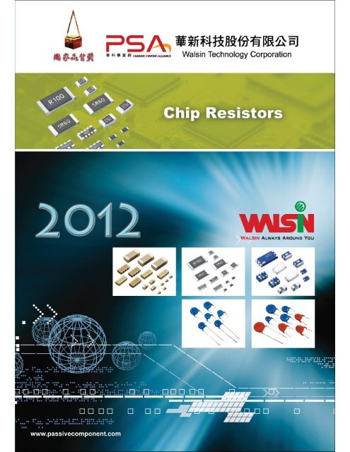
www.passivecomponent.com<br />
Chip Resistors<br />
HOW TO ORDER<br />
WR 12 X 1000 F T L<br />
Type code Size code Functional code Resistance Tolerance Packaging code Termination code<br />
WR : General 1~10MR 25 : 2512 (6432) X : 5% for 1 ~ 10M E24(J tol.) : 2 significant digits F : ± 1% P : 4" reel taping L = Sn base (Lead free)<br />
MR: Automotive 20 : 2010 (5025) 1% for 10 ~ 1M followed by No. of zeros and J : ± 5% T : 7" reel taping R = Pb 100ppm (total)<br />
SR: Anti-Sulfuration 18 : 1218 (3248) W : 1% for 1M a blank P : Jumper A : 7" reel taping 15Kpcs W = Wide term.<br />
ZR: Non magnetic 12 : 1206 (3216) Y : 5% for 1 ~ 10M (Low profile) e.g. : 3ohm = 3R0_ D : 7" reel taping 20Kpcs<br />
10 : 1210 (3225) 1% for 10 ~ 1M (Low profile) 10ohm = 100_ E : 7" up side down taping<br />
08 : 0805 (2012)<br />
Z : 1% for 1M<br />
(Low profile) 220ohm = 221_ V : 7" reel taping 1Kpcs<br />
06 : 0603 (1608) 56Kohm = 563_ Q : 10" reel taping<br />
04 : 0402 (1005)<br />
F: TC100 1-10ohm, 1%<br />
E: TC100, 100-1Mohm, 5% ("_" means blank) G : 13" reel taping<br />
02 : 0201 (0603) E24+E96 (F tol.) : 3 significant H : 0402-50K/13" reel<br />
01 : 01005 (0402) digits followed by No. of zeros R : 0603 2mm pitch taping<br />
e.g. : 3 = 3R00<br />
B : Bulk<br />
10 = 10R0<br />
K : Bulkcase<br />
220 = 2200<br />
C : Bulk after measuring<br />
56K = 5602<br />
WW 12 M R002 F T L<br />
Type code Size code Functional code Resistance Tolerance Packaging code Termination code<br />
WW: R < 1 25 : 2512 (6432) X : Thick film low ohm R followed by 3 significant digitsF : ± 1% P : 4" reel taping L = Sn base (Lead free)<br />
MW: R < 1, AUTO 20 : 2010 (5025) W : Thick film low ohm low TCR e.g. : G : ± 2% T : 7" reel taping G = Au base<br />
SW: R < 1, Anti-Sulfu 18 : 1218 (3248) Q : Metal low ohm 0.1 = R100 J : ± 5% Q : 10" reel taping S = Ag base<br />
12 : 1206 (3216) M : Metal low ohm 0.033 = R033 G : 13" reel taping<br />
10 : 1210 (3225) R : Metal low ohm high power 0.56 = R560 R : 0603 2mm pitch taping<br />
08 : 0805 (2012) N : Metal low ohm high power B : Bulk<br />
06 : 0603 (1608) P : Thick film low TCR high Power K : Bulkcase<br />
04 : 0402 (1005) 2512 = 2W<br />
2010 = 1W<br />
1210 = 0.5W<br />
1206 = 0.5W<br />
C : Thick film Power low ohm<br />
up side down<br />
WF 12 T 1001 B T L<br />
Type code Size code Functional code Resistance Tolerance Packaging code Termination code<br />
WF : Special function 25 : 2512 (6432) G : High ohm (>10M) E24(J tol.) : 2 significant digits A : ± 0.05% P : 4" reel taping L = Sn base (Lead free)<br />
MF : Special function AUTO 20 : 2010 (5025) H : Thick film, High Precision
Chip Resistors<br />
www.passivecomponent.com<br />
Chip Resistor Selection Guide<br />
General Purpose Chip-R<br />
Series Size Rated Power TCR (ppm/)* Tolerance Resistance<br />
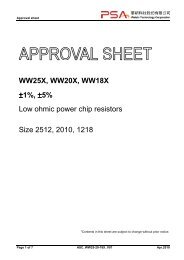
WR25X 2512 (6432) 1W<br />
±100 ±1%<br />
±200 ±5%<br />
WR18X 1218 (3248) 1W<br />
±100 ±1%<br />
±200 ±5%<br />
WR20X 2010 (5025) 1/2W<br />
±100 ±1%<br />
±200 ±5%<br />
WR10X 1210 (3225) 1/3W<br />
±100 ±1%<br />
±200 ±5%<br />
WR12X 1206 (3216) 1/4W<br />
±100 ±1%<br />
±200 ±5%<br />
1 ~ 10M<br />
WR08X 0805 (2012) 1/8W<br />
±100 ±1%<br />
±200 ±5%<br />
WR06X 0603 (1608) 1/10W<br />
±100 ±1%<br />
±200 ±5%<br />
WR04X 0402 (1005) 1/16W<br />
±100 ±1%<br />
±200 ±5%<br />
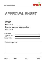
WR02X 0201 (0603) 1/20W<br />
±200 ±1%<br />
±200 ±5%<br />
WR01X 01005 (0402) 1/32W<br />
±200 ±1%<br />
±200 ±5%<br />
4.7 ~ 1M<br />
Remark: 1. Detailed resistance vs. TCR and ordering code please refer to specific specifications.<br />
2. Jumper resistor is not designed for fusing applications, designers shall apply dedicate fusible resistor or standard fuse in application circuits.<br />
Thick Film Low Ohm Chip-R<br />
Series Size Rated Power TCR (ppm/) Tolerance Resistance<br />
WW25X 2512 (6432) 1W<br />
±1% 0.020 ~ 0.976<br />
±5% 0.015 ~ 0.976<br />
WW18X 1218 (3248) 1W<br />
1500**<br />
±1% 0.020 ~ 0.976<br />
±5% 0.015 ~ 0.976<br />
WW20X 2010 (5025) 1/2W<br />
±1% 0.020 ~ 0.976<br />
±5% 0.015 ~ 0.976<br />
WW10X 1210 (3225) 1/3W 200<br />
±1% 0.020 ~ 0.976<br />
±5% 0.020 ~ 0.976<br />
WW12X 1206 (3216) 1/4W 1500**<br />
±1% 0.020 ~ 0.976<br />
±5% 0.020 ~ 0.976<br />
WW08X 0805 (2012) 1/8W 1500**<br />
±1% 0.020 ~ 0.976<br />
±5% 0.020 ~ 0.976<br />
WW06X 0603 (1608) 1/10W 500**<br />
±1% 0.100 ~ 0.976<br />
±5% 0.100 ~ 0.976<br />
WW04X 0402 (1005) 1/16W 600**<br />
±1% 0.100 ~ 0.976<br />
±5% 0.100 ~ 0.976<br />
Remark: 1. Detailed resistance vs. TCR and ordering code please refer to specific specifications.<br />
2. Resistance value will be changed by soldering condition and design of soldering pad, please design products in consideration of this change.<br />
Thick Film Power Low Ohm Chip-R<br />
Series Size Rated Power TCR (ppm/) Tolerance Resistance<br />
WW25P 2512 (6432) 2W<br />
WW20P 2010 (5025) 1W<br />
WW10P 1210 (3225) 1/2W<br />
WW12P 1206 (3216) 1/2W<br />
WW08P 0805 (2012) 1/3W<br />
WW06P 0603 (1608) 1/4W<br />
WW04P 0402 (1005) 1/8W<br />
WW08C 0805 (2012) 1/3W<br />
WW06C 0603 (1608) 1/4W<br />
WW04C 0402 (1005) 1/8W<br />
< 0.1: 150ppm<br />
±1% 0.047 ~ 0.976<br />
0.1: 100ppm ±5% 0.047 ~ 0.976<br />
< 0.1: 150ppm<br />
±1% 0.047 ~ 0.976<br />
0.1: 100ppm ±5% 0.047 ~ 0.976<br />
< 0.1: 500ppm<br />
±1% 0.020 ~ 0.976<br />
0.1: 200ppm ±5% 0.020 ~ 0.976<br />
< 0.1: 200ppm<br />
±1% 0.047 ~ 0.976<br />
0.1: 100ppm ±5% 0.047 ~ 0.976<br />
< 0.1: 200ppm<br />
±1% 0.047 ~ 0.976<br />
0.1: 150ppm ±5% 0.047 ~ 0.976<br />
< 0.1: 250ppm<br />
±1% 0.047 ~ 0.976<br />
0.1: 200ppm ±5% 0.047 ~ 0.976<br />
< 0.1: 300ppm<br />
±1% 0.100 ~ 0.976<br />
0.1: 200ppm ±5% 0.100 ~ 0.976<br />
< 0.03: 0~+250ppm ±1% 0.020 ~ 0.050<br />
0.03: ±150ppm ±5% 0.020 ~ 0.050<br />
< 0.051: 0~+250ppm ±1% 0.020 ~ 0.100<br />
0.051: ±150ppm ±5% 0.020 ~ 0.100<br />
< 0.051: 0~+350ppm ±1% 0.025 ~ 0.100<br />
0.051: ±150ppm ±5% 0.025 ~ 0.100<br />
2
www.passivecomponent.com<br />
Chip Resistors<br />
Metal Low Ohm Sensing Type Chip-R<br />
Remark:<br />
Series Size Rated Power TCR (ppm/)* Tolerance Resistance<br />
WW25N 2W ±100 ±1%, ±5% 1 ~ 25m*<br />
WW25R 2W ±100 ±1%, ±5% 1, 2, 3, 4, 5, 6, 7, 10m<br />
WW25M 2512 (6432)<br />
1W ±100 ±1%, ±5% 1 ~ 50m*<br />
WW25Q<br />
1W ±100 ±1%, ±5%<br />
1, 2, 3, 4, 5, 6, 7, 8, 9, 10,<br />
11, 12, 13, 14, 15m<br />
WW20N 2010 (5025) 1W ±75 ±1%, ±5% 5, 10, 15, 20m<br />
WW12N 1W ±70 ±1%, ±5% 5, 10, 15, 20, 25m<br />
WW12R 1206 (3216)<br />
1W ±100 ±1%, ±5% 1, 4, 5, 6, 8, 10, 15m<br />
WW12D<br />
1W ±100 ±1%, ±5% 20, 25, 30, 40, 50m<br />
WW08R 0805 (2012) 1/2W ±100 ±1%, ±5% 4, 5, 10m<br />
WW08D 0805 (2012) 1/2W ±100 ±1%, ±5% 20, 25, 30, 40, 50m<br />
WW06R 0603 (1608) 1/3W ±100 ±1%, ±5% 5, 10, 15m<br />
1. Detailed resistance vs. TCR and ordering code please refer to specific specifications.<br />
2. Resistance value will be changed by soldering condition and design of soldering pad, please design products in consideration of this change.<br />
Chip Resistor Array<br />
Series Size Rated Power TCR (ppm/) Termination Tolerance Resistance<br />
WA06X 1206 (0603x4) 1/10W ±200 Convex ±1%, ±5%<br />
WA06T 1206 (0603x4) 1/10W ±200 Concave ±1%, ±5%<br />
Remark:<br />
WA06Y 0606 (0603x2) 1/10W ±200 Convex ±1%, ±5%<br />
WA04X 0804 (0402x4) 1/16W ±200 Convex ±1%, ±5%<br />
10 ~ 1M<br />
WA04T 0804 (0402x4) 1/16W ±300 Concave ±1%, ±5%<br />
WA04Y 0404 (0402x2) 1/16W ±200 Convex ±1%, ±5%<br />
WA04U 0404 (0402x2) 1/16W ±300 Concave ±1%, ±5%<br />
WA06W 1606 (0402x8) 1/16W ±200 Convex ±1%, ±5% 10 ~ 100K<br />
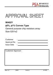
WA02Y 0806 (0201x2) 1/32W ±300 Convex ±1%, ±5% 10 ~ 1M<br />
Chip Attenuator<br />
1. Detailed resistance vs. TCR and ordering code please refer to specific specifications.<br />
2. Resistance value will be changed by soldering condition and design of soldering pad, please design products in consideration of this change.<br />
Series Size Type Termination Tolerance Attenuation Impedance<br />
WA04P 0404 (0402x2) 4P3R, type Convex ±0.1dB ~ 2.5dB 0, 0.5dB ~ 20dB 50<br />
Chip Resistor Network<br />
Series Size Rated Power TCR (ppm/) Termination Tolerance Resistance<br />
WT04X 1206 (10P8R) 1/16W ±200 Convex ±5% 10 ~ 100K<br />
High Power Chip-R<br />
Series Size Rated Power TCR (ppm/) Tolerance Resistance<br />
WF25P 2512 (6432) 2W ±100<br />
WF20P 2010 (5025) 1W ±100<br />
WF10P 1210 (3225) 1/2W ±100<br />
WF12P 1206 (3216) 1/2W ±100<br />
WF08P 0805 (2012) 1/4W ±100<br />
WF06P 0603 (1608) 1/8W ±100<br />
WF04P 0402 (1005) 1/8W ±100<br />
±1%, ±5% Jumper; 1 ~ 1M<br />
Automotive Chip-R<br />
Series Size Rated Power TCR(ppm/) Tolerance Resistance<br />
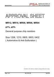
MR12 1206 (3216) 1/4W ±200 1~ 10M<br />
MR08 0805 (2012) 1/8W ±200 1~ 10M<br />
±1%, ±5%<br />
MR06 0603 (1608) 1/10W ±200 1~ 10M<br />
MR04 0402 (1005) 1/16W ±200<br />
1~ 10M<br />
Anti-Sulfuration Chip-R<br />
Series Size Rated Power TCR(ppm/) Tolerance Resistance<br />
SR12 1206 (3216) 1/4W 200 ±1%, ±5% 1~ 10M<br />
SR08 0805 (2012) 1/8W 200 ±1%, ±5% 1~ 10M<br />
SR06 0603 (1608) 1/10W 200 ±1%, ±5% 1~ 10M<br />
SR04 0402 (1005) 1/16W 200 ±1%, ±5% 1~ 10M<br />
Surge Chip-R<br />
Series Size Rated Power TCR(ppm/) Tolerance Resistance<br />
WK25S 2512 (6432) 1W 200 ±5%, ±10% 0.27 ~ 22M<br />
WK20S 2010 (5025) 3/4W 200 ±5%, ±10% 0.27 ~ 22M<br />
WK10S 1210 (3225) 1/2W 200 ±5%, ±10% 0.27 ~ 22M<br />
WK12S 1206 (3216) 1/4W 200 ±5%, ±10% 0.27 ~ 22M<br />
WK08S 0805 (2012) 1/8W 200 ±5%, ±10% 0.27 ~ 22M<br />
3
Chip Resistors<br />
www.passivecomponent.com<br />
High Voltage Chip-R<br />
Series Size Rated Power TCR(ppm/) Voltage (V) Tolerance Resistance<br />
WK25Z 2512 (6432) 1W 200 2000 ±5%, ±10%, ±20% 4.7M ~ 16M<br />
WK20Z 2010 (5025) 1/2W 200 1500 ±5%, ±10%, ±20% 1M ~ 16M<br />
WK25V 2512 (6432) 1W 200 800 ±1%, ±5% 47~ 51M<br />
WK20V 2010 (5025) 1/2W 200 500 ±1%, ±5% 47~ 51M<br />
WK12V 1206 (3216) 1/4W 200 500 ±1%, ±5% 47~ 51M<br />
WK08V 0805 (2012) 1/8W 200 400 ±1%, ±5% 47~ 51M<br />
WK06V 0603 (1608) 1/10W 200 200 ±1%, ±5% 47~ 10M<br />
Trimmable Chip-R<br />
Series Size Rated Power TCR(ppm/) Tolerance Resistance<br />
WK25M 2512 (6432) 1W 200 0/-20%, 0/-30% 1 ~ 4.7M<br />
WK20M 2010 (5025) 1/2W 200 0/-20%, 0/-30% 1 ~ 4.7M<br />
WK10M 1210 (3225) 1/4W 200 0/-20%, 0/-30% 1 ~ 4.7M<br />
WK12M 1206 (3216) 1/8W 200 0/-20%, 0/-30% 1 ~ 4.7M<br />
WK08M 0805 (2012) 1/10W 200 0/-20%, 0/-30% 1 ~ 4.7M<br />
WK06M 0603 (1608) 1/16W 100 0/-20%, 0/-30% 10~ 4.7M<br />
Total lead free Chip-R ( Pb < 100ppm )<br />
Series Size Rated Power TCR(ppm/) Tolerance Resistance<br />
WR12X_R 1206 (3216) 1/4W 200 ±1%, ±5% 1~ 10M<br />
WR08X_R 0805 (2012) 1/8W 200 ±1%, ±5% 1~ 10M<br />
WR06X_R 0603 (1608) 1/10W 200 ±1%, ±5% 1~ 10M<br />
WR04X_R 0402 (1005) 1/16W 200 ±1%, ±5% 1~ 10M<br />
WA04X_R 0402X4 1/16W 200 ±1%, ±5% 10 ~ 1M<br />
WA04Y_R 0402X2 1/16W 200 ±1%, ±5% 10 ~ 1M<br />
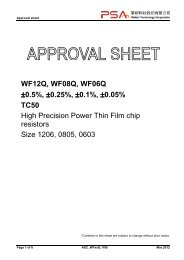
High Precision Chip-R<br />
Series Size Rated Power TCR(ppm/) Tolerance Resistance<br />
WF12H 1206 (3216) 1/4W 100 ±0.1%, ±0.5% 10 ~ 1M<br />
WF08H 0805 (2012) 1/8W 100 ±0.1%, ±0.5% 10 ~ 1M<br />
WF06H 0603 (1608) 1/10W 100 ±0.1%, ±0.5% 10 ~ 1M<br />
WF04H 0402 (1005) 1/16W 100 ±0.1%, ±0.5% 10 ~ 1M<br />
WF25T 2512 (6432) 3/4W 50 ±0.05%, ±0.10%,±0.25%, ±0.50%, ±1.0% 10 ~ 1.5M<br />
WF25Q 2512 (6432) 1W 50 ±0.05%, ±0.10%,±0.25%, ±0.50%, ±1.0% 10 ~ 1.5M<br />
WF20T 2010 (5025) 1/2W 50 ±0.05%, ±0.10%,±0.25%, ±0.50%, ±1.0% 10 ~ 1.5M<br />
WF20Q 2010 (5025) 3/4W 50 ±0.05%, ±0.10%,±0.25%, ±0.50%, ±1.0% 10 ~ 1.5M<br />
WF10T 1210 (3225) 1/4W 50 ±0.05%, ±0.10%,±0.25%, ±0.50%, ±1.0% 10 ~ 1M<br />
WF10Q 1210 (3225) 2/5W 50 ±0.05%, ±0.10%,±0.25%, ±0.50%, ±1.0% 10 ~ 1M<br />
WF12T 1206 (3216) 1/8W 50 ±0.05%, ±0.10%,±0.25%, ±0.50%, ±1.0% 4.7 ~ 1M<br />
WF12Q 1206 (3216) 1/4W 50 ±0.05%, ±0.10%,±0.25%, ±0.50%, ±1.0% 4.7 ~ 1M<br />
WF08T 0805 (2012) 1/10W 50 ±0.05%, ±0.10%,±0.25%, ±0.50%, ±1.0% 4.7 ~ 1M<br />
WF08Q 0805 (2012) 1/8W 50 ±0.05%, ±0.10%,±0.25%, ±0.50%, ±1.0% 4.7 ~ 1M<br />
WF06T 0603 (1608) 1/16W 50 ±0.05%, ±0.10%,±0.25%, ±0.50%, ±1.0% 4.7 ~ 680K<br />
WF06Q 0603 (1608) 1/10W 50 ±0.05%, ±0.10%,±0.25%, ±0.50%, ±1.0% 4.7 ~ 680K<br />
WF04T 0402 (1005) 1/16W 50 ±0.05%, ±0.10%,±0.25%, ±0.50%, ±1.0% 10 ~ 100K<br />
WF25U 2512 (6432) 3/4W 25 ±0.05%, ±0.10%,±0.25%, ±0.50%, ±1.0% 10 ~ 1.5M<br />
WF25R 2512 (6432) 1W 25 ±0.05%, ±0.10%,±0.25%, ±0.50%, ±1.0% 10 ~ 1.5M<br />
WF20U 2010 (5025) 1/2W 25 ±0.05%, ±0.10%,±0.25%, ±0.50%, ±1.0% 10 ~ 1.5M<br />
WF20R 2010 (5025) 3/4W 25 ±0.05%, ±0.10%,±0.25%, ±0.50%, ±1.0% 10 ~ 1.5M<br />
WF10U 1210 (3225) 1/4W 25 ±0.05%, ±0.10%,±0.25%, ±0.50%, ±1.0% 10 ~ 1M<br />
WF10R 1210 (3225) 2/5W 25 ±0.05%, ±0.10%,±0.25%, ±0.50%, ±1.0% 10 ~ 1M<br />
WF12U 1206 (3216) 1/8W 25 ±0.05%, ±0.10%,±0.25%, ±0.50%, ±1.0% 4.7 ~ 1M<br />
WF12R 1206 (3216) 1/4W 25 ±0.05%, ±0.10%,±0.25%, ±0.50%, ±1.0% 4.7 ~ 1M<br />
WF08U 0805 (2012) 1/10W 25 ±0.05%, ±0.10%,±0.25%, ±0.50%, ±1.0% 4.7 ~ 1M<br />
WF08R 0805 (2012) 1/8W 25 ±0.05%, ±0.10%,±0.25%, ±0.50%, ±1.0% 4.7 ~ 1M<br />
WF06U 0603 (1608) 1/16W 25 ±0.05%, ±0.10%,±0.25%, ±0.50%, ±1.0% 4.7 ~ 680K<br />
WF06R 0603 (1608) 1/10W 25 ±0.05%, ±0.10%,±0.25%, ±0.50%, ±1.0% 4.7 ~ 680K<br />
WF04U 0402 (1005) 1/16W 25 ±0.05%, ±0.10%,±0.25%, ±0.50%, ±1.0% 10 ~ 100K<br />
WF12F 1206 (3216) 1/8W 15 ±0.05%, ±0.10%,±0.25% 100 ~ 200K<br />
WF08F 0805 (2012) 1/8W 15 ±0.05%, ±0.10%,±0.25% 100 ~ 200K<br />
WF06F 0603 (1608) 1/10W 15 ±0.05%, ±0.10%,±0.25% 100 ~ 100K<br />
WF04F 0402 (1005) 1/16W 15 ±0.05%, ±0.10%,±0.25% 100 ~ 20K<br />
WF12W 1206 (3216) 1/8W 10 ±0.05%, ±0.10%,±0.25% 25 ~ 300K<br />
WF08W 0805 (2012) 1/8W 10 ±0.05%, ±0.10%,±0.25% 25 ~ 200K<br />
WF06W 0603 (1608) 1/10W 10 ±0.05%, ±0.10%,±0.25% 25 ~ 100K<br />
WF04W 0402 (1005) 1/16W 10 ±0.05%, ±0.10%,±0.25% 25 ~ 20K<br />
WF12Z 1206 (3216) 1/8W 5 ±0.05%, ±0.10%,±0.25% 25 ~ 120K<br />
WF08Z 0805 (2012) 1/8W 5 ±0.05%, ±0.10%,±0.25% 25 ~ 80K<br />
WF06Z 0603 (1608) 1/10W 5 ±0.05%, ±0.10%,±0.25% 25 ~ 40K<br />
WF04Z 0402 (1005) 1/16W 5 ±0.05%, ±0.10%,±0.25% 25 ~ 8K<br />
4
www.passivecomponent.com<br />
Chip Resistors<br />
General Purpose Chip Resistors (1~10M)<br />
Feature<br />
1. High reliability and stability<br />
2. Reduced size of final equipment<br />
3. Lower assembly costs<br />
4. Higher component and equipment reliability<br />
5. RoHs compliant and lead free products<br />
Description<br />
The resistors are constructed in a high grade ceramic body (aluminum oxide).<br />
Internal metal electrodes are added at each end and connected by a resistive<br />
paste that is applied to the top surface of the substrate. The composition of the<br />
paste is adjusted to give the approximate resistance required and the value is<br />
trimmed to within tolerance by laser cutting of this resistive layer.<br />
The resistive layer is covered with a protective coat. Finally, the two external end<br />
terminations are added. For ease of soldering the outer layer of these end<br />
terminations is Tin solder (Pb free) alloy.<br />
Quick Reference <strong>Data</strong><br />
Application<br />
1. Consumer electrical equipment, PDA Digital Camcorder,<br />
2. EDP, Computer application<br />
3. Mobile phone, Telecom<br />
4. Power supply, Battery charger, DC-DC power converter<br />
5. Digital meter<br />
6. Automotive.<br />
Series No. WR25X WR20X WR18X WR10X WR12X WR08X WR06X WR04X WR02X WR01X<br />
Size code 2512 (6432) 2010 (5025) 1218(3248) 1210 (3225) 1206 (3216) 0805(2012) 0603(1608) 0402(1005) 0201(0603) 01005(0402)<br />
Resistance Range<br />
±5% Tolerance (E24)<br />
±1% Tolerance<br />
(E24+E96)<br />
TCR (ppm/ )<br />
R>1M<br />
1MR10<br />
R10<br />
Max. dissipation @<br />
Tamb=70<br />
Max. Operation Voltage<br />
(DC or RMS)<br />
Climatic category (IEC<br />
60068)<br />
±200<br />
±100<br />
±200<br />
±200<br />
±100<br />
±200<br />
±5% (E24): 1~10M;Jumper<br />
±1% (E2+E964): 1~10M<br />
±200<br />
±200*<br />
±200<br />
±200<br />
±300<br />
±200<br />
±300<br />
1.0 W 1/2 W 1.0 W 1/3 W 1/4 W 1/8 W 1/10 W 1/16 W 1/20 W 1/32 W<br />
250V 200V 200V 200V 200V 150V 50V 50V 25V 20V<br />
Basic Specification JIS C 5201-1 / IEC 60115-1<br />
Note:<br />
1. This is the maximum voltage that may be continuously supplied to the resistor element, see “IEC publication 60115-8”.<br />
2. Max. Operation Voltage: So called RCWW (Rated Continuous Working Voltage) is determined by<br />
RCWV=Rater Power ×Resistance Value or Max. RCWV listed above, whichever is lower.<br />
3. Detailed TCR please refer to specific specification.<br />
55/155/56 55/125/56<br />
Physical Dimensions<br />
Unit: mm<br />
Size<br />
2512<br />
(6432)<br />
2010<br />
(5025)<br />
1218<br />
(3248)<br />
1210<br />
(3225)<br />
1206<br />
(3216)<br />
0805<br />
(2012)<br />
0603<br />
(1608)<br />
0402<br />
(1005)<br />
0201<br />
(0603)<br />
01005<br />
(0402)<br />
L 6.40±0.20 5.00±0.20 3.05±0.15 3.10±0.10 3.10±0.10 2.00±0.10 1.60±0.10 1.00±0.05 0.60±0.03 0.40±0.02<br />
W 3.20±0.20 2.50±0.20 4.60±0.20 2.60±0.10 1.60±0.10 1.25±0.10 0.80±0.10 0.50±0.05 0.30±0.03 0.20±0.02<br />
T 0.60±0.10 0.55±0.10 0.55±0.10 0.55±0.10 0.60±0.15 0.50±0.15 0.45±0.15 0.35±0.05 0.23±0.03 0.13±0.02<br />
Tb 0.90±0.25 0.60±0.25 0.50±0.25 0.50±0.20 0.45±0.20 0.40±0.20 0.30±0.15 0.25±0.10 0.15±0.05 0.10±0.03<br />
Tt 0.65±0.25 0.65±0.25 0.45±0.25 0.50±0.20 0.50±0.20 0.40±0.20 0.30±0.10 0.20±0.10 0.50±0.20 0.08±0.03<br />
Power Deration Curve<br />
For resistors operated in ambient temperature over 70, power rating should be derated in accordance with the following figures.<br />
5
Chip Resistors<br />
www.passivecomponent.com<br />
Thick Film Low Ohm/Power Low Ohm Chip Resistors<br />
Function For Low Ohm Chip Resistors<br />
The low ohmic resistors are used to sense output current in power supply,<br />
automotive and engine control management system, and other power<br />
sensing application. As shows in figure below, the typical function of low<br />
ohmic (power) chip resistor is to be a current sensor (Rsense) to generate<br />
the sensing voltage (Vs) for the purpose of feedback control when output<br />
current (lo) passed on it . The sensing voltage be treated as a signal to<br />
trigger the switches (CMOS) ON/OFF duration so that to monitor and/or<br />
adjust the output current from inductor.<br />
Simplify to say, Vs=Io ×Rsense.<br />
In general case, this feedback voltage is setting around 100mV for<br />
considering both on power saving and noise robustness. To sense a 5<br />
ampere average output current, the Rsense resistance value therefore be<br />
required as 100mV / 5A = 20 m, the power dissipation will be :<br />
P=I2 ×R =5A2 ×20m =0.5Watt<br />
A low ohmic chip resistor with a power rating of 1.0 watt is recommended<br />
on this application in case the power safety margin is taken into account.<br />
Quick Reference <strong>Data</strong> of Low Ohm Chip Resistor<br />
Series No. WW25X WW20X WW18X WW10X WW12X WW08X WW06X WW04X<br />
Size code<br />
2512<br />
(6432)<br />
2010<br />
(5025)<br />
1218<br />
(3248)<br />
1210<br />
(3225)<br />
1206<br />
(3216)<br />
0805<br />
(2012)<br />
0603<br />
(1608)<br />
0402<br />
(1005)<br />
Resistance Tolerance ±5% , ±1%<br />
Resistance Range 0.020 ~ 0.976 0.100 ~ 0.976<br />
TCR (ppm/)<br />
Detailed TCR please refer to specific data <strong>sheet</strong>s<br />
Max. dissipation @ Tamb=70 1 Watt 0.5 Watt 1 Watt 1/3 Watt 1/4 Watt 1/8 Watt 1/10 Watt 1/16 Watt<br />
Max. Operation Voltage (DC or RMS) 250V 200V 200V 200V 200V 100V 50V 50V<br />
Climatic category (IEC 60068) 55/155/56 55/125/56<br />
Basic Specification JIS C 5201-1 / IEC 60115-1<br />
Note :<br />
1. This is the maximum voltage that may be continuously supplied to the resistor element, see “IEC publication 60115-9” .<br />
2. Power derating curve, and detail specification please refer to specific data <strong>sheet</strong>s.<br />
3. Resistance value will be changed by soldering condition and design of solding pad, please design products in consideration of change of resistance value.<br />
Quick Reference <strong>Data</strong> of Power Low Ohm Chip Resistor<br />
Item<br />
General Specification<br />
Series No. WW25P WW20P WW12P WW08P WW06P WW04P<br />
Size code 2512 (6432) 2010 (5025) 1206 (3216) 0805(2012) 0603(1608) 0402(1005)<br />
Resistance Tolerance ±5% , ±1%<br />
Resistance Range 0.047 ~ 0.976 0.1~0.976<br />
TCR (ppm/) 0.100 ±150ppm/ ±150ppm/ ±200ppm/ ±200ppm/ ±250ppm/ -<br />
0.100 ±100ppm/ ±100ppm/ ±100ppm/ ±150ppm/ ±200ppm/ 0~+300ppm/<br />
Max. dissipation @ Tamb=70 2 W 1 W 1/2 W 1/3 W 1/4 W 1/8 W<br />
Max. Operation Voltage (DC or RMS) 300V 200V 200V 150V 50V 50V<br />
Climatic category (IEC 60068) 55/155/56 55/125/56<br />
Note :<br />
1. This is the maximum voltage that may be continuously supplied to the resistor element, see “IEC publication 60115-8” .<br />
2. Max. Operation Voltage : So called RCWW (Rated Continuous Working Voltage) is determined by<br />
RCWV=Rater Power Resistance Value or Max. RCWV listed above, whichever is lower.<br />
3. 2W loading with total solder-pad and trace size of 300mm2<br />
Physical Dimensions<br />
Unit: mm<br />
Dimensions WW25P WW20P WW12P WW08P WW06P WW04P<br />
L 6.30±0.20 5.00±0.20 3.10±0.15 2.00±0.15 1.60±0.10 1.00±0.05<br />
W 3.10±0.20 2.50±0.20 1.60±0.15 1.20±0.15 0.80±0.10 0.50±0.05<br />
T 0.60±0.15 0.60±0.10 0.55±0.10 0.50±0.10 0.45±0.10 0.35±0.05<br />
Tt 0.60±0.25 0.60±0.25 0.50±0.25 0.40±0.20 0.30±0.20 0.20±0.10<br />
Tb 1.80±0.25 0.65±0.25 0.50±0.25 0.40±0.20 0.30±0.20 0.25+0.05/-0.1<br />
6
www.passivecomponent.com<br />
Chip Resistors<br />
Metal Low Ohm Sensing Chip Resistors (0.001~ 0.050)<br />
Description<br />
The resistors are constructed in a high grade low resistive metal body. The resistive<br />
layer is covered with a protective coat and printed a resistance marking code over it.<br />
Finally, the two external end terminations are added. For ease of soldering the outer<br />
layer of these end terminations is a lead free terminations.<br />
Quick Reference <strong>Data</strong><br />
Item<br />
General Specification<br />
Series No. WW25R WW25Q WW12R WW12D WW08D WW06R<br />
Size code 2512 (6432) 1206(3216) 0805 (2012) 0603 (1608)<br />
Resistance Tolerance ±5% , ±1%<br />
Resistance Range 1,2,3,4,5,6,7,10m 1 ~ 15m<br />
1,4, 5, 6, 8, 10,<br />
15m<br />
20, 25, 30, 40,<br />
50m<br />
20, 25, 30, 40,<br />
50m<br />
5, 10, 15m<br />
TCR (ppm/) ±100ppm ±100ppm ±100ppm ±100ppm<br />
Max. dissipation @ Tamb=70 2 W 1 W 1 W 1 W 1/2 W 1/3 W<br />
Max. Operation Current (DC or RMS) 44.7A 14A 5A 8.1A<br />
Climatic category (IEC 60068) 55/155/56<br />
Item<br />
General Specification<br />
Series No. WW25M WW25N WW20M WW20N WW12N WW12M<br />
Size code 2512 (6432) 2010 (5025) 1206(3216)<br />
Resistance Tolerance ±5% , ±1%<br />
Resistance Range<br />
1~10, 12, 15, 20,<br />
25, 30, 40, 50m<br />
1~10, 12, 15, 20,<br />
25m<br />
5, 10, 15, 20m 5, 10, 15, 20, 25m<br />
TCR (ppm/) 1-4m: ±100ppm; > 4m: ± 75 ppm/ 75 ppm/ 70 ppm/<br />
Max. dissipation @ Tamb=70 1 W 2 W 1/2 W 1 W 1 W 1/2 W<br />
Max. Operation Voltage (DC or RMS) 250V 250V 200V<br />
Max. Overload Voltage (DC or RMS) 500V 500V 400V<br />
Climatic category (IEC 60068) 55/155/56<br />
Note :<br />
1. This is the maximum voltage that may be continuously supplied to the resistor element, see “IEC publication 60115-8” .<br />
2. Power derating curve, and detail specification please refer to specific data <strong>sheet</strong>s.<br />
3. Resistance value will be changed by soldering condition and design of solding pad, please design products in consideration of chang of resistance value.<br />
Physical Dimensions:<br />
WW25M(0.002~0.025), WW25N(0.003~0.025), WW20N, WW12N<br />
Unit: mm<br />
Symbol 2512 2010 1206<br />
L 6.40±0.20 5.00±0.20 3.10±0.20<br />
W 3.20±0.20 2.50±0.20 1.60±0.20<br />
T 0.60±0.15 0.60±0.15 0.60±0.25<br />
Tt 0.65±0.25 0.65±0.25 0.60±0.20<br />
Tb 0.65±0.25 0.65±0.25 0.60±0.20<br />
WW25M(0.001), WW25N(0.001~0.002)<br />
Symbol 2512<br />
L 6.40±0.20<br />
W 3.20±0.20<br />
T 0.60±0.10<br />
Tt 1.60±0.25<br />
Tb 1.60±0.25<br />
Unit: mm<br />
WW25Q, WW25R, WW12R, WW12D, WW06R<br />
Note : 1. The detailed dimensions please refer to data <strong>sheet</strong> per type!<br />
7
Chip Resistors<br />
www.passivecomponent.com<br />
Chip Resistors Array : Convex Termination<br />
Feature<br />
Application<br />
1. High reliability and stability 1. Consumer electrical equipment, PDA Digital Camcorder,<br />
2. Reduced size of final equipment 2. EDP, Computer application<br />
3. Lower assembly cost and higher surface mounted efficiency 3. Mobile phone, Telecom<br />
4. Higher component and equipment reliability 4. DIMM<br />
Description and Physical Dimensions<br />
The resistors array is constructed in a high grade ceramic body (aluminum oxide). Internal metal<br />
electrodes are added at each end and connected by a resistive paste that is applied to the top<br />
surface of the substrate. The composition of the paste is adjusted to give the approximate<br />
resistance required and the value is trimmed to within tolerance by laser cutting of this resistive<br />
layer.<br />
The resistive layer is covered with a protective coat. Finally, the two external end terminations are<br />
added. For ease of soldering the outer layer of these end termination is Tin solder alloy. Marking<br />
code description is depended on component size and tolerance. Following figure shown the<br />
construction of a Chip-R array.<br />
Physical Dimensions<br />
Unit: mm<br />
Type WA06X WA04X WA06Y WA04Y<br />
L 3.20±0.10 2.00±0.10 1.60±0.10 1.00±0.10<br />
W 1.60±0.10 1.00±0.10 1.50±0.10 1.00±0.10<br />
T 0.50±0.10 0.45±0.10 0.50±0.10 0.35±0.10<br />
P 0.80±0.10 0.50±0.05 1.00±0.10 0.65±0.10<br />
A 0.60±0.10 0.40±0.10 0.60±0.10 0.34±0.10<br />
B 0.30±0.10 0.20±0.10 0.30±0.15 0.20±0.15<br />
C 0.40±0.10 0.30±0.05 - -<br />
G 0.30±0.20 0.25±0.10 0.30±0.15 0.25±0.17<br />
Quick Reference <strong>Data</strong><br />
Series No. WA06X WA04X WA06Y WA04Y<br />
Size 0603×4(1608×4) 0402×4(1005×4) 0603×2(1608×4) 0402×2(1005×2)<br />
Termination construction 8P4R,Convex 4P2R,Convex<br />
Resistance Tolerance<br />
Resistance Range<br />
±5%, ±1% (E24 series)<br />
10~1M(E24 series), Jumper (0)<br />
TCR (ppm/) ±200 ppm/ ±300 ppm/<br />
Max. dissipation @ Tamb=70 1/10 Watt 1/16 Watt 1/10 Watt 1/16 Watt<br />
Max. Operation Voltage (DC or RMS) 50V 50V 1/10 Watt 1/16 Watt<br />
Max. Overload Voltage (DC or RMS) 100V 100V 1/10 Watt 1/16 Watt<br />
Climatic category (IEC 60068) 55/155/56 55/125/56<br />
Basic Specification JIS C5201-1 / IEC 60115-1<br />
Circuit Mode: R1=R2(=R3=R4)<br />
Note :<br />
Power derating curve and detail specification please refer to specific data <strong>sheet</strong>s.<br />
8
www.passivecomponent.com<br />
Chip Resistors<br />
WA06W Chip Resistors Array 16P8R<br />
Description<br />
The resistors array is constructed in a high grade ceramic body (aluminum oxide).<br />
Internal metal electrodes are added at each end and connected by a resistive paste that<br />
is applied to the top surface of the substrate. The composition of the paste is adjusted to<br />
give the approximate resistance required and the value is trimmed to within tolerance by<br />
laser cutting of this resistive layer.<br />
The resistors layer is covered with a protective coat. Finally, the two external end<br />
terminations are added. For ease of soldering the outer layer of these end termination is<br />
Tin (Pb free) solder alloy.<br />
Quick Reference <strong>Data</strong><br />
Item<br />
General Specification<br />
Series No. WA06W WA06W_N<br />
Size 1606 (0602×8) 1606 (0602×8)<br />
Termination construction Convex type Convex type<br />
Resistance Tolerance ±5% (E24 series) ±5% (E24 series)<br />
Resistance Range 10~100K, Jumper (0) 10~100K, Jumper (0)<br />
TCR (ppm/) ± 200 ppm/ ± 200 ppm/<br />
Max. dissipation @ Tamb=70 1/16 W 1/16 W<br />
Max. Operation Voltage (DC or RMS) 50V 25V<br />
Max. Overload Voltage (DC or RMS) 100V 50V<br />
Carrier Tape width 12mm 8mm<br />
Climatic category (IEC 60068) 55/125/56 55/125/56<br />
Circuit Mode:<br />
R1=R2=R3=R4=R5=R6=R7=R8<br />
Note :<br />
Power derating curve and detail specification please refer to specific data <strong>sheet</strong>s.<br />
Physical Dimensions:<br />
Unit: mm<br />
Symbol WA06W WA06W_N<br />
L 4.00±0.20 3.80±0.10<br />
W 1.60±0.15 1.60±0.10<br />
T 0.45±0.10 0.45±0.10<br />
B 0.30±0.20 0.30±0.10<br />
G 0.30±0.20 0.30±0.10<br />
D 0.20±0.10 0.20±0.10<br />
P 0.50±0.20 0.50±0.10<br />
H1 0.40±0.20 0.30±0.10<br />
H2 0.30±0.10 0.30±0.10<br />
9
Chip Resistors<br />
www.passivecomponent.com<br />
Chip Resistors Array : Concave Termination<br />
Feature<br />
Application<br />
1. High reliability and stability 1. Consumer electrical equipment, PDA Digital Camcorder,<br />
2. Reduced size of final equipment 2. EDP, Computer application<br />
3. Lower assembly cost and higher surface mounted efficiency 3. Mobile phone, Telecom<br />
4. Higher component and equipment reliability 4. DIMM<br />
5. Strong body and terminations<br />
6. Excellent performance in surface mounting assembly.<br />
Description and Physical Dimensions<br />
The resistor array is constructed in a high grade ceramic body (aluminum oxide).<br />
Internal metal electrodes are added at each end and connected by a resistive<br />
paste that is applied to the top surface of the substrate. The composition of the<br />
paste is adjusted to give the approximate resistance required and the value is<br />
trimmed to within tolerance by laser cutting of this resistive layer.<br />
The resistive layer is covered with a protective coat. Finally, the two external end<br />
terminations are added. For ease of soldering the outer layer of these end<br />
termination is Tin solder alloy. Marking code description is depended on<br />
component size and tolerance. Following figure shown the construction of a<br />
Chip-R array.<br />
Quick Reference <strong>Data</strong><br />
Item<br />
General Specification<br />
Series No. WA06T WA04T WA04U<br />
Size 0603×4 (1608×4) 0402×4 (1005×4) 0402×2 (1005×2)<br />
Termination construction<br />
Resistance Tolerance<br />
Resistance Range<br />
Concave type<br />
±5% , ±1% (E24 series)<br />
10~1M, Jumper (0)<br />
TCR (ppm/) ± 200 ppm/ ± 300 ppm/ ± 300 ppm/<br />
Max. dissipation @ Tamb=70 1/10 W 1/16 W 1/16 W<br />
Max. Operation Voltage (DC or RMS) 50V 25V 25V<br />
Max. Overload Voltage 100V 50V 50V<br />
Climatic category (IEC 60068) 55/125/56 55/125/56 55/125/56<br />
Circuit Mode<br />
L 3.20+0.20/-0.10mm 2.00±0.10mm 1.00±0.10mm<br />
W 1.60+0.20/-0.10mm 1.00±0.10mm 1.00±0.10mm<br />
T 0.60±0.20mm 0.45±0.10mm 0.30±0.10mm<br />
P 0.80±0.10mm 0.50±0.05mm 0.50±0.05mm<br />
A 0.60±0.15mm 0.35±0.05mm 0.35±0.10mm<br />
B 0.35±0.15mm 0.20±0.15mm 0.25±0.15mm<br />
C 0.50±0.15mm 0.25±0.05mm 0.35±0.10mm<br />
G 0.50±0.15mm 0.25±0.15mm 0.25±0.15mm<br />
Note :<br />
1. Power derating curve and detail specification please refer to specific data <strong>sheet</strong>s.<br />
2. Max. Operation Voltage : So called RCWW (Rated Continuous Working Voltage) is determined by<br />
RCWV = Rater Power Resistance Value or Max. RCWV listed above, whichever is lower.<br />
10
www.passivecomponent.com<br />
Chip Resistors<br />
WT04X Chip Resistor Network 10P8R<br />
Description<br />
The resistor array is constructed in a high grade ceramic body (aluminum oxide).<br />
Internal metal electrodes are added at each end and connected by a resistive<br />
paste that is applied to the top surface of the substrate. The composition of the<br />
paste is adjusted to give the approximate resistance required and the value is<br />
trimmed to within tolerance by laser cutting of this resistive layer.<br />
The resistive layer is covered with a protective coat. Finally, the two external end<br />
terminations are added. For ease of soldering the outer layer of these end<br />
termination is Tin (Pb free) solder alloy.<br />
Quick Reference <strong>Data</strong><br />
Item<br />
General Specification<br />
Series No.<br />
Size<br />
Termination construction<br />
Resistance Tolerance<br />
Resistance Range<br />
TCR (ppm/)<br />
Max. dissipation @ Tamb=70<br />
Max. Operation Voltage (DC or RMS)<br />
Max. Overload Voltage (DC or RMS)<br />
WT04X<br />
0402x8 (1005x8)<br />
Convex type<br />
±5% (E24 series)<br />
10 ~ 100K<br />
± 200 ppm/<br />
1/16 W<br />
25V<br />
50V<br />
Climatic category (IEC 60068) 55/155/56<br />
Circuit Mode:<br />
Resistor elements on pin1 ~ pin4, pin6 ~ pin9;<br />
R1=R2=R3=R4=R6=R7=R8=R9<br />
Note :<br />
1. Power derating curve and detail specification please refer to specific data <strong>sheet</strong>s.<br />
Physical Dimensions:<br />
Symbol<br />
L 3.30±0.20<br />
<br />
Unit: mm<br />
W 1.60±0.15<br />
T 0.55±0.10<br />
P 0.64±0.05<br />
A 0.50±0.05<br />
B 0.40±0.15<br />
C 0.40±0.15<br />
G 0.40±0.15<br />
11
Chip Resistors<br />
www.passivecomponent.com<br />
WA04P Chip Attenuator<br />
Typical Application of Chip Attenuator<br />
WA04 P 001 X B T L<br />
Size code<br />
WA04: 0402<br />
per element<br />
Type code<br />
P: convex, type<br />
attenuator<br />
Attenuation Range<br />
000 = 0dB<br />
R05 = 0.5dB<br />
001 = 1dB<br />
R15 = 1,5dB<br />
002 = 2dB<br />
003 = 3dB<br />
004 = 4dB<br />
005 = 5dB<br />
006 = 6dB<br />
007 = 7dB<br />
008 = 8dB<br />
009 = 9dB<br />
010 =10dB<br />
011 = 11dB<br />
012 = 12dB<br />
013 = 13dB<br />
014 = 14dB<br />
015 = 15dB<br />
016 = 16dB<br />
017 = 17dB<br />
018 = 18dB<br />
019 = 19dB<br />
020 = 20dB<br />
Characteristic Impedance<br />
X:50<br />
Attenuation Tolerance<br />
A : 0.1dB<br />
B : 0.3dB<br />
C : 0.4dB<br />
D : 0.8dB<br />
E : 1.0dB<br />
F : 1.5dB<br />
G : 2.0dB<br />
H : 2.5dB<br />
P : -<br />
Termination<br />
T=7'' reel taped<br />
Packaging<br />
L=Sn base<br />
(lead free)<br />
type Attenuator (-6dB, 50W) for VSWR improvement and output frequency level matching on VCO application.<br />
Quick Reference <strong>Data</strong><br />
Item<br />
General Specification<br />
Series No.<br />
WA04P<br />
Size 0402×2 (1005×2)<br />
Termination construction<br />
Convex type<br />
Attenuation Range<br />
Attenuation Tolerance<br />
0dB<br />
0.5dB<br />
1dB~ 5dB<br />
6dB~ 10dB<br />
11dB~ 13dB<br />
14dB<br />
15dB~ 16dB<br />
17dB~ 19dB<br />
20dB<br />
Characteristic impedance<br />
Rated power at Tamb=70<br />
Limiting Voltage (DC)<br />
Frequency range (DC)<br />
0dB, 0.5dB ~ 20dB<br />
-<br />
± 0.1dB<br />
± 0.3dB<br />
± 0.4dB<br />
± 0.8dB<br />
± 1.0dB<br />
± 1.5dB<br />
± 2.0dB<br />
± 2.5dB<br />
50<br />
0.1 W / package<br />
50V<br />
MAX. 3 GHz<br />
VSWR (Voltage Standing Wave Ratio) MAX. 1.2<br />
Number of Resistors<br />
Number of Terminals<br />
3 resistors<br />
4 terminals<br />
Climatic category (IEC 60068) -40 ~ 125’C<br />
Physical Dimensions:<br />
Unit: mm<br />
WA04P<br />
L 1.00±0.10<br />
W 1.00+0.10/-0<br />
T 0.35±0.10<br />
P 0.65±0.20<br />
A 0.33±0.10<br />
Ta 0.15±0.10<br />
Tb 0.25±0.10<br />
12
www.passivecomponent.com<br />
Chip Resistors<br />
Special Application Chip Resistors<br />
Feature<br />
1. Provided Automotive & Anti-sulfuration resistors (MR/SR series) for Auto & Anti-sulfuration application.<br />
2. Provided Total Lead Free resistors (WR_R series) to fulfill RoHS environmental regulation.<br />
3. Provided trimmable resistors (WKxxM series) for customer special tolerance requirement.<br />
4. Provided high precision tolerance (WFxxH/ WFxxT/ WFxxU/ WFxxW) down to 0.05% and TCR down to 10ppm/ for voltage sensing.<br />
5. High reliability and stability.<br />
6. Reduced size of final equipment<br />
7. Lower assembly costs.<br />
8. Higher component and equipment reliability<br />
9. Special resistance, tolerance are available upon customer's request.<br />
MR/SR Series of Automotive & Anti-sulfuration Chip Resistor<br />
Feature<br />
1. High reliability and stability ±1%.<br />
2. Sulfuration resistant<br />
3. Automotive grade AEC Q-200 compliant.<br />
4. 100% CCD inspection.<br />
5. RoHS compliant and lead free.<br />
Quick Reference <strong>Data</strong><br />
Application<br />
1. Automotive application.<br />
2. Consumer electrical equipment.<br />
3. EDP, Computer application.<br />
4. Telecom Application.<br />
Series No. MR12X MR08X MR06X MR04X<br />
Size code 1206(3126) 0805(2012) 0603(1608) 0402(1005)<br />
Resistance Range<br />
1~10M (±1% , ±5%) ,Jumper<br />
TCR (ppm/)<br />
±200 ppm*<br />
Max. dissipation @ Tamb=70 1/4 W 1/8 W 1/10 W 1/16 W<br />
Max. Operation Voltage (DC or RMS) 200V 150V 75V 50V<br />
Climatic category (IEC 60068) 55/155/56<br />
Series No. SR12X SR08X SR06X SR04X<br />
Size code 1206(3126) 0805(2012) 0603(1608) 0402(1005)<br />
Resistance Range<br />
TCR (ppm/)<br />
1~10M (±1% , ±5%) ,Jumper<br />
±200 ppm*<br />
Max. dissipation @ Tamb=70 1/4 W 1/8 W 1/10 W 1/16 W<br />
Max. Operation Voltage (DC or RMS) 200V 150V 75V 50V<br />
Climatic category (IEC 60068) 55/155/56<br />
Remark: *Detail specification please refer to specific data <strong>sheet</strong>s!<br />
*MR series can withstand H2S 3ppm×1000hrs.<br />
*SR series can withstand H2S 1000ppm×720hrs.<br />
WR_R Series of Total Lead Free Chip Resistors<br />
Feature<br />
1. High reliability and stability<br />
2. Reduced size of final equipment<br />
3. Lower assembly cost<br />
4. Higher component and equipment reliability<br />
5. RoHS compliant and total lead free<br />
Quick Reference <strong>Data</strong><br />
Series No. MR12X MR08X MR06X MR04X<br />
Size code 1206(3126) 0805(2012) 0603(1608) 0402(1005)<br />
Resistance Range<br />
TCR (ppm/)<br />
1~10M (±1% , ±5%) ,Jumper<br />
±200 ppm*<br />
Max. dissipation @ Tamb=70 1/4 W 1/8 W 1/10 W 1/16 W<br />
Max. Operation Voltage (DC or RMS) 200V 150V 50V 50V<br />
Climatic category (IEC 60068) 55/155/56<br />
Remark: *Detail specification please refer to specific data <strong>sheet</strong>s!<br />
Part No. Definition<br />
1 st code 2 nd code 3 rd ~ 4 th code 5 th code 6 th ~ 9 th code 10 th code 11 th code 12 th code<br />
R<br />
WTC Type code Size code Functional code<br />
For example:<br />
Marking code<br />
(Resistance)<br />
Tolerance code Packaging code Termination code<br />
W R 04<br />
X 1000 F T R<br />
13
Chip Resistors<br />
www.passivecomponent.com<br />
WKxxM Series of Trimmable Chip Resistors<br />
Feature<br />
1. High precision, reliability and stability<br />
2. Miniature size down to 00603 (1608)<br />
Application<br />
Description<br />
The resistors are constructed on a high grade ceramic body (aluminum oxide). Internal metal<br />
electrodes are added at each end and connected by a resistive paste<br />
that is applied to the top surface of the substrate. The composition of the paste is adjusted to<br />
give the approximate resistance required.<br />
The resistive layer is covered with a transparent protective coat. Finally, the two external end<br />
terminations are added. For ease of soldering the outer layer of these end termination is Tin (Pb<br />
free) solder alloy.<br />
Physical Dimensions<br />
Unit: mm<br />
Type WK25M WK20M WK10M WK12M WK08M WK06M<br />
L 6.30±0.15 5.00±0.15 3.10±0.15 3.10±0.15 2.00±0.10 1.60±0.10<br />
W 3.20±0.15 2.50±0.15 2.50±0.15 1.60±0.15 1.25±0.10 0.80+0.15/-0.10<br />
T 0.55±0.15 0.55±0.15 0.55±0.15 0.55±0.10 0.55±0.10 0.45±0.10<br />
Tb 0.60±0.20 0.60±0.20 0.50±0.25 0.50±0.25 0.40±0.20 0.30±0.10<br />
Tt 0.60±0.20 0.60±0.20 0.50±0.25 0.50±0.25 0.40±0.20 0.30±0.10<br />
1. Automotive application.<br />
2. Consumer electrical equipment.<br />
3. EDP, Computer application.<br />
4. Telecom Application.<br />
Quick Reference <strong>Data</strong><br />
Series No. WK25M WK20M WK10M WK12M WK08M WK06M<br />
Size code 2512 (6332) 2010 (5025) 1210(3225) 1206(3216) 0805(2012) 0603(1608)<br />
Resistance Tolerance<br />
0/-20%(Y) and 0/-30%(X) E24 series<br />
Resistance Range 1 ~ 4.7M 10 ~ 4.7M<br />
TCR (ppm/)<br />
10 ~ 4.7M: ±200 ppm/<br />
1 ~ 9.1: - 200 ~ +500 ppm/<br />
±200 ppm/<br />
Max. dissipation @ Tamb=70 1 W 1/2 W 1/4 W 1/8 W 1/10 W 1/16 W<br />
Max. Operation Voltage (DC or RMS) 200V 200V 200V 200V 150V 50V<br />
Climatic category (IEC 60068) 55/125/56<br />
Basic Specification JIS C 5201-1 / IEC 60115-1<br />
WKxxV Series of High Voltage Chip Resistors<br />
Feature<br />
1. Special material and design for high working voltage required<br />
2. Compatible with flow and reflow soldering.<br />
3. Suitable for lead free soldering.<br />
Quick Reference <strong>Data</strong><br />
Application<br />
1. Power supply.<br />
2. Automotive industry.<br />
3. Measurement instrument.<br />
4. Back light inverter.<br />
5. Medical or Military equipment<br />
Series No. WK25V WK20V WK12V WK08V WK06V<br />
Size code 2512 (6332) 2010 (5025) 1206(3216) 0805(2012) 0603(1608)<br />
Resistance Tolerance ±5% ; ±1%<br />
Resistance Range 47 ~ 51M 47 ~ 10M<br />
TCR (ppm/)<br />
± 200 ppm/ * detail refer to data <strong>sheet</strong><br />
Max. dissipation @ Tamb=70 1 W 1/2 W 1/4 W 1/8 W 1/10 W<br />
Max. Operation Voltage (DC or RMS) 800V 500V 500V 400V 200V<br />
Climatic category (IEC 60068) 55/125/56<br />
Note :<br />
1. This is the maximum voltage that may be continuously supplied to the resistor element, see “IEC publication 60115-8” .<br />
2. Max. Operation Voltage : So called RCWW (Rated Continuous Working Voltage) is determined<br />
by RCWV=Rater Power Resistance Value or Max. RCWV listed above, whichever is lower.<br />
Physical Dimensions<br />
Unit: mm<br />
Symbol WK25V WK20V WK12V WK08V WK06V<br />
L 6.30±0.15 5.00±0.15 3.10±0.15 2.00±0.10 1.60±0.10<br />
W 3.20±0.15 2.50±0.15 1.60±0.15 1.25±0.10 0.80+0.15/-0.10<br />
T 0.55±0.15 0.55±0.15 0.55±0.10 0.55±0.10 0.45±0.10<br />
Tt 0.60±0.20 0.60±0.20 0.50±0.25 0.40±0.20 0.30±0.10<br />
Tb 0.60±0.20 0.60±0.20 0.50±0.25 0.40±0.20 0.30±0.10<br />
14
www.passivecomponent.com<br />
Chip Resistors<br />
WFxxP Series of High Power Chip Resistors<br />
Feature<br />
1. High power rating and compact size<br />
2. High reliability and stability<br />
3. Reduced size of final equipment<br />
4. Lead free product is upon customer requested<br />
Application<br />
1. Power supply<br />
2. PDA<br />
3. Digital meter<br />
4. Computer<br />
5. Automotives.<br />
Quick Reference <strong>Data</strong><br />
Item<br />
General Specification<br />
Series No. WF25P WF20P WF10P WF12P WF08P WF06P WF04P<br />
Size code 2512(6432) 2010(5025) 1210(3225) 1206(3216) 0805(2012) 0603 (1608) 0402(1005)<br />
Resistance Tolerance ±1% , ±5%<br />
Resistance Range<br />
TCR (ppm/)<br />
0, 1 ~ 1M<br />
± 100 ppm/<br />
Max. dissipation @ Tamb=70 2W 1W 1/2W 1/2W 1/4W 1/8W 1/8W<br />
Max. Operation Voltage (DC or RMS) 300V 200V 200V 200V 150V 50V 50V<br />
Climatic category (IEC 60068) 55/155/56<br />
Note :<br />
1. This is the maximum voltage that may be continuously supplied to the resistor element, see “IEC publication 60115-8”.<br />
2. Max. Operation Voltage : So called RCWW (Rated Continuous Working Voltage) is determined by<br />
RCWV=Rater Power Resistance Value or Max. RCWV listed above, whichever is lower.<br />
3. 2W loading with total solder-pad and trace size of 300mm 2<br />
4. 0 maximum resistance Rmax15m and rated current4Amp<br />
Physical Dimensions<br />
Unit: mm<br />
Symbol WF25P WF20P WF10P WF12P WF08P WF06P WF04P<br />
L 6.30±0.20 5.00±0.20 3.10±0.10 3.10±0.15 2.00±0.15 1.60±0.10 1.00±0.05<br />
W 3.10±0.20 2.50±0.20 2.60±0.10 1.60±0.15 1.20±0.15 0.80±0.10 0.50±0.05<br />
T 0.60±0.15 0.60±0.10 0.55±0.10 0.55±0.10 0.50±0.10 0.45±0.10 0.35±0.05<br />
Tt 0.60±0.25 0.60±0.25 0.50±0.20 0.50±0.25 0.40±0.20 0.30±0.20 0.25±0.10<br />
Tb 1.80±0.25 0.60±0.25 0.50±0.20 0.50±0.25 0.40±0.20 0.30±0.20 0.25±0.10<br />
WKxxS Series of Anti-Surge Chip Resistors<br />
Feature<br />
1. Power rating and compact size<br />
2. High reliability and stability<br />
3. Reduced size of final equipment<br />
4. Surge protection<br />
Quick Reference <strong>Data</strong><br />
Application<br />
1. Power supply.<br />
2. Measurement instrument.<br />
3. Automotive industry.<br />
4. Medical or Military equipment.<br />
Item<br />
General Specification<br />
Series No. WK25S WK20S WK10S WK12S WK08S<br />
Pulse chart of WKxxS series<br />
Size code 2512(6432) 2010(5025) 1210(3225) 1206(3216) 0805(2012)<br />
Resistance Tolerance<br />
Resistance Range<br />
±5% ,±10% ,±20%,(E24)<br />
0.27 ~ 22M<br />
Power(W)<br />
2512<br />
2010<br />
1210<br />
1206<br />
0805<br />
TCR (ppm/)<br />
± 200 ppm/<br />
Max. dissipation @ Tamb=70 1 W 3/4W 1/2W 1/4W 1/8W<br />
Max. Operation Voltage (DC or RMS) 200V 150V<br />
Duration(msec)<br />
Climatic category (IEC 60068) 55/155/56<br />
Note :<br />
1. This is the maximum voltage that may be continuously supplied to the resistor element, see “IEC publication 60115-8” .<br />
2. Max. Operation Voltage : So called RCWV (Rated Continuous Working Voltage) is determined by<br />
RCWV=Rater Power Resistance Value or Max. RCWV listed above, whichever is lower.<br />
<br />
Physical Dimensions<br />
Unit: mm<br />
Symbol WK25S WK20S WK10S WK12S WK08S<br />
L 6.30±0.15 5.00±0.15 3.20±0.15 3.20±0.15 2.00±0.10<br />
W 3.20±0.15 2.50±0.15 2.50±0.15 1.60±0.15 1.25±0.10<br />
T 0.55±0.15 0.55±0.15 0.55±0.15 0.55±0.10 0.55±0.10<br />
Tt 0.30±0.15 0.30±0.15 0.30±0.20 0.30±0.20 0.30±0.20<br />
Tb 0.60±0.20 0.60±0.20 0.50±0.25 0.50±0.25 0.40±0.20<br />
15
Chip Resistors<br />
www.passivecomponent.com<br />
High Precision Chip Resistors<br />
Narrow Tolerance Thick Film TC100 WFxxH Series<br />
Series No. WF12H WF08H WF06H WF04H<br />
Size 1206(3216) 0805(2012) 0603(1608) 0402(1005)<br />
Resistance Tolerance ±0.5% , ±0.1%<br />
Resistance Range<br />
10 ~ 1M (E96+E24 series)<br />
TCR (ppm/)<br />
±100 ppm/<br />
Max. dissipation @ Tamb=70 1/4 W 1/8 W 1/10 W 1/16 W<br />
Max. Operation Voltage (DC or RMS) 200V 100V 50V 50V<br />
Climatic category (IEC 60068) 55/155/56<br />
Basic Specification JIS C5201-1 / IEC 60115-1<br />
(Detail specification please refer to specific data <strong>sheet</strong>s)<br />
Narrow Tolerance Thin Film TC50 WFxxT/ WFxxQ Series<br />
Series No. WF25T WF25Q WF20T WF20Q WF10T WF10Q WF12T WF12Q WF08T WF08Q WF06T WF06Q WF04T<br />
Size<br />
2512 2512 2010 2010 1210 1210 1206 1206 0805 0805 0603 0603 0402<br />
(6432) (6432) (5025) (5025) (3225) (3225) (3216) (3216) (2012) (2012) (1608) (1608) (1005)<br />
Resistance Tolerance ±1%, ±0.5% , ±0.1%, ±0.05%<br />
Resistance Range 10 ~ 1.5M 10 ~ 1M 4.7 ~ 1M 4.7 ~ 680K<br />
10 ~<br />
100K<br />
TCR (ppm/)<br />
±50 ppm/<br />
Max. dissipation @ Tamb=70 3/4W 1W 1/2W 3/4W 1/4W 2/5W 1/8W 1/4W 1/10W 1/8W 1/16W 1/10W 1/16W<br />
Max. Operation Voltage (DC or RMS) 200V 200V 200V 200V 200V 200V 200V 200V 100V 150V 50V 75V 25V<br />
Climatic category (IEC 60068) 55/155/56<br />
Basic Specification JIS C5201-1 / IEC 60115-1<br />
(Detail specification please refer to specific data <strong>sheet</strong>s)<br />
Narrow Tolerance Thin Film TC25 WFxxU/ WFxxR Series<br />
Series No. WF25U WF25R WF20U WF20R WF10U WF10R WF12U WF12R WF08U WF08R WF06U WF06R WF04U<br />
Size<br />
2512 2512 2010 2010 1210 1210 1206 1206 0805 0805 0603 0603 0402<br />
(6432) (6432) (5025) (5025) (3225) (3225) (3216) (3216) (2012) (2012) (1608) (1608) (1005)<br />
Resistance Tolerance ±1%, ±0.5% , ±0.1%, ±0.05%<br />
Resistance Range<br />
10 ~<br />
10 ~ 1.5M 10 ~ 1M 4.7 ~ 1M 4.7 ~ 680K<br />
100K<br />
TCR (ppm/) ±25 ppm/<br />
Max. dissipation @ Tamb=70 3/4W 1W 1/2W 3/4W 1/4W 2/5W 1/8W 1/4W 1/10W 1/8W 1/16W 1/10W 1/16W<br />
Max. Operation Voltage (DC or RMS) 200V 200V 200V 200V 200V 200V 200V 200V 100V 150V 50V 75V 25V<br />
Climatic category (IEC 60068) 55/155/56<br />
Basic Specification JIS C5201-1 / IEC 60115-1<br />
(Detail specification please refer to specific data <strong>sheet</strong>s)<br />
Narrow Tolerance Thin Film TC15 WFxxF Series<br />
Series No. WF12F WF08F WF06F WF04F<br />
Size 1206 (3216) 0805 (2012) 0603 (1608) 0402 (1005)<br />
Resistance Tolerance ±0.5%, ±0.1%, ±0.05%<br />
Resistance Range 25 ~ 300K 25 ~ 200K 25 ~ 100K 25 ~ 20K<br />
TCR (ppm/)<br />
± 15 ppm/<br />
Max. dissipation @ Tamb=70 1/8W 1/8W 1/10W 1/16W<br />
Max. Operation Voltage (DC or RMS) 150V 100V 50V 25V<br />
Climatic category (IEC 60068) 55/125/56<br />
Basic Specification JIS C5201-1 / IEC 60115-1<br />
(Detail specification please refer to specific data <strong>sheet</strong>s)<br />
* Sample is available upon request<br />
16
www.passivecomponent.com<br />
Chip Resistors<br />
Test and Requirements<br />
For WR Series<br />
Test<br />
Procedure / Test Method<br />
Requirements<br />
Resistor<br />
0<br />
-DC resistance values measurement<br />
- Temperature Coefficient of Resistance (T.C.R)<br />
Electrical Characteristics<br />
JISC5201-1: 1998 Clause 4.8<br />
Natural resistance change per change in degree centigrade.<br />
[(R2-R1)/R1(T2-T1)]×10 6 (ppm / ) T1:20+5-1<br />
Within the specified tolerance Refer<br />
to “QUICK REFERENCE DATA”<br />
50m<br />
R1:Resistance at reference temperature (20+5/-1)<br />
R2:Resistance at test temperature (-55 or +155)<br />
Resistance to soldering heat(R.S.H)<br />
JISC5201-1:1998<br />
Clause 4.18<br />
Un-mounted chips completely immersed for 10±1second in a SAC<br />
solder bath at 260±5ºC<br />
±5%: R/Rmax. (1%+0.05)<br />
±1%: R/Rmax. (0.5%+0.05)<br />
no visible damage<br />
50m<br />
Solder ability<br />
JISC5201-1:1998<br />
Clause 4.17<br />
Un-mounted chips completely immersed for 2±0.5 second in a SAC<br />
solder bath at 235±5<br />
95% coverage min., good tinning and no visible<br />
damage<br />
Temperature cycling<br />
JISC5201-1:1998<br />
Clause 4.19<br />
30minutes at -55±3, 2~3minutes at 20+5-1,30minutes at<br />
+155±3,2~3minutes at 20+5-1,total 5continuous cycles<br />
±5%: R/Rmax. (1%+0.05)<br />
±1%: R/Rmax. (0.5%+0.05)<br />
no visible damage<br />
50m<br />
High Temperature Exposure<br />
MIL-STD-202<br />
Mothod 108<br />
1000+48/-0 hours; without load in a temperature chamber controlled 155<br />
±3<br />
±5%: R/Rmax. (2%+0.1)<br />
±1%: R/Rmax. (1%+0.1)<br />
no visible damage<br />
50m<br />
Bending strength<br />
JISC5201-1:1998<br />
Clause 4.33<br />
Resistors mounted on a 90mm glass epoxy resin PCB(FR-4), bending<br />
once 3mm for 10sec, 5mm for WR04<br />
±5%: R/Rmax. (1%+0.05)<br />
±1%: R/Rmax. (1%+0.05)<br />
no visible damage<br />
50m<br />
Adhesion<br />
JISC5201-1:1998<br />
Clause 4.32<br />
Pressurizing force: 5N, Test time: 10±1sec.<br />
No remarkable damage or removal of the<br />
terminations<br />
Short Time Overload (STOL)<br />
±5%: R/Rmax. (2%+0.1)<br />
JISC5201-1:1998<br />
2.5 times RCWV or max. overload voltage, for 5seconds<br />
±1%: R/Rmax. (1%+0.1)<br />
50m<br />
Clause 4.13<br />
no visible damage<br />
Load life in Humidity<br />
1000+48/-0 hours, loaded with RCWV or Vmax in humidity chamber<br />
±5%: R/Rmax. (2%+0.1)<br />
JISC5201-1:1998<br />
controller 40±2at and 90~95% relative humidity, 1.5 hours on and<br />
±1%: R/Rmax. (1%+0.1)<br />
50m<br />
Clause 4.24<br />
0.5 hours off<br />
no visible damage<br />
Load life (endurance)<br />
JISC5201-1:1998<br />
Clause 4.25<br />
1000+48/-0 hours, loaded with RCWV or Vmax in chamber controller 70<br />
±2 1.5 hours on and 0.5 hours off<br />
±5%: R/Rmax. (2%+0.1)<br />
±1%: R/Rmax. (1%+0.1)<br />
no visible damage<br />
50m<br />
Insulation Resistance<br />
JISC5201-1:1998<br />
Apply the maximum overload voltage (DC) for 1minute<br />
R10G<br />
Clause 4.6<br />
Dielectric Withstand Voltage<br />
JISC5201-1:1998<br />
Apply the maximum overload voltage (AC) for 1minute<br />
No breakdown or flashover<br />
Clause 4.7<br />
17
Chip Resistors<br />
www.passivecomponent.com<br />
For WW Series<br />
Test<br />
Procedure / Test Method<br />
Requirements<br />
Resistor<br />
Electrical Characteristics<br />
JISC5201-1: 1998 Clause 4.8<br />
-DC resistance values measurement<br />
- Temperature Coefficient of Resistance (T.C.R)<br />
Natural resistance change per change in degree centigrade.<br />
[(R2-R1)/R1(T2-T1)]×10 6 (ppm/ ) T1:20+5-1<br />
R1:Resistance at referance temperature (20+5/-1)<br />
R2:Resistance at test temperature (-55 or +155)<br />
Within the specified tolerance<br />
Refer to “QUICK REFERENCE DATA”<br />
Resistance to soldering heat(R.S.H)<br />
JISC5201-1:1998<br />
Clause 4.18<br />
Un-mounted chips completely immersed for 10±1second in a SAC<br />
solder bath at 260±5ºC<br />
R/R max. ±(1%+0.005)<br />
no visible damge<br />
Solder ability<br />
JISC5201-1:1998<br />
Clause 4.17<br />
Un-mounted chips completely immersed for 2±0.5 second in a SAC<br />
solder bath at 235±5<br />
95% coverage min., good tinning and no visible<br />
damage<br />
Temperature cycling<br />
JISC5201-1:1998<br />
Clause 4.19<br />
30minutes at -55±3, 2~3minutes at 20+5-1,30minutes at<br />
+155±3,2~3minutes at 20+5-1,total 5continuous cycles<br />
R/R max. ±(1%+0.005)<br />
no visible damge<br />
High Temperature Exposure<br />
MIL-STD-202<br />
Method 108<br />
1000+48/-0 hours; without load in a temperature chamber controlled<br />
155±3<br />
R/R max. ±(3%+0.005)<br />
no visible damge<br />
Bending strength<br />
JISC5201-1:1998<br />
Clause 4.33<br />
Resistors mounted on a 90mm glass epoxy resin PCB(FR-4),<br />
bending once 3mm for 10sec, 5mm for WR04<br />
R/R max. ±(1%+0.005)<br />
no visible damge<br />
Adhesion<br />
JISC5201-1:1998<br />
Clause 4.32<br />
Pressurizing force: 5N, Test time: 10±1sec.<br />
No remarkable damage or removal of the<br />
terminations<br />
Short Time Overload (STOL)<br />
JISC5201-1:1998<br />
Clause 4.13<br />
2.5 times RCWV or max. overload voltage, for 5 seconds<br />
R/R max. ±(2%+0.005)<br />
no visible damge<br />
Load life in Humidity<br />
JISC5201-1:1998<br />
Clause 4.24<br />
1000+48/-0 hours, loaded with RCWV or Vmax in humidity chamber<br />
controller 40±2at and 90~95% relative humidity, 1.5 hours on<br />
and 0.5 hours off<br />
R/R max. ±(3%+0.005)<br />
no visible damge<br />
Load life (endurance)<br />
JISC5201-1:1998<br />
Clause 4.25<br />
1000+48/-0 hours, loaded with RCWV or Vmax in chamber controller R/R max. ±(3%+0.005)<br />
70±2 1.5 hours on and 0.5 hours off<br />
no visible damge<br />
Insulation Resistance<br />
JISC5201-1:1998<br />
Clause 4.6<br />
Apply the maximum overload voltage (DC) for 1minute<br />
R10G<br />
Dielectric Withstand Voltage<br />
JISC5201-1:1998<br />
Clause 4.7<br />
Apply the maximum overload voltage (AC) for 1minute<br />
No breakdown or flashover<br />
18
www.passivecomponent.com<br />
Chip Resistors<br />
Packing on Tape and Reel<br />
Paper Tape Specifications for WR,WF,WW Series and WA,WT Series<br />
Unit: mm<br />
Component Size / Series W F E PO D<br />
1206, 0805, 0603, 0402, WA06X,<br />
WA06T, WA04X, WA04Y, WA04P,<br />
WA04T, WA04U, WT04X<br />
8.00±0.30 3.50±0.20<br />
WA06W 12.0±0.10 5.50±0.05<br />
WR02X 8.00±0.20 3.50±0.05<br />
1.75±0.10 4.00±0.10 1.50+0.1<br />
Component Size / Series A B P1 T<br />
1206(3216), WA06X, WA06T 3.60±0.20 2.00±0.20<br />
0805(2012) 2.40±0.20 1.65±0.20 4.00±0.10<br />
Max. 1.0<br />
0603(1608) 1.90±0.20 1.10±0.20<br />
0.65±0.05<br />
0402(1005) 1.20±0.10 0.70±0.10 2.00±0.10 0.40±0.05<br />
WA04X, WA04T 2.20±0.20 1.20±0.20 2.00±0.05 Max. 0.6<br />
WA04Y, WA04P, WA04U 1.15±0.10 1.15±0.10 2.00±0.05 0.45±0.05<br />
WT04X 3.45+0.2/-0 1.85+0.2/-0 4.00±0.10 0.85±0.05<br />
WA06W 4.20+0.2/-0 1.80+0.2/-0 4.00±0.10 0.65±0.05<br />
WR02X 0.67±0.05 0.37±0.05 2.00±0.05 0.45±0.05<br />
Plastic Tape Specifications for WR, WF, WW Series of Chip-R<br />
Unit: mm<br />
Component Size 2512(6432) 2010(5025) 1218(3248)<br />
A 6.90±0.20 5.50±0.20 3.55±0.30<br />
B 3.60±0.20 2.80±0.20 4.90±0.20<br />
W 12.00±0.30<br />
F 5.50±0.10<br />
E 1.75±0.10<br />
P1 4.00±0.10 8.00±0.10<br />
P0 4.00±0.10<br />
D<br />
1.50+0.1<br />
T Max. 1.2<br />
Plastic Tape Specifications for WR, WF, WW Series of Chip-R<br />
Unit: mm<br />
Reel/Tape A B C D<br />
7”reel for 8mm tape 9.00±0.50<br />
178.0±0.20 60.0±1.00 13.0±0.20<br />
7”reel for 12mm tape<br />
12.4±1.00<br />
10”reel for 8mm tape 254.0±2.00 100.0±1.00 13.0±0.20 9.00±0.50<br />
10”reel for 12mm tape 254.0±2.00 100.0±1.00 13.0±0.20 14.0±0.20<br />
13”reel for 8mm tape 330.0±2.00 100.0±1.00 13.0±0.20 9.00±0.50<br />
Paper Tape Specifications for WR,WF,WW Series and WA,WT Series<br />
Unit: mm<br />
Component Size / Series Q'ty per reel Reel Diameter<br />
0603, 0805, 1206 1,000 pcs 4” reel<br />
1210, 1206, 0805, 0603, WA06X, WA06T, WT04X 5,000 pcs 7” reel<br />
0402, WA04X, WA04Y, WA04P, WA04T, WA04U 10,000 pcs 7” reel<br />
0201, 0402 15,000 pcs 7” reel<br />
WA06X, WA06Y 5,000 pcs 7” reel<br />
2512, 2010 4,000 pcs 7” reel<br />
1218 3,000 pcs 10” reel<br />
1206, 0805, 0603, WA06X, WA06T 10,000 pcs 10” reel<br />
0402, WA04X, WA04Y 20,000 pcs 10” reel<br />
2010, 2512 8,000 pcs 10” reel<br />
0402 70,000 pcs 13” reel<br />
WA04X, WA04Y 40,000 pcs 13” reel<br />
1206, 0805, 0603, WA06X, 20,000 pcs 13” reel<br />
2010, 2512 16,000 pcs 13” reel<br />
19
Chip Resistors<br />
www.passivecomponent.com<br />
Footprint Design<br />
Footprint Design for WRxx, WFxx, WWxx Series :<br />
Unit: mm<br />
Size<br />
Reflow Soldering<br />
Processing Remarks<br />
A B C D E F G<br />
Placement Accuracy<br />
01005 0.58 0.18 0.20 0.20 0.10 0.90 0.40 ±0.03<br />
0201 0.75 0.30 0.30 0.30 0.20 1.10 0.50 ±0.05<br />
0402 1.50 0.50 0.50 0.60 0.10 1.90 1.00 ±0.15<br />
0603 2.10 0.90 0.60 0.90 0.50 2.35 1.45 ±0.25<br />
0805 2.60 1.20 0.70 1.30 0.75 2.85 1.90 IR or hot plate soldering<br />
±0.25<br />
1206 3.80 2.00 0.90 1.60 1.60 4.05 2.25 ±0.25<br />
1218 3.80 2.00 0.90 4.80 1.40 4.20 5.50 ±0.25<br />
2010 5.60 3.80 0.90 2.80 3.40 5.85 3.15 ±0.25<br />
2512 7.00 3.80 1.60 3.50 3.40 7.25 3.85<br />
±0.25<br />
Size<br />
Wave Soldering<br />
Processing Number & Dimensions<br />
A B C D E F G<br />
of dummy tracks Placement Accuracy<br />
0603 2.70 0.90 0.90 0.80 0.15 3.40 1.90 1× (0.15 × 0.80) ±0.25<br />
0805 3.40 1.30 1.05 1.30 0.20 4.30 2.70 1× (0.20 × 1.30) ±0.25<br />
1206 4.80 2.30 1.25 1.70 1.25 5.90 3.20 3× (0.2 5× 1.70) ±0.25<br />
1218 4.80 2.30 1.25 4.80 1.30 5.90 5.60 3× (0.25 × 4.80) ±0.25<br />
2010 6.30 3.50 1.40 2.50 3.00 7.00 3.60 3× (0.75 × 2.50) ±0.25<br />
2512 8.50 4.50 2.00 3.20 3.00 9.00 4.30 3× (1.00 × 3.20) ±0.25<br />
Footprint Design for 10P8R Network Resistor :<br />
Symbol<br />
WT04X<br />
W1 0.50±0.05<br />
W2 0.35±0.05<br />
H2 0.80±0.10<br />
P1 0.70±0.05<br />
P2 0.65±0.05<br />
A 3.20±0.10<br />
F 2.80 + 0.40 / -0.20<br />
Unit: mm<br />
20
www.passivecomponent.com<br />
Chip Resistors<br />
Storage and Handling Conditions:<br />
1. Products are recommended to be used up within one year. Check solders ability in case shelf life extension is needed.<br />
2. To store products with following condition:<br />
Temperature :5 to 40<br />
Humidity : 20 to 70% relative humidity<br />
3. Caution:<br />
a. Don't store products in a corrosive environment such as sulfide, chloride gas, or acid. It may cause oxidization of electrode,<br />
which easily be resulted in poor soldering<br />
b. To store products on the shelf and avoid exposure to moisture.<br />
c. Don't expose products to excessive shock, vibration, direct sunlight and so on<br />
Precaution of Soldering<br />
1. It is recommended to use a mildly activated rosin flux ( less than 0.1% wt chlorine )<br />
2. Excessive flux must be avoided<br />
3. When water-soluble flux is used, enough washing is necessary<br />
4. Two times limitations for reflow soldering is highly recommended<br />
5. Solder repair by soldering iron<br />
a. Max. 350 for below 3 seconds is highly recommended<br />
b. Do not directly contact termination to avoid thermal shock.<br />
6. Prevent any external force on the products until solder is cooled<br />
Mounting<br />
1. Imperfect adjustment of mounting machine may cause the cracks, the chipping and the alignment error. Check and inspect the<br />
mounting machine in advance.<br />
2. Set the backup pins in proper layout otherwise the components mounted on the backside of the board are damaged. Do not set<br />
these pins at the position of the nozzle.<br />
3. Adjust the bottom dead point of dispenser away from the board when you apply adhesive.<br />
4. Confirm that the products are corresponding to flow soldering when you perform it.<br />
5. Pay attention to the amount of solder because improper amount of solder place large stress on the products and cause cracks<br />
or malfunctions.<br />
Recommendation of Soldering Profiles:<br />
In general application, the lead free (Pb-free) termination CRs are used and may be mounted on PCB by IR reflow or wave<br />
soldering process with lead-free solder material. The recommended soldering profiles are shown as Fig.1 & 2.<br />
The lead-free termination CRs are also suitable on SMT process against lead-containing solder paste. But the soldering<br />
temperature should be higher than the melting point of solder paste 30 at least.<br />
If the optimized solder joint is requested, increasing soldering time, temperature and concentration of N2 within oven are<br />
recommended. Advised IR reflow soldering profile is shown as Fig.3.<br />
21
PLAN & MEMO<br />
www.passivecomponent.com<br />
222
www.passivecomponent.com<br />
PLAN & MEMO<br />
23