the tuesday report(tm) - Chip Scale Review
the tuesday report(tm) - Chip Scale Review
the tuesday report(tm) - Chip Scale Review

Create successful ePaper yourself
Turn your PDF publications into a flip-book with our unique Google optimized e-Paper software.
May 8, 2007<br />
THE<br />
TUESDAY<br />
REPORT<br />
Published every Tuesday by <strong>Chip</strong> <strong>Scale</strong> <strong>Review</strong><br />
IBM claims ‘self-assembling’ nanotechnology breakthrough<br />
ARMONK, N.Y.—IBM has applied self-assembling nanotechnology<br />
to conventional semiconductor<br />
manufacturing, which it<br />
will use for next-generation<br />
computer chips.<br />
The natural pattern-creating<br />
process, IBM says, has<br />
been “borrowed from nature”<br />
and is comparable to <strong>the</strong> way<br />
seashells, snowflakes and<br />
tooth enamel are created.<br />
The IBM process forms<br />
trillions of holes to create insulating<br />
vacuums around <strong>the</strong><br />
miles of nanoscale wires<br />
packed next to each o<strong>the</strong>r<br />
inside each computer chip.<br />
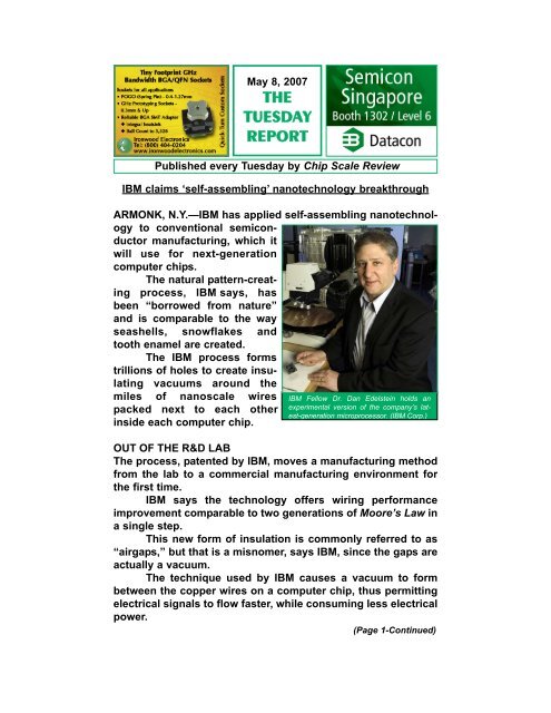
IBM Fellow Dr. Dan Edelstein holds an<br />
experimental version of <strong>the</strong> company’s latest-generation<br />
microprocessor. (IBM Corp.)<br />
OUT OF THE R&D LAB<br />
The process, patented by IBM, moves a manufacturing method<br />
from <strong>the</strong> lab to a commercial manufacturing environment for<br />
<strong>the</strong> first time.<br />
IBM says <strong>the</strong> technology offers wiring performance<br />
improvement comparable to two generations of Moore’s Law in<br />
a single step.<br />
This new form of insulation is commonly referred to as<br />
“airgaps,” but that is a misnomer, says IBM, since <strong>the</strong> gaps are<br />
actually a vacuum.<br />
The technique used by IBM causes a vacuum to form<br />
between <strong>the</strong> copper wires on a computer chip, thus permitting<br />
electrical signals to flow faster, while consuming less electrical<br />
power.<br />
(Page 1-Continued)
IBM claims nanotechnology breakthrough<br />
The self-assembly process enables <strong>the</strong> nanoscale patterning<br />
needed to form <strong>the</strong> gaps. The pattern, says IBM, “is<br />
considerably smaller than current lithographic techniques can<br />
achieve.”<br />
A vacuum is believed<br />
to be <strong>the</strong> ultimate insulator<br />
for wiring capacitance,<br />
which occurs when two conductors<br />
siphon electrical<br />
energy from one ano<strong>the</strong>r.<br />
This condition results in<br />
undesirable heat generation<br />
and reduces <strong>the</strong> speed that<br />
data can move through a<br />
semiconductor.<br />
Until now, IBM <strong>report</strong>s,<br />
chip designers were<br />
required to fight capacitance<br />
This microprocessor cross section shows empty<br />
space between <strong>the</strong> chip’s wiring. Vacuum gaps<br />
insulate <strong>the</strong> miles of nanoscale wire that connect<br />
hundreds of million of transistors. (IBM Corp.)<br />
issues by pushing more power through chips. Adding power,<br />
however, created many o<strong>the</strong>r problems.<br />
Designers have also employed insulators with improved<br />
insulating ability. These insulators, however, have become<br />
fragile as device features become smaller, and <strong>the</strong>ir insulating<br />
properties do not compare to those of a vacuum.<br />
A FIRST FOR TECHNOLOGY<br />
“This is <strong>the</strong> first time anyone has proven <strong>the</strong> ability to syn<strong>the</strong>size<br />
mass quantities of <strong>the</strong>se self-assembled polymers and<br />
integrate <strong>the</strong>m into an existing manufacturing process with<br />
great yield results,” <strong>report</strong>s Dr. Dan Edelstein, IBM Fellow and<br />
chief scientist for <strong>the</strong> self-assembly airgap project.<br />
IBM says <strong>the</strong> secret of its breakthrough resides in how<br />
IBM scientists moved <strong>the</strong> self-assembly process from <strong>the</strong> lab to<br />
a production manufacturing environment in a way that potentially<br />
yields million of chips with consistent, high-performance<br />
results.<br />
The method deployed to make airgaps by self-assembly<br />
eliminates <strong>the</strong> traditional masking and light-etching process.<br />
Instead, IBM scientists employ a mixture of compounds, which<br />
<strong>the</strong>y pour onto a silicon wafer with <strong>the</strong> wired chip patterns,<br />
before baking <strong>the</strong> wafer. [ibm.com]<br />
(Page 2)
Amkor chief operating officer to present conference keynote<br />
SAN JOSE—Oleg Khaykin, chief operating officer and executive<br />
vice president of Amkor Technology Inc., a leading provider<br />
of assembly and test services, will present <strong>the</strong> keynote speech<br />
at <strong>the</strong> International Wafer-Level Packaging Conference on<br />
September 18.<br />
His topic will be, “Packaging Trends and<br />
Solutions for Advanced Silicon Applications.”<br />
Khaykin was named to Amkor’s top operating<br />
post in January 2006, <strong>report</strong>ing to Chairman<br />
James Kim, and was vested with overall responsibility<br />
for worldwide sales, marketing, product business<br />
units, advanced product development, and<br />
manufacturing operations.<br />
Khaykin<br />
Khaykin joined Chandler, Ariz.-based Amkor in 2003 as<br />
executive vice president for corporate development and flipchip<br />
operations.<br />
SPEARHEADED AMKOR’S UNITIVE ACQUISITION<br />
He spearheaded Amkor’s 2004 acquisition of Unitive<br />
Electronics and <strong>the</strong> company’s strategic alliance with IBM.<br />
Prior to joining Amkor, Khaykin was vice president of<br />
strategy and business development for Conexant Systems<br />
Inc./Mind-speed Technologies from 1999-2003.<br />
He also served eight years with The Boston Consulting<br />
Group, where he worked with leading European and North<br />
American companies in <strong>the</strong> high tech, bio-technology, automotive,<br />
and aerospace industries.<br />
Khaykin holds an MBA from Northwestern University and<br />
a bachelor’s degree in electrical and computer engineering<br />
from Carnegie-Mellon University.<br />
The fourth annual IWLPC will be held from Sep. 17-19,<br />
with <strong>the</strong> first day devoted to workshops. Days 2 and 3 will<br />
include exhibits, panels, technical paper presentations and <strong>the</strong><br />
keynote dinner on Sep. 18 at <strong>the</strong> Wyndham Hotel in San Jose.<br />
The Conference is co-presented by <strong>Chip</strong> <strong>Scale</strong> <strong>Review</strong><br />
magazine and <strong>the</strong> SMTA, <strong>the</strong> nation’s leading electronics trade<br />
organization.<br />
A special “Early Bird” discount of 10 percent for attendees<br />
is available at <strong>the</strong> IWLPC website at smta.org/iwlpc.<br />
(Page 3)
People in <strong>the</strong> News<br />
Ang joins ASAT Holdings as VP of North American sales<br />
HONG KONG—Industry veteran Gabby Ang has joined ASAT<br />
Holdings Ltd. as vice president of North American sales, based<br />
in Milpitas, Calif.<br />
He <strong>report</strong>s to Joe Martin, executive vice<br />
president of sales and marketing.<br />
Most recently, Ang served as vice president<br />
of sales for Advanced Semiconductor<br />
Engineering, Taiwan. Earlier he served in sales<br />
positions with Advanced Interconnect<br />
Technologies, <strong>the</strong> packaging foundry recently<br />
acquired by Unisem.<br />
Gabby Ang Ang has also held sales positions with<br />
Amkor Technology Inc. and Interlek/Dynetics.<br />
He holds a master’s degree in international management<br />
and a bachelor’s degree in mechanical engineering. [asat.com]<br />
Indium Corp. announces management changes, promotions<br />
CLINTON, N.Y.—Indium Corp. of America has announced several<br />
management changes and promotions, including Ross<br />
Berntson, Scott Pringle and Jim Slattery.<br />
Berntson has been promoted to vice president of<br />
Indium’s Solder Products Business Unit. He most recently<br />
served as director of that unit.<br />
Pringle has been named sales director for global<br />
accounts, based in Sou<strong>the</strong>rn California. He has served as a<br />
consultant to Indium for two years.<br />
Slattery has been named vice president of technical service<br />
for Indium’s Metals & Chemicals Business Unit. He was<br />
most recently vice president of technical service for <strong>the</strong> Solder<br />
Products Business Unit. [indium.com]<br />
THE TUESDAY REPORT(TM)<br />
is published every Tuesday, except on federal and California state holidays,<br />
by <strong>Chip</strong> <strong>Scale</strong> <strong>Review</strong>. Copyright © Gene Selven & Associates Inc.,<br />
2007. All rights reserved. To contact <strong>the</strong> office of publication, phone<br />
408/996-7016.<br />
Publisher Gene Selven gselven@aol.com<br />
Editor Ron Iscoff chipscale@gmail.com<br />
Senior Editor Terrence E. Thompson tethompson@aol.com<br />
(Page 4)