Download Issue - Chip Scale Review
Download Issue - Chip Scale Review
Download Issue - Chip Scale Review
- No tags were found...

Create successful ePaper yourself
Turn your PDF publications into a flip-book with our unique Google optimized e-Paper software.
2<strong>Chip</strong> <strong>Scale</strong> <strong>Review</strong> March/April 2012 [<strong>Chip</strong><strong>Scale</strong><strong>Review</strong>.com]
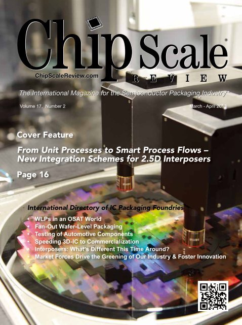
CONTENTSMarch April 2013Volume 17, Number 2<strong>Chip</strong> <strong>Scale</strong> <strong>Review</strong> March - April 2013 Volume 17, Number 2 <strong>Chip</strong><strong>Scale</strong><strong>Review</strong>.comVolume 17, Number 2 March - April 2013Cover FeatureFrom Unit Processes to Smart Process Flows –New Integration Schemes for 2.5D InterposersPage 16International Directory of IC Packaging Foundries• WLPs in an OSAT World• Fan-Out Wafer-Level Packaging• Testing of Automotive Components• Speeding 3D-IC to Commercialization• Interposers: What’s Different This Time Around?• Market Forces Drive the Greening of Our Industry & Foster InnovationThe International Magazine for Device and Wafer-level Test, Assembly, and PackagingAddressing High-density Interconnection of Microelectronic IC's including 3D packages, MEMS,MOEMS, RF/Wireless, Optoelectronic and Other Wafer-fabricated Devices for the 21st Century.FEATURE ARTICLESFrom Unit Processes to Smart Process Flows - New IntegrationSchemes for 2.5D InterposersThorsten Matthias, Markus Wimplinger, Paul Lindner, EV Group16The EVG IQ Aligner® is a 1X full-fieldexposure system optimized for 2.5D interposersbased on chip to-wafer integration. Thin filmprocessing of a thin wafer on a carrier beforeand after chip-to-wafer stacking, as well asafter over molding, are enabled by a number offeatures. The detailed process flow for a 2.5Dinterposer integration scheme is described inthe cover story. Photograph courtesy of EVGroup Europe & Asia/Pacific GmbHTesting of Automotive ComponentsDavide Appello, STMicroelectronicsWLPs in an OSAT World; The Top Ten OSAT WLP AssemblersSandra L. Winkler, New Venture Research2024PRESENTING THEEVOLUTION OF THEFLIP CHIP BUMPFrom the diverse solder bumpingsolutions of the last decade to thelarge scale production of today’sfine pitch copper pillar bumps,Amkor will provide a solution foryour packaging challenges.Amkor remains at the forefrontof semiconductor packagingdevelopment and performance.ELIMINATE THE GUESSWORKand talk to us today about our extensiveoffering of next generation design,assembly, and test solutions.visit amkor technology online for locations andto view the most current product information.www.amkor.com<strong>Chip</strong> <strong>Scale</strong> <strong>Review</strong> March/April 2013 [<strong>Chip</strong><strong>Scale</strong><strong>Review</strong>.com]1
FLIPCHIP BONDERBEST QUALITY, HIGHEST THROGHTPUT, FIELD PROOVEN RELIABILITY• Anti vibration design for high reliability• Best bonding accuracy by high performance of vision system• Flux residue inspection function at flux plate• Thin die bonding capability as thin as 50μmMODEL : FLIPCHIP BOND-A110■ SPECIFICATIONPRODUCTIVITY UPH ea 10,000PRECISION X-Y PLACEMENT μm ±6.0 @ 3σCHIP ROTATION θ ±0.1° @ 3σBONDING HEAD BONDING FORCE N 1 ~ 20(PROGRAMMABLE FROM 1N)UTILITIES MACHINE SIZE(W x D x H) mm 1,730 x 1,200 x 1,500MACHINE WEIGHT Kg 2,500Min. DIE SIZE mm 0.5 x 0.5THIN DIE HANDLING μm 502 <strong>Chip</strong> <strong>Scale</strong> <strong>Review</strong> Since March/April 1980 2013 [<strong>Chip</strong><strong>Scale</strong><strong>Review</strong>.com]#532-2, Gajwa-Dong, Seo-Gu, Incheon, 404-250, KoreaTEL : +82-32-571-9100 FAX : +82-32-571-9101www.hanmisemi.com
<strong>Chip</strong> <strong>Scale</strong> <strong>Review</strong> March/April 2013 [<strong>Chip</strong><strong>Scale</strong><strong>Review</strong>.com]3
JF MICROTECHNOLOGY SDN BHDBring Possibilities .\WeExplore thesenew exciting andoutstanding solutions onour website or with our nearestsales channel partner today.Find out more at:Or e-mail us at:4<strong>Chip</strong> <strong>Scale</strong> <strong>Review</strong> March/April 2013 [<strong>Chip</strong><strong>Scale</strong><strong>Review</strong>.com]
CONTENTSFEATURE ARTICLESFan-Out Wafer-Level Packaging: Extending the PlatformEoin O’Toole, NaniumMarket Forces Drive the Greening of Our Industry and Foster InnovationOsvaldo Gonzalez, CH2M HillDEPARTMENTSFrom the Publisher OSATS: Executives' PerspectivesKim Newman, <strong>Chip</strong> <strong>Scale</strong> <strong>Review</strong>Market Trends Interposers: What’s Different This Time Around?Linda C. Matthew, TechSearch International, Inc.Industry News<strong>Chip</strong> <strong>Scale</strong> <strong>Review</strong> StaffInternational Directory of IC Packaging FoundriesGuest Editorial Speeding 3D-IC to Commercialization: Update on SEMI StandardsJames Amano , SEMIProduct News<strong>Chip</strong> <strong>Scale</strong> <strong>Review</strong> StaffAdvertiser Index, Advertising Sales3642691127465456<strong>Chip</strong> <strong>Scale</strong> <strong>Review</strong> March/April 2013 [<strong>Chip</strong><strong>Scale</strong><strong>Review</strong>.com]5
Volume 17, Number 2The International Magazine for Device and Wafer-levelTest, Assembly, and Packaging AddressingHigh-density Interconnection of Microelectronic IC'sincluding 3D packages, MEMS, MOEMS,RF/Wireless, Optoelectronic and OtherWafer-fabricated Devices for the 21st Century.STAFFKim Newman Publisherknewman@chipscalereview.comLawrence Michaels Managing Directorlxm@chipscalereview.comDebra Vogler Senior Technical Editordvogler@chipscalereview.comDr. Thomas Di Stefano Contributing Editortom@centipedesystems.comJason Mirabito Contributing Legal Editormirabito@mintz.comPaul M. Sakamoto Contributing Editor Testpaul.sakamoto@comcast.netSandra Winkler Contributing Editorslwinkler@newventureresearch.comEDITORIAL ADVISORSDr. Andy Mackie (Chair) Indium CorporationRolf Aschenbrenner Fraunhofer InstituteDr. Thomas Di Stefano Centipede SystemsJoseph Fjelstad Verdant ElectronicsDr. Arun Gowda GE Global ResearchDr. John Lau Industrial Tech Research Institute (ITRI)Nick Leonardi Premier Semiconductor ServicesDr. Alan Rae Alfred Technology ResourcesDr. Ephraim Suhir ERS CompanyDr. Venky Sundaram Georgia Institute of Technology-3D Systems Packaging Research CenterFred Taber BiTS WorkshopFrancoise von Trapp 3D InCitesDr. C.P. Wong Georgia Institute of TechnologySUBSCRIPTION--INQUIRIES<strong>Chip</strong> <strong>Scale</strong> <strong>Review</strong>T 408-429-8585F 408-429-8605subs@chipscalereview.comAdvertising Production Inquiries:Kim Newmanknewman@chipscalereview.comCopyright © 2013 Haley Publishing Inc.<strong>Chip</strong> <strong>Scale</strong> <strong>Review</strong> (ISSN 1526-1344) is a registered trademark ofHaley Publishing Inc. All rights reserved.Subscriptions in the U.S. are available without charge to qualifiedindividuals in the electronics industry. Subscriptions outside of theU.S. (6 issues) by airmail are $100 per year to Canada or $115 peryear to other countries. In the U.S. subscriptions by first class mailare $95 per year.<strong>Chip</strong> <strong>Scale</strong> <strong>Review</strong>, (ISSN 1526-1344), is published six times ayear with issues in January-February, March-April, May-June, July-August, September-October and November-December. Periodicalpostage paid at Los Angeles, Calif., and additional offices.POSTMASTER: Send address changes to <strong>Chip</strong> <strong>Scale</strong> <strong>Review</strong>magazine, P.O. Box 9522, San Jose, CA 95157-0522Printed in the United StatesFROM THE PUBLISHERToday’s OSATS (Outsourced Semiconductor Assembly and TestServices) leaders are capable of delivering innovative solutions tointegrated device manufacturers in every segment of the supply chain.These services include comprehensive support for package design,wafer bumping, probing, sorting, thinning, dicing, wire and flip-chip bonding, 3D/stacked packaging, package-in-package (PiP) and package-on package (PoP). Inthe following commentary, I wanted to offer recent viewpoints directly from thetop management of the OSATS providers. The following executive commentsare recently extracted from their respective quarterly and annual reports to theirshareholders.Ken Joyce, Amkor's President & CEO noted the following in his report: “Lookingahead to the first quarter 2013, we are seeing seasonal demand patterns and we arecurrently planning capital additions of around $450 million for 2013 primarily tosupport the growth opportunities we see in mobile communications.ASE Group Chairman and CEO Jason Chang noted in his company’s report that“ASE's continued execution to expand operations and deliver growth resulted insetting a new record for the company in 2012 particularly as we embrace this era ofmobile communications and optimize our business activities accordingly.” Changadded, "The macroeconomic climate and the cyclic nature of our industry willalways impact our bottom line, however, our global strategy – expanding regionalcapabilities, manufacturing capacity, and product portfolio – is proving the rightlong-term strategy for our ongoing success. Clearly, semiconductor is at the center ofhuge technology transitions worldwide.”Tan Lay Koon, President & CEO of STATS <strong>Chip</strong>PAC, commented in part,“Based on current visibility, we expect net revenues in the first quarter of 2013 to bedecreased compared to the prior quarter as the revenue outlook for first quarter of2013 is impacted by seasonality.”John Chia Sin Tet, Group Managing Director of Unisem (M) Berhad, commentingin the company's report said, “The operating environment remains challenging dueto global economic uncertainties. We expect a soft first quarter due to continuedinventory adjustments in the industry.”In this issue, we cover the top ten OSATS WLP assemblers, fan-out wafer-levelpackaging, new integration schemes for 2.5D interposers, as well as what’s differentthis time around in a market outlook for interposers, and how the industry canleverage SEMI standards to speed 3D-IC to commercialization and finally, we roundout the issue with articles that discuss the market forces that are driving the greeningof our industry while fostering innovation and the testing of automotive components.Once again, CSR delivers the pertinent and carefully crafted articles to provideour readers the foundation to maintain a solid understanding of current trends andtechnologies, whether in-house or outsourced.Kim NewmanPublisherOSATS: Executives’ Perspectives6<strong>Chip</strong> <strong>Scale</strong> <strong>Review</strong> March/April 2013 [<strong>Chip</strong><strong>Scale</strong><strong>Review</strong>.com]
“Panasonic equipmentdelivers best-in-classaccuracy and PanaCIM ®drives operational efficiency”“ Panasonic equipment delivers the best-in-classaccuracy, repeatability, and dependability neededto manufacture the high-quality products ourcustomers expect.PanaCIM software drives operational effi ciencythroughout our high-mix, low-to-medium-volumeprocess—from quick changeovers to real-timeproduction monitoring and reduced rework.Selecting Panasonic has helped us to keepoverall manufacturing costs down, maintainour competitiveness, and allow us to passcost savings to our customers.”Dave SpeharDirector of OperationsAs a manufacturer, Panasonic understands the evolvingdemands of today’s electronics assembly manufacturingenvironment. And that uniquely enables us to provide scalable,integrated, and effi cient solutions that help our customersremain viable in a competitive market.No matter if you’re high mix/low volume, low mix/high volume,or anything in between, Panasonic equipment, MES software,and other services can help improve throughput and effi ciencywhile keeping quality reliably high.Add value, add sustainability, add Panasonic.For more information, visit www.panasonicfa.com/pennatronics<strong>Chip</strong> <strong>Scale</strong> <strong>Review</strong> © March/April 2013 Panasonic Corporation 2013 [<strong>Chip</strong><strong>Scale</strong><strong>Review</strong>.com]of North America. All rights reserved. 7
8<strong>Chip</strong> <strong>Scale</strong> <strong>Review</strong> March/April 2013 [<strong>Chip</strong><strong>Scale</strong><strong>Review</strong>.com]
MARKET TRENDSInterposers: What’s Different This Time Around?By Linda C. Matthew [TechSearch International, Inc.]Silicon interposers are atechnology with a historyof multiple incarnationsover more than 20 years. Today,interposers with TSVs are consideredan alternative to 3D IC structures wherethe die are stacked on top of eachother using TSVs. Applications forinterposers with TSVs include ASICsfor networking applications and FPGAs.Some companies are also examining thepotential for interposers with GPU/CPUand mobile computing. The drivers aremainly partitioning large die, integratingsingle chips into a module, reducingdie size where substrate density is theconstraint, and minimizing the stresson large die that are fabricated withextra-low-k (ELK) dielectrics. Mostof today’s interposers are silicon, butresearch is also underway on glassinterposers. Some companies are eveninvestigating the possibility of laminatesubstrates as interposers.Old vs. New Interposers: A HistoryLessonOne question that sometimes arisesis how today’s silicon interposers differfrom the thin-film on silicon (MCM-D)of the past. Through most of the 1990s,silicon substrate work was underway atvarious companies as part of the multichipmodule (MCM) movement. Thinfilm-on-siliconMCM-D, where D stoodfor "deposited," was one substrate choicecompeting with laminate (MCM-L)and ceramic (MCM-C) substrates. Thebenefits of silicon would have combinedto give a denser, higher-performancemodule than laminate substrates could.But ultimately, the technology did notpenetrate the high-volume commercialmarket and lost the battle to conventionalFR-4 because of cost and logistics. Thecompeting laminate substrates were lessdense because of the rough topography ofthe FR-4, but had much lower cost. Andfrom a logistics standpoint, the higherdensity of the silicon substrate could notbe fully utilized because the large numberof high lead-count die that it could supportcreated a package that was extremelydifficult to test and had low yields. Atechnology that could not find a largemarket in 1995 is generating a differentresponse today because packaging andintegration have evolved substantially.Advantages of Silicon InterposersThe interposers in production today aresilicon with redistribution layers on eachside. Today, multiple chips are mountedside-by-side on the interposer, but futureversions show the possibility of stackeddie with TSVs mounted on the interposer.Most of today’s interposers are passivestructures, but the incorporation ofpassives has been demonstrated.The advantages of 2.5D (dieconnected to silicon interposers withTSVs) result from the combinationof the silicon material properties andmulti-chip packaging. Advantagesinclude: 1) High wiring density due tothe very flat substrate; 2) Efficiency ofwiring layers on each chip because theglobal wiring is on the interposer; 3)Efficiency of active area on each chipbecause there is no keep-out area forthe TSV; 4) TCE matched to the silicondie; 5) Lower cost of active devices dueto partitioning large die with improvedperformance; 6) Lower cost of activedevices due to smaller flip-chip bumppitch; 7) Lower power requirementsthan equivalent single-chip packagesdue to multiple chips combined on onesubstrate; 8) Possibility of integratingpassives into the substrate; and 9) Moreefficient heat dissipation than a 3D stackusing a thermal lid.Silicon Interposer: Planned and inProductionSilicon interposers are used as LEDsub-mounts, substrates with integratedpassives for transceiver/receiverapplications, substrates for multichipmodules, and interposers withthrough-silicon vias will increasinglybe used for 2.5D applications. Networksystem and server makers, includingCisco, Ericsson, Fujitsu, Huawei, IBM,and Juniper Networks, show siliconinterposers on their product roadmaps.Silicon interposers are used for RFmodules, where they offer the benefitof integrated passives. NXP's spinoff,IPDiA, manufactures siliconinterposers for RF modules andhundreds of millions of units have beenproduced. STMicroelectronics hasinternal production on thin-film-on-glassand thin-film-on-silicon and producestransceiver/receiver modules internally.STATS <strong>Chip</strong>PAC supplies siliconinterposers with integrated passives forRF module applications; the companydescribed some of its developments insilicon interposers using Cu pillar andAgSn micro bumps for silicon interposerapplications [1]. Test chips with a 5mm x5mm outline were fabricated with 10,000micro bumps on a 40 or 50µm pitch.IBM's work with silicon interposersdates back to the late 1980s. Recently,the company has developed multipletechnologies for TSV applications,including a program to fabricatesilicon interposers. IBM has evaluatedthe thermal cycling reliability of<strong>Chip</strong> <strong>Scale</strong> <strong>Review</strong> March/April 2013 [<strong>Chip</strong><strong>Scale</strong><strong>Review</strong>.com]9
low-volume solder joints for theconfiguration of a silicon chip onsilicon interposer on organic substrate[2]. Results show that the significantCTE mismatch between the silicon andorganic substrate causes large stresses inthe low volume solder joints.IBM supplies a silicon interposerwith TSVs to Semtech Corporationfor a mixed signal application. Themodule integrates a high-performancedata converter with a DSP andincludes deep trench capacitors in theinterposer. The interposer enablesmixed IC technologies and solvesdensity, power, and bandwidth issues.Applications include receivers forfiber optic telecommunications, highperformanceRF sampling and filtering,test equipment and instrumentation, andsub-array processing for phased arrayradar systems.IBM has also described its workon a silicon interposer in an opticaltransceiver module [3]. This is thefirst demonstration of the Terabusoptoelectronic (OE) module using aTSV silicon interposer for the dense 24TX + 24 RX transceiver. The interposerenables integration of CMOS andoptoelectronic devices. It supports fourflip-chip devices: two optoelectronicarrays (VCSELs and photodiodes) andtwo CMOS ICs with receivers andlaser drivers. IBM refers to the entireinterposer sub-assembly as an Optochip.Xilinx’s Virtex-7 2000T FieldProgrammable Gate Array (FPGA) usesa silicon interposer with TSVs. Xilinxreports that the 2000T is the world’shighest-capacity FPGA, using 6.8billion transistors, 2 million logic cells,and the equivalent of 20 million ASICgates for system integration, ASICreplacement, and ASIC prototyping andemulation. The key to the performancegains is the partitioning of an FPGAdie into four “slices” that are mountedon a silicon interposer or what Xilinxcalls its “Stacked Silicon Interconnect”technology. Using internal designcapability, Xilinx has been able topartition its die into slices that aresmaller than a conventional large FPGAdie. The slices are fabricated in 28nmsilicon technology. TSMC fabricatesthe passive silicon interposer in 65nmnode silicon technology. TSVs in theinterposer have an aspect ratio of 10:1.In March 2012, Altera and TSMCjointly announced the world's firstheterogeneous 3D-IC test vehiclemanufactured with TSMC's <strong>Chip</strong>-on-Wafer-on-Substrate (CoWoS) process[4]. CoWoS is TSMC's entry into thecontract assembly world, and uses chipon-waferbonding to assemble die toa silicon interposer. The interposer isthen attached to the substrate to formthe final component. By attaching thedevice silicon to the thick interposerbefore it finishes fabrication, the processavoids manufacturing-induced warping.SuppliersSilicon interposer research activities,prototype development, and shipmentsare taking place at a number ofcompanies including ALLVIA, ASE,Dai Nippon Printing, Ibiden, IBM, IMT,IPDiA (formerly NXP), NEPES, ShinkoElectric, Silex Microsystems, SPIL,STATS <strong>Chip</strong>PAC, Teledyne Dalsa,Tezarron and its Novati subsidiary(formerly SVTC’s Austin, Texasfacility), TSMC, and UMC. Figure 1shows the chip-to-chip (C2C) assemblywith Tezzaron’s interposer on thebottom; the interposer was developedwith IME in Singapore. While manycompanies have contemplated the designFigure 1: C2C with Tezzaron’s interposer on thebottom. SOURCES: Tezzaron, IMEof structures with silicon interposers,the industry infrastructure and supplybase for the widespread adoption of thetechnology has been a concern. TheTable 1 shows specifications of siliconinterposers under evaluation.PropertyValueSubstrate length, width (mm) 5.5 - 55Substrate thickness (μm) 100 - 250, 400Via metalCuRDL (number of layers) 1 - 5Via diameter (μm) 10 - 75Via pitch (μm) 35 - 200Table 1: Specifications of silicon interposers underevaluation. Source: TechSearch International, Inc.References1. S.W.Yoon, D. Shariff, J.H.Ku, P.C. Marimuthum, F.Carson, "3D TSV InterposerTechnology with Cu/SnAgMicrobump Interconnection," 6thInternational IMAPS Conferenceand Exhibition on DevicePackaging, March 2010.2. K. Sakuma, K. Sueoka, S. Kohara,K. Matsumoto, H. Noma, T.Aoki, et al., "IMC Bonding for3D Interconnection," ElectronicComponents and TechnologyConference, June 2010, pp. 864-871.3. F. Doany, B. Lee, C. Schow, C.Tsang, C. Baks, Y. Kwark, etal., "Terabit/s-Class 24-ChannelBidirectional Optical TransceiverModule Based on TSV Si Carrierfor Board-Level Interconnects,"Electronic Components andTechnology Conference, June2010, pp. 58-65.4. "Altera and TSMC JointlyDevelop World's First 3D ICHeterogeneous Test VehicleUsing CoWoS Process," AlteraPress Release, March 22, 2012.BiographyLinda C. Matthew received her BSand MS degrees in materials science andengineering from MIT; she is a SeniorAnalyst at TechSearch International,Inc.; email tsi@techsearchinc.com10<strong>Chip</strong> <strong>Scale</strong> <strong>Review</strong> March/April 2013 [<strong>Chip</strong><strong>Scale</strong><strong>Review</strong>.com]
INDUSTRY NEWSImec and Qualcomm Extend R&DCollaborationImec and Qualcomm Technologies,Inc., a wholly owned subsidiary ofQualcomm Incorporated, announcedan extended collaboration agreement toaccelerate scaling technologies for logicand memory devices. The first fablessintegrated circuit company to becomea core partner of imec, QualcommTechnologies will gain comprehensiveinsight into all advanced processtechnologies under investigation at imecto help shape future product roadmaps.By gaining early information on CMOSadvancements, the product designcommunity in IDMs, fabless, fabliteand system-design companies canbetter anticipate the future impact andpotential of new technologies to shapedevelopment efforts.“We have collaborated with imecon the 3D stacking program for thelast four years and we look forward toexpanding our engagement with imecto include CMOS research and the newMRAM program,” said Jim Thompson,EVP, Engineering at QualcommTechnologies Inc. “Early engagement onnew microelectronic technologies withimec enables Qualcomm to deepen theco-optimization of product architectureand technology while mitigating newtechnology risk in collaboration withour supply partners.”Leti Targets European SiliconPhotonics Supply ChainCEA-Leti has announced that it willcoordinate a four-year project aimedat building a European-based supplychain in silicon photonics and speedingindustrialization of the technology.The PLAT4M (Photonic LibrariesAnd Technology for Manufacturing)project will focus on bringing theexisting silicon photonics researchplatform to a level that enables seamlesstransition to industry, suitable fordifferent application fields and levels ofproduction volume.PLAT4M, which is funded by aEuropean Commission grant of 10.2million euros, includes 15 leadingEuropean R&D institutes and CMOScompanies, key industrial and researchorganizations in design and packaging,as well as end users in differentapplication fields to build the completesupply chain.“Silicon with its mature integrationplatform has brought electronic circuitsto mass-market applications – ourvision is that silicon photonics willfollow this evolution,” said LaurentFulbert, Integrated Photonics ProgramManager at CEA-Leti, coordinatorof PLAT4M. “Upgrading existingplatforms to become compatible withindustrialization is now essential andthis requires streamlining and stabilizingthe design and process flows by takinginto account design robustness, processvariability and integration constraints.The PLAT4M partners bring a criticalcombination of expertise to thechallenge of building a complete supplychain for commercializing siliconphotonics in Europe.”According to CEA-Leti, a surge inoutput of silicon photonics research inrecent years has significantly boosted thepotential for commercial exploitation ofthe technology. However, most of thisR&D has been devoted to developingelementary building blocks, rather thanfabricating complete photonic integratedcircuits that are needed to support largepotential markets.CEA-Leti further announced thatthe PLAT4M consortium will maketechnologies and tools mature bybuilding a coherent design flow,demonstrating manufacturabilityof elementary devices and processintegration and developing a packagingtoolkit. The project will validatethe complete supply chain throughapplication-driven test vehiclesrepresenting various application fields,such as telecom and datacom, gassensing and light detection and ranging(LiDAR) and vibrometry. It also willfocus on preparing the next-generationplatform by setting up a roadmap forperformance evolution and assessingscalability to high-volume production.The supply chain will be based ontechnology platforms of Leti, imecand STMicroelectronics, supportedby a unified design environment. Theproject is expected to have multiplebenefits for the European photonicindustry including:1) Preparing the supply chain for siliconphotonics technology, from chipleveltechnology to packaged circuits;2) Making integration technologiesaccessible to a broad circle of users ina fabless model; 3) Contributing to thedevelopment of a design environmentthat facilitates photonics/electronicsconvergence; 4) Moving the emphasisfrom the component to the architecture,and thus concentrate efforts on newproducts or new functionalitiesrather than the technology level; 5)Aggregating competencies in photonics/electronics design and fabrication;and 6) Retaining the key added valuein components in Europe throughoptoelectronic integration, with littleadded value in offshore assembly.Among the members of theconsortium, in addition to CEA-Leti,are: imec, the University of Paris-Sud,III-V Lab, TNO, Mentor Graphics,PhoeniX BV, Si2, STMicroelectronics,Tyndall-UCC, Aifotec, Polytec, ThalesResearch & Technology, and NXP.Yole: BioMEMS Market to AlmostTriple in Size Over Next 5 YearsYole Développement released itslatest market forecast for BioMEMS.According to the market analysis andresearch firm, the BioMEMS market isexpected to grow rapidly, from $1.9B in2012 to $6.6B in 2018 (Figure 1). Thisgrowth is almost a tripling in size, withmobile care applications contributingsignificantly.Benjamin Roussel, Technology &<strong>Chip</strong> <strong>Scale</strong> <strong>Review</strong> March/April 2013 [<strong>Chip</strong><strong>Scale</strong><strong>Review</strong>.com]11
$MBioMEMS and microsystems for life science market (in $M)Including: pressure sensors, silicon microphones, accelerometers, gyroscopes, optical MEMS and image sensors, microfluidic chips,microdispensers for drug delivery, flow meters, infrared temperature sensors, emerging MEMS (RFID, strain sensors, energy harvesting)70006000500040003000200010000(Source: BIOMEMS report, Yole Développement, February 2013)2011 2012 2013 2014 2015 2016 2017 2018© February 2013Figure 1: BioMEMS and Microsystems for Life Science Market (in $M). SOURCE: Yole Développement.Market Analyst at Yole, also pointedout that microsystems integration is fastbecoming a key added-value for systemmanufacturers.Microsystem devices have becomeincreasingly visible in the healthcaremarket by serving as solutionsadapted to the requirements of variousapplications. The usefulness of thesedevices is two-fold: for one, theyimprove medical device performancefor the patient; and secondly, theyoffer competitive advantages tosystem manufacturers. For example,the introduction of accelerometers inpacemakers has revolutionized thetreatment of cardiac diseases.In related news, Yole also releaseddata crediting STMicroelectronics forcapitalizing on the booming demand forMEMS in mobile devices by shipping58% more MEMS units in 2012 to12<strong>Chip</strong> <strong>Scale</strong> <strong>Review</strong> March/April 2013 [<strong>Chip</strong><strong>Scale</strong><strong>Review</strong>.com]
incorporation into a PGS commercialstreamer system to acquire more preciseseismic data during seismic surveys tolocate and estimate the size of offshoreoil and gas reserves.Figure 2: 2010-2012 MEMS Revenue Evolution for Top 3 MEMS Companies. SOURCE:Yole Développementbecome the first company to reach $1billion in MEMS sales (Figure 2). Thatwas in a year when the average pricesof accelerometers and gyroscopes thatare its core MEMS products dropped by20%-30%, noted the research firm.“The company [STMicroelectronics]was there and ready with its 8-inch fabwhen the volume demand started, aswell as a large portfolio of productsand low prices,” said Laurent Robin,Activity Leader, Inertial MEMS Devices& Technologies at Yole Développement.“They could use a feed-the-fab-strategyto build volumes, and discounts forbuyers of multiple devices, to meetthe price demands of the cell phonemakers.”sea seismic oil and gas exploration.The collaboration leverages IME’sexperience in designing highperformanceMEMS sensors, MEMSprocess platforms and in-housepackaging capabilities, and PGS’sexpertise in seismic exploration. Theproject will demonstrate a MEMSsensor and provide guidelines for thepackaging and integration with ASIC inthe next phase.The MEMS sensor is targeted forESCATEC Celebrates Ten Years ofOperation at Its Heerbrugg FactoryESCATEC is celebrating the tenthanniversary of the opening of itsHeerbrugg facility (Figure 3) with aspecial event for customers. "The themeof our event is Building Bridges,"explained Christophe Albin, ExecutiveChairman of the Board of Directors andfounder of ESCATEC. "Heerbrugg'scentral European location in Switzerlandenables ESCATEC to build bridges forrapid communication and support forour customers all over the EU. FromHeerbrugg we provide contract productdesign services and manufacturing fromprototypes to low volume, high mixassembly. We also act as a bridge toour factories in Asia that combine ourSwiss quality and reliability standardswith low labor costs for high-volumeproduction."Yole: Flip-<strong>Chip</strong> MarketReinvigorated by Cu Pillar andMicro-BumpingYole Développement projects thatover the next five years, a 3x waferA*STAR’s IME’s LatestCollaboration Leverages PackagingCapabilityA*STAR’s Institute ofMicroelectronics has signed anagreement to collaborate with PetroleumGeo-Services (OSE:PGS), a focusedgeophysical company headquarteredin Oslo, Norway, to develop a highperformance microelectromechanicalsystems (MEMS) based sensor for deepFigure 3: ESCATEC’s Heerbrugg Factory.<strong>Chip</strong> <strong>Scale</strong> <strong>Review</strong> March/April 2013 [<strong>Chip</strong><strong>Scale</strong><strong>Review</strong>.com]13
growth is expected for the flip-chipplatform, reaching 40M+ of 12’’eq wspyby 2018. Despite its high 19% CAGR,flip-chip is not a new technology, notedthe marketing consulting firm — havingbeen first introduced by IBM over 30years ago. Flip-chip is keeping up withthe times and new bumping solutionsare being developed to serve the mostadvanced technologies, like 3DICand 2.5D.Yole further observed that in 2012,bumping technologies accounted for81% of the total installed capacity inthe middle end area, representing 14M+12’’eq wafers — and fab loading ratesare high as well, especially for the Cupillar platform (88%).Yole also reported that in 2012, flipchipwas a $20B market (making itthe biggest market in the middle-endarea), and the research firm expectsit to continue growing at a 9% clip,ultimately reaching $35B by 2018. Flipchipcapacity is expected to grow overthe next five years to meet large demandfrom three main areas: 1) CMOS 28nmIC, including new applications like APEand BB; 2) The next-generation of DDRMemory; and 3) 3DIC/2.5D interposerusing micro-bumping. Driven by theseapplications, Cu pillar is on its way tobecoming the interconnect of choice forflip-chip.Peter Chiang Joins IPC as VP of IPCChinaIPC announced the appointment ofPeter Chiang as its new Vice Presidentof IPC China. He will also serve asIPC’s chief representative for Taiwan.Within his role of VP of IPC China,Chiang will work in conjunction withIPC China President Phil Carmichael tolead the organization’s China operationsand staff. As chief representative forTaiwan, he will have responsibilityfor providing standards developmentactivity support, raising awareness ofIPC and its programs, making companyvisits and establishing relationships withprospective distributors in the region.“Peter is an experienced businessprofessional with more than two decadesexperience in sales and marketing,training, finance, and management andservice to multi-national companies,”says Phil Carmichael, president, IPCChina. “His market analysis skills andproven performance record of stellarclient service made him the idealcandidate to work with IPC Chinastaff to build IPC’s presence in China,increase Taiwanese OEM membershipand assist IPC members in achievingtheir business goals.”Prior to IPC, Chiang held keypositions at Lexmark Asia Pacific Corp.,Silicon Graphics/CRAY RESEARCH,Wang Industrial Co. Ltd., and ChinaManagement System Corporation. Heholds a Bachelor of Science degreein computer science from NationalTaipei Commercial College in Taiwanand is fluent in Mandarin, English andTaiwanese. He works from IPC’s Chinaheadquarters office in ShanghaiTriton Micro Technologies toDevelop Via-Fill TechnologyTokyo-based Asahi Glass Co., Ltd.(AGC) and nMode Solutions Inc.of Tucson, Arizona, have invested$2.1 million to co-found a subsidiarybusiness, called Triton MicroTechnologies (www.tritonmicrotech.com), to develop via-fill technology forinterposers, enabling next-generationsemiconductor packaging solutionsusing ultra-thin glass. The newcompany, headquartered in Tucsonwith a manufacturing facility plannedin California, will combine nMode’sinterposer technology for electricallyconnecting semiconductor devices withAGC’s materials technology and microholedrilling techniques to produce2.5-dimensional (2.5D) and threedimensional(3D) through-glass-via(TGV) interposers needed for advancedsemiconductor devices.To achieve the next-generation inhigh-density semiconductor packaging,interposer technologies are neededto form the high number of electricalconnections between a silicon chipand a printed circuit board. Interposersallow high packaging integration in thesmallest available form factors.Triton Micro Technologies willmanufacture ultra-thin glass interposersusing a high-efficiency continuousprocess that lowers costs and helps tocommercialize the widespread use ofinterposers. The company will drawupon nMode’s intellectual property andAGC’s proven carrier-glass technologyand via-hole drilling methodologiesto fabricate its interposers. Triton thenwill apply its proprietary technologyto fill the high-aspect-ratio via holeswith a copper paste that has the samecoefficient of thermal expansion asglass. This reduces the potentiallydamaging effects of thermal stressduring manufacturing and long-termuse. Triton’s process creates highqualityelectrodes within the interposerto provide the electrical interfacecapable of accommodating advanced,high-density ICs.Triton’s interposers are compatiblewith wafers having diameters from100mm to 300mm and thicknesses of0.7mm and below. The company alsocan design and manufacture customizedsolutions for unique applications.“The global semiconductor industryrecognizes that silicon is approachingits performance limits as an interposermaterial, but the need remains tocreate smaller, more efficient packagesfor today’s and tomorrow’s highperformanceICs,” said Tim Mobley,CEO at Triton. “Our technology allowsus to achieve known-good-die testingat the highest levels of packagingintegration, faster cycle times and thelowest cost per unit in the market.”Here We Come!The premier international packaging,components, and microelectronicssystems technology conference, theElectronic Components and TechnologyConference (ECTC), will be upon us14<strong>Chip</strong> <strong>Scale</strong> <strong>Review</strong> March/April 2013 [<strong>Chip</strong><strong>Scale</strong><strong>Review</strong>.com]
shortly. The 63rd ECTC will be heldat the Cosmopolitan of Las Vegas, LasVegas, Nevada, USA from May 28 -May 31, 2013.This year’s conference will haveabout 40 technical sessions (oralpresentations, interactive presentations,and student posters), 16 professionaldevelopment courses, a paneldiscussion, a plenary session, a CPMTSeminar, and a technology corner forexhibitors. The line-up of sessionsincludes: Advanced Packaging,Electronic Components & RF, EmergingTechnologies, Interconnections,Assembly & Manufacturing Technology,Materials & Processing, Modeling& Simulation, Optoelectronics, andApplied Reliability.Much can be learned at this annualconference. Information on two of thetopics covered at the conference ispresented below.Through-Via InterconnectionThe topic of through silicon vias(TSVs) incorporates both 2.5-D and 3-Dtechnology. 3-D interconnection involvesstacking ICs vertically, and routingeach of the die to the substrate belowby incorporating vias that go throughthe bulk silicon of the die beneath it tocarry the electrical signal to the substratebelow. In 2.5-D, chips are partitioned andplaced side by side on an interposer withthrough-vias to a substrate below.The identified potential markets forthrough-via technology have a combinedunit potential of 39 billion units, whichwill expand to 60 billion units in 2016.The forecast for through-via technology isfor this new technology to be less than 1%of the total available identified marketsthrough 2016, but growing each year.Fan-Out or Reconfigured WLPReconfigured or fan-out waferlevelpackages were introduced in2006. After devices are manufacturedon a wafer, the devices are sawn andtransferred on a carrier to anotherlarger wafer that has gaps betweendie, which are filled with over moldmaterial that also coats the back side ofthe devices for protection. This allowsfor a larger surface on which to extenda redistribution layer, thus allowing forfar more I/Os than would be possible onthe original smaller surface. Solder ballsor bumps can be added to this surfacefor interconnection to a printed circuitboard.Units of fan-out WLPs are growingat a CAGR of 11.6% for the years 2011through 2016. These packages arebetween 8 and 9% of the total WLPpopulation output.<strong>Chip</strong> <strong>Scale</strong> <strong>Review</strong> March/April 2013 [<strong>Chip</strong><strong>Scale</strong><strong>Review</strong>.com]15
From Unit Processes to Smart Process Flows –New Integration Schemes for 2.5D InterposersBy Thorsten Matthias, Markus Wimplinger, Paul Lindner [EV Group]Ahot topic in the packagingworld right now is the2.5D interposer. Aninterposer allows inter-chipcommunication between multiple chipswith intra-chip interconnects, therebyenabling unmatched bandwidth, reducedpower consumption, and very goodheat spreading. Interposers also enablea modular design and manufacturingarchitecture by die partitioning.Finally, 2.5D interposers allow theimplementation of a large part of thepromise of 3D ICs without the need tomake through-silicon vias (TSVs) intothe chips.While the technical attractiveness ofinterposers has been acknowledged bythe industry, cost is still prohibitive formany applications. At the IEEE GlobalInterposer Technology (GIT) Workshopin November 2012, a cost target of 1cent/mm² for consumer electronic applicationswas discussed. Interposer dies are verylarge, which results in a large cut-off area.Assuming that 80% of the wafer can beused for manufacturing, the 1cent/mm²equates to $543USD/wafer total cost-ofownership,which is an ambitious target.There are multiple approaches toreduce the cost of interposers. Figure 1shows the basic concept of an interposerwith RDL (redistribution layer) andmicrobumps on one side, TSVs throughthe interposer, and C4 bumps on theother side. One cost reduction approachis to replace the single crystal siliconwafer by cheaper materials like glassor polycrystalline silicon. Anotherapproach is to reduce manufacturing costFigure 1: Schematic cross section of a 2.5Dinterposer: C4 bumps on the bottom side,microbumps on the top side of theinterposer; multiple redistribution layers(RDL) on top and bottom side.by increasing substrate size: LCD sizepanels for glass and poly-Si, and 450mmwafers for single-crystalline silicon.Lithography is another important area.The established patterning technologiesfrom laminates are probably notsufficient for many applications, whereasfront end lithography with line/spacedimensions of 1µm/1µm is probably notnecessary for many applications. There isa trade-off between resolution and cost.At the GIT Workshop, several speakersopined that 3-4µm L/S might be thesweet spot enabling high performanceinterposers at a reasonable price.Via manufacturing, however, is alsoa significant cost contributor. From theelectrical performance point of view,10x100 vias seem sufficient for manyapplications. However, via manufacturingcosts are positively correlated with thevia depth and the via aspect ratio. Thecost for creating a 10x100 via is morethan twice the cost for a 10x50 via, whichagain costs more than twice as much asa 10x25 via. So from the cost reductionpoint of view, it would make sense toreduce the interposer thickness. Theproblem is that reducing the interposerthickness magnifies the problems withdie handling and assembly. In theremainder of the article we will discusshow thin interposer handling can beavoided by smart process integration.Interposer Manufacturing FlowsUp until now, interposer manufacturingflows have been envisioned as follows:the interposer die, as well as the diesto be stacked on the interposer, areindividually manufactured (front-andbackside of the thin dies including bumpson both sides). In the end, the thin diesare stacked on the thin interposer. Thisprocess flow allows that both active dies,as well as the interposer, can be testedprior to stacking. More important, it fitsthe established manufacturing supplychain, where foundries would producethe interposer wafer and OSATs wouldtake care of chip stacking, assemblyand packaging. While this processsequence intuitively seems an obviouschoice, it creates many difficulties fromthe manufacturing point of view, asdelineated below.a) Bow and warpage of the thininterposer is a serious issue.While thin-wafer processing iswell established by the usage ofa temporary carrier, there is nogood solution for handling ofthin dies, especially if bumps arealready on both sides. Not onlyare the thin dies fragile, but theinternal stress creates die bowand warpage, which magnifiesthe difficulties. A die, which isflat at room temperature, mostlikely will be bent at elevatedtemperature. Precision alignmentand bonding are difficult undersuch circumstances.b) The dies are bonded to theinterposer with microbumpsand a thermo-compressionbond process. For high-densityTSV applications, a solder-lessbonding approach like Cu-Cubonding might be necessary. Thethermo-compression bond processprefers elevated temperatures upto 350°C. But if C4 bumps arealready on the other side of theinterposer die, then the thermocompressionbond temperaturehas to be reduced in order not tomelt the C4 bumps. This results inreduced bond contact quality andincreased cycle time.c) Thermo-compression bondingrequires quite high bond forces ofseveral hundred Newtons per die.The C4 bumps on the bottom side16<strong>Chip</strong> <strong>Scale</strong> <strong>Review</strong> March/April 2013 [<strong>Chip</strong><strong>Scale</strong><strong>Review</strong>.com]
of the interposer are spherical,which means that they formpoint contacts to a planar surface,which would result in immediatedeformation of the bumps.A New Process FlowBreaking with the goal of stackingcompletely processed thin dies allowsthe creation of easier, smarter and moreelegant process flows. One potentialprocess flow for 2.5D interposers (EVGpatent pending) with C4 bumps on thefrontside, microbumps on the backside,and multiple RDL layers, would beas follows (Figure 2 shows the entireprocess flow):Manufacturing of Thin InterposerWafer. The interposer wafer afterfrontside processing is temporarilybonded to a carrier wafer for thinningand backside processing (Figure 2). Therecent advances in thin-wafer processingby temporary bonding and debondinghave been reviewed in the literature [1].Within this process flow, “frontside”of the interposer refers to the side withC4 bumps. These C4 bumps could becreated prior to temporary bonding or ata later point in the manufacturing line(bump-last processes).<strong>Chip</strong>-to-wafer Integration. Multiplechips are stacked onto the interposer nextto each other. Note that one chip itselfcould be a 3D stack, e.g., a memorycube. The entire chip stacking happenswhile the thin interposer wafer is stillbonded to the carrier wafer (Figure3). This has the advantage that thecarrier wafer compensates and absorbsall the internal stress and keeps theinterposer wafer flat. In the case wherethe C4 bumps are already present on thefrontside of the interposer, they are safelyembedded in the adhesive. It is importantthat the adhesive is rigid at the bondingtemperature.The chip-to-wafer stacking can beperformed as sequential or parallel chipstacking. The more chips to be bonded,the more advantageous is the parallelchip-to-wafer bonding, called advancedchip-to-wafer (AC2W) bonding (Figure4). Typically, the bonding is performed ina dedicated bond chamber with thermocompressionbonding, as the bow/warpof the thin dies usually prevents massivereflow processes.One of the attractive ideas behind 2.5Dinterposers is the modular integrationapproach, where companies cancombine their ASICs with off-the-shelfchips. However, as long as there are nostandards for die thickness, it has to beassumed that the dies will have differentthicknesses. This means that the bondingsystem has to be able to deal with suchthickness variations.Overmolding of dies on interposer(interposer still on carrier). After chipstacking, the entire wafer is overmoldedwhile the thin interposer wafer is stillbonded to the carrier wafer (Figure 5).This overmolding prior to debondingis the key integration concept. Theovermolding compound creates a rigidfilm on top of the thin interposer wafer.ŖoHS<strong>Chip</strong> <strong>Scale</strong> <strong>Review</strong> March/April 2013 [<strong>Chip</strong><strong>Scale</strong><strong>Review</strong>.com]17
Figure 2: The interposer wafer is temporarily bonded to a carrier wafer for thinning, via reveal and bondpad formation.Figure 3: <strong>Chip</strong>-to-wafer stacking: The interposer wafer is still bonded to the carrier, which avoids anyissues with bow/warp of the large interposer dies during thermo-compression bonding. Multiple chips canbe stacked on top of each other. The individual chip stacks on the interposer can have different heights.Figure 4: Process flow for the advanced chip-to-wafer (AC2W) bonding concept; The individual chips aretemporarily bonded to the processed wafer using a volatile adhesive. The partially or fully populated waferis then transferred to a bond chamber, where the permanent bond is established by applying force andtemperature in an inert or reducing environment.Polishing and thin film processing.The mold compound can be ground andpolished. As a result, the entire stack ofinterposer+stacked dies+overmoldingagain resembles a standard round waferwith a flat, polished surface, which canbe processed in standard wafer-levelequipment. There is a lot of conceptualsimilarity to reconfigured wafers in fanoutwafer-level packaging (FO-WLP)from the manufacturing point of view(e.g., heat spreader and heat sinks can bemanufactured now).Debonding. Finally, the thininterposer wafer is debonded from thecarrier. However, because of this specialprocess sequence, the thin interposerwafer is no longer fragile. Technically,overmolding in this process sequenceis a kind of carrier swap technique.The mold compound acts as a rigidcarrier after debonding – so it eliminatesthe need to deal with thin dies afterdebonding. Usually after debonding, athin wafer is mounted on dicing tapeon the film frame. But a thin wafer ona film frame cannot be processed withstandard equipment. Typically, the nextstep would be dicing. However, withinthis process flow, the thin interposer isnow “mounted” on the “mold compoundwafer,” which means it is not necessaryto use dicing tape. Additional thin filmprocessing steps can be performed on theinterposer frontside.C4 bumps created on the interposer(“bump last” process flow). Onehighlight of this process flow is that theC4 bumps are created after debondingas one of the last process steps (Figure6). As such, this process removes oneof the most difficult manufacturingchallenges from thin wafer processing –there is literally no bump damage at all,as bumps are created after debonding.Creating the C4 bumps in the end alsohas the advantage that it increasesthe process window for thin-waferprocessing. Usually, the temperatureduring all backside process steps has tostay below the reflow temperature of theC4 bumps. However, if the bumps areproduced after backside processing, thenbackside processing can be performed athigher temperature.Interposer Thickness ControlThere is one highly important aspectof creating the C4 bumps in the end –precise interposer thickness control.Usually the C4 bumps would have to beembedded in the temporary adhesive.Thick films are expensive and showpoor thermal conductance, but mostimportantly, they have poor totalthickness variation (TTV). It is of theFigure 5: Left: After chip stacking, the entire wafer is overmolded while the thin interposer wafer is stillbonded to the carrier wafer. Right: Cross section of the interposer after chip stacking and overmolding; inthis example, a memory cube consisting of 4 DRAM dies is stacked on the interposer.Figure 6: After debonding, the mold compoundacts as a carrier wafer providing mechanicalstability for wafer-level processing. This allowsthe creation of the C4 bumps at the very end ofthe process flow18<strong>Chip</strong> <strong>Scale</strong> <strong>Review</strong> March/April 2013 [<strong>Chip</strong><strong>Scale</strong><strong>Review</strong>.com]
highest importance that the interposerwafer has a uniform thickness afterthinning. For via-first/via-middleintegration schemes, the uniformthickness ensures a smooth TSV revealprocess. Poor TTV of the thin interposerwafer would result in either grinding intothe TSV or wafer areas that are too thickfor the TSV reveal process. For via-lastintegration schemes, a poor TTV wouldincrease the risk that the TSV does notelectrically connect to the frontsidemetallization layers.Backgrinding achieves co-planaritybetween the backside of the carrier waferand the backside of the device wafer.The carrier wafer and the device waferthemselves should have a TTV of lessthan 1µm each. The potentially largestcontribution to thin-wafer TTV stemsfrom the adhesive layer. The adhesivelayer TTV is impacted by the adhesiveproperties, the adhesive film thicknessand the coating, baking and bondingprocesses. The TTV contributionfrom coating and baking depends onthe film thickness. Table 1 shows thecommon thickness regimes for thinwaferprocessing. The topography onthe frontside of the device wafer, whichneeds to be embedded in the adhesivefilm, determines the thickness of theadhesive film. An 80µm bump requiresan adhesive film thickness of 100µm. Onthe other hand, if the C4 bump is createdin the end, a very thin adhesive film of20µm can be chosen.Coating, especially of thick films,can result in center high or low spots,and in edge bead. The baking processcan even increase the edge bead. Thereare multiple sophisticated technologiesavailable to mitigate the TTV-likedynamic dispense, area dispense,multiple film coating and spray coating.The TTV contribution from the bondingprocess on the other hand is, within firstorder, not dependent on the adhesivefilm thickness and can even improvethe TTV. On the EVG850TB temporarybonding system, we are using a setupwith a rigid pressure plate, which allowsplanarization of the edge bead, as wellas, center high spots. Table 2 showsachieved TTV results today and theTable 1: The topography on the frontside of the device wafer, which needs to be embedded in the adhesivefilm, determines the thickness of the adhesive film.roadmap for 2013. It is important to notethat TTV is very much dependent on theadhesive properties. The table shows theresults achieved with selected adhesives.Summary3D IC manufacturing is entering a new era.Today, the individual unit processes of TSVmanufacturing and chip stacking aremature enough to allow smart processflows. In this article, a process flow forinterposer was described that addressesimproved interposer TTV, increased bumpyield, and the ability to implement heatspreaders as a wafer-level process. A holisticmanufacturing approach that includes theentire package has the potential to reducethe manufacturingcomplexity, whileat the same timeincreasing yields andreducing costs.Reference1. T. Matthiaset al., “TheMaterialBreakthroughTowardsStandardizedThin WaferProcessing,”<strong>Chip</strong> <strong>Scale</strong><strong>Review</strong>, Vol. 16,Nr. 2, March/April 2012.BiographiesThorsten Matthiasreceived his doctoratefrom Vienna U. ofTechnology witha thesis in solidstatephysics; he isDirector of BusinessDevelopment at EVBoard-toto-B-BoardSuperBututtoton®Table 2: Achieved results and roadmap forselected materials; TTV data are based on full wafermapping with a 3mm edge exclusion zone.Group; T.Matthias@EVGroup.comMarkus Wimplinger received hiselectrical engineering degree from HTLBraunau in Austria and is Director ofCorporate Technology Development andIP at EV Group.Paul Lindner received his electricalengineering degree from HTL Braunauin Austria and is Executive TechnologyDirector at EV Group.Package-e-to-Boaoard820A Kifer Road,Sunnyvale, CA 94086(408) 743-9700 x331www.hcdcorp.comISO 9001:2008 CertiiedBoard-to-F-FlelexFeaturing HCD PatentedSuperButton® andSuperSpring® ContactElements incorporated intosocket and interposer solutionsfor prototyping, validation,space transformer, and testapplications.Comomingsoon to asshownearyou:DesesignignCConJanuarary y29-30Santa Clara, CABiTSMarch 4-5 45Mesa,AZ“Our Proprietary Technology,Your Competitive Advantage”Copyright © 2013 High Connection Density, Inc. All rights reserved. Information is subject to change without notice.“SuperSpring” and “SuperButton” are trademarks of High Connection Density, Inc.<strong>Chip</strong> <strong>Scale</strong> <strong>Review</strong> March/April 2013 [<strong>Chip</strong><strong>Scale</strong><strong>Review</strong>.com]19
Testing of Automotive ComponentsBy Davide Appello [STMicroelectronics]The automotive marketdemands a variety ofcomponents that arepervasively deployed in modern cars.Engine control, transmission, body,dashboard, passive and active safety,infotainment – all are examples ofapplications. Each of these applicationsegments is characterized by a specificmission profile: the time for which thecomponent is supposed to be operativeduring its lifecycle and the temperatureconditions under which it is operated.Typical life durations are between 7 and14 years, while operating temperatureconditions are generally between -45°Cand +150°C (ambient). The achievementof having very low defective parts inthe field puts severe requirements on thetesting flow. The tests must be accurateenough to screen all defects present attime-zero, but also capable of screeningall those parts that may contain so-calledearly failures. Combining very highcoverage tests with reliability-sensitivetests is the objective for the testing ofautomotive electronics components.TestAs a regular practice, parts can betested several times prior to shipmentto the end user (see Figure 1). At waferlevel, the main focus is usually to screenfor gross defects and provide earlyfeedback to the fab. Probe technologyoffers interesting capabilities to achievehigh multisite testing, especially fordigital products. This is possible thanksto design-for-test (DFT), which allowsa limit on the number of contactedpads with respect to the whole padinterface of the device. Nonetheless,there are other limitations at probetest, for example, the achievementof high accuracy measurement ofanalog parameters. These limitationsare usually not present at package testwhere it is usually possible to obtain themaximum coverage. Similarly, multitemperaturetesting is targeted at thepackage level.Often full coverage testing is appliedat final test and hence its durationcould be a critical factor to manage.For example, microcontrollers usuallyneed a very long test time becauseof the inherent requirements of flashintellectual property (IP). Unfortunately,at final test, more constraints limit theability to achieve very high parallel testimplementation. There are two maincategories of limitations: electrical andmechanical. Electrical limitations areintroduced by ATEs. For example, whentesting power devices, ATE resourceavailability and device interface boardcomplexity are the limiting factors. Forother products such as microcontrollers,the main limiting factors are mechanicalin nature: the physical space availablefor contactors is limited on deviceinterface board (DIB), and largepackage sizes of 24x24 or more canconstrain the maximum parallelism toa single digit. Much higher parallelismis currently applied at the burn-in stage,where other limitations are present.Burn-In and Reliability TestingBurn-in happens to be the mostcontroversial test. It is usually intendedFigure 1: Test flow for automotive devices.to screen for so-called early failures,and is achieved through the electricalstimulation of parts while they areheated. In this way, the high temperaturesimulates an acceleration of deviceaging, thereby anticipating failures ofweak devices. The acceleration rulesare related to the concept of activationenergy as used in Arrhenius’ laws [1,2],which describe the relation betweentemperatures, electrical fields and aging.Despite accelerating the aging process,the overall burn-in duration may last forseveral hours. This aspect is very criticalin the setup of manufacturing flow, sinceit has a direct negative impact on cycletime and testing capacity allocation.Moreover, it also correlates with a highutilization of rapidly-degrading hardwaresuch as the burn-in-boards (BIBs).BIBs are actually mounting socketsthat hold devices and are loaded intothermal chambers (ovens) where thermalconditioning is applied. Extended burnincycles are not just aging parts undertest, but are also deteriorating the BIBperformance, which must be re-generatedfrom time to time.The cost sensitivity of the burn-inprocess is indirectly observable fromseveral works present in literature[3,4]. The industry has tried to identifyalternatives to it, while still preservingthe final quality. To date, however, noeffective methods have been found20<strong>Chip</strong> <strong>Scale</strong> <strong>Review</strong> March/April 2013 [<strong>Chip</strong><strong>Scale</strong><strong>Review</strong>.com]
WLPs in an OSAT World; The Top Ten OSAT WLPAssemblersBy Sandra L. Winkler [New Venture Research]Wafer-level packages(WLPs) are formed onthe die while they are still on the uncutwafer. The process can be thought of asan extension of front-end manufacturingin that it involves the entire wafer, butis more similar to bumping for flip chipand tape automated bonding (TAB)operations, as benzocylobutene (BCB)layers are involved. Being assembledin a batch process, WLPs are alsolow cost. The result is that the finalpackaged product is truly die sized,more so than “chip scale.” Singulationof the device occurs after the device isfully packaged, unlike traditional formsof packaging.Because of the low-cost nature of theWLPs, interest in this package solutionis increasing the total percentage ofWLPs of the total IC units from 4.9%in 2011 to 6.6% in 2016. This is fromthe total of all ICs, which includes baredie. Given the small size of the device,WLPs are ideal in handheld electronicdevices such as cell phones, tablets,digital cameras, and more.Devices that utilize WLPs as apackage solution include: 1) DRAM,2) SRAM, 3) Flash, 4) EEPROM/Other, 5) Standard Logic, 6) SpLogic-Communications, 7) Sp Logic-Automotive, 8) Sp Logic-Other, 9)Analog-Amplifiers and Comparators,10) Analog-Interface, 11) Analog-Regulators and References, 12) Analog-Data Converters, 13) Analog-Consumer,14) Analog-Computer, 15) Analog-Communications, and 16) Analog-Industrial/Other.Because WLPs are die sized, thepackage is limited to low I/O countdevices, in which all the I/O can fitunderneath the package. This paradigmhas been challenged by the introductionof the fan-out WLP, thus allowing theseexpanded WLPs to enter into the realmof higher I/O count devices.Fan-Out WLPsReconfigured or fan-out wafer-levelpackages were introduced in 2006. Afterdevices are manufactured on a wafer,the devices are sawn and transferred ona carrier to another larger wafer that hasgaps between die, which are filled withovermold material that also coats thebackside of the devices for protection.This allows for a larger surface onwhich to extend a redistribution layer(RDL), thus allowing for far moreI/Os than would be possible on theoriginal smaller surface. Solder ballsor bumps can be added to this surfacefor interconnection to a printed circuitboard. A small number of companiesoffer a reconfigured wafer-levelpackage, while others assemble alicensed package.Markets for WLPsProducts for WLPs include: cellphones, melody chips, sound chips,PDAs, tuner, watches, RF, automobiles,baseband processors, tablets, EMFfiltering, ESD protection devices, andany electronic device.WLP technology is sometimes usedfor discrete and passive semiconductors,which are smaller and can thereforetake better advantage of the benefitsof wafer-level packaging. Voltageregulators, which are in essentiallyall electronic products, are the largestmarket for WLPs, followed byamplifiers and comparators.The Growth of WLPs for ICs and theRole of the OSATsThe worldwide market for WLPs usedfor IC units is growing at a compoundannual growth rate (CAGR) of 13.9%through 2016. The OSAT (outsourcedassembly and test) companies aregaining share—the CAGR for thosecompanies is 15.4% for WLPs thathouse ICs.The Outlook for Fan-Out WLPsUnits of fan-out WLPs are growingat a CAGR of 11.6% for the years 2011through 2016. These packages arebetween 8 and 9% of the total WLPpopulation output. Fan-out WLPsare utilized in package transceivers,baseband processors, RF and analog,power management, and analog andlogic ASICs, including applicationprocessors, power amplifiers, and withinmulti-chip modules (MCMs) to createa radio-in-package (RiP) device. Moreapplications will be found for thesepackages subsequently.The OSATs That Assemble WLPsA number of OSAT companiesassemble WLPs, and fan-out WLPs.These companies in order of units, arelisted below.Amkor Technology. Amkor offerswafer-level chip-scale packaging(WLCSP) to form solder bumps ondevice I/O pads or to add a copperredistribution layer and route from I/Opads to solder bumps on JEDEC/EIAJstandard pitches.The CSPnl bump on repassivation(BoR) option provides a reliable, costeffective,true chip-scale package ondevices not requiring redistribution.24<strong>Chip</strong> <strong>Scale</strong> <strong>Review</strong> March/April 2013 [<strong>Chip</strong><strong>Scale</strong><strong>Review</strong>.com]
The BoR option utilizes a polyimiderepassivation layer with excellentelectrical/mechanical properties. Anickel-based or copper under bumpmetallurgy (UBM) is added, and solderbumps are then placed directly overdie I/O pads. The technology usedfor CSPnl results in robust packagesthat do not require underfill in theirapplications. CSPnl is designed toutilize industry-standard surface mountassembly and reflow techniques.The CSPnl bump on redistribution(RDL) option adds a plated copperredistribution layer to route I/O padsto JEDEC/EIAJ standard pitches,avoiding the need to redesign legacyparts for CSP applications. Nickelbasedor copper UBM is offered, alongwith polyimide or PBO repassivation.CSPnl with RDL utilizes industrystandardsurface mount assemblyand reflow techniques, and does notrequire underfill.CSPn3 utilizes one layer of copperfor both redistribution and UBM. Thissimplified process flow reduces costand cycle time. CSPn3 has been inproduction since 2009, and currentoutput exceeds 500M units/year. ThisWLCSP option utilizes industrystandardsurface mount assemblyand reflow techniques, and does notrequire underfill.Amkor provides wafer bumping,wafer-level test, back grind, dicing, andpackaging in tape and reel to supporta full turn-key WLCSP solution. Inaddition, Amkor is able to integrateits wafer bumping products into highperformancepackaging options, suchas flip-chip CSP (fcCSP) and systemin-package(SiP). The company hasdeveloped the capability to produce bothsingle-die and multi-die wafer-level fanout (WLFO) packages, including 3Dconfigurations.Flip<strong>Chip</strong> International, LLC.Flip<strong>Chip</strong> International is the leadingprovider of merchant wafer-levelpackaging (WLP) and flip-chipbumping to the semiconductor marketthrough its Phoenix, Arizona, facility,its joint venture in China, FCMS(Shanghai), and nine licensees globally.Services provided include standard flipchip(SFC, formally known as Flexon-Cap),redistributed SFC, WaferUltraCSP, Spheron (high-frequencyRF packaging), and EliteCSP (alow-cost electroless nickel-bumpedWLP). FCI offers both sputteredand plated UBM alternatives, in theindustry’s broadest portfolio of bumptechnology options. Flip<strong>Chip</strong> providesturnkey wafer-bumping services fromengineering prototypes to high-volumemanufacturing and is at the leadingedge of emerging 3D and embeddeddie technologies.NANIUM S.A. Licensing Infineon’seWLP and in a joint development withInfineon, NANIUM has extended thisreconstituted technology to 300mm(12-inch) wafers. It has also extendedthe technology to create side-by-sideand stacked SiP solutions. In a jointdevelopment with 3D Plus that iscurrently in prototypes and qualificationsamples, NANIUM is stacking the wafersfor DDR3 DRAM applications [1].This fan-out WLP currently hasa single-layer RDL, with multipleRDLs and double-sided RDLs for PoPapplications under development. Thepackage thickness is 0.7mm, with abump height of 0.25mm and a pitch of0.5mm. Bump height of 0.1mm and apitch of 0.2mm is in development [1].STATS <strong>Chip</strong>PAC, Ltd. STATS<strong>Chip</strong>PAC offers both a fan-in and fanoutWLP. The company licenses theeWLB, which is a fan-out packagingapproach with inherently lower stress,larger pad pitch, and redistribution layer(RDL), that allows higher integrationand routing density in less metal layersin an fcBGA substrate. The fine linewidth and spacing capabilities of eWLBprovides more flexibility in the packagerouting design and offers superiorelectrical performance, enablingthe number of layers in the organicsubstrate of a standard fcBGA device tobe reduced.This package solution provides aversatile platform for the semiconductorSockets, Contactors & Adaptersfor Prototype Development & Test• Compatible with virtually any footprint• Probe-pin & Elastomer solutions• Pitch range from 0.30mm to 2.54mm• Pin counts up to 2000• Bandwidth to 40GHz• SMT, thru-hole & solderless options• Several socket closure styles available• Custom requirements are welcome• Competitive pricing• Expedited deliveryFor further information visit www.e-tec.comor contact us directly for immediate attentionE-Tec Interconnect Ltd, USA Marketing & SalesE-mail: info-US@E-tec.com, Telephone: +1 408.746.2800(www.e-tec.com)<strong>Chip</strong> <strong>Scale</strong> <strong>Review</strong> March/April 2013 [<strong>Chip</strong><strong>Scale</strong><strong>Review</strong>.com]25
INTERNATIONAL DIRECTORY OF IC PACKAGING FOUNDRIESDirectory data was compiled from company inputs and/or website search and may not be current or all-inclusive as of the date of publication.COMPANYHEADQUARTERSMANUFACTURINGLOCATIONSPACKAGETYPESCONTRACTSERVICESASSEMBLYPROCESSESCompanyStreet AddressCity, State, CountryTelephoneWebsiteCountry (Qty)CN = ChinaID = IndonesiaIN = IndiaIT = ItalyJP = JapanKR = KoreaMX = MexicoMY = MalaysiaPH = PhilippinesPT = PortugalSG = SingaporeTH = ThailandTW = TaiwanUK = United KingdomCeramicCB = Ball ArrayCL = Leads/PinsCN = No LeadsPlastic (Molded)PB = Ball ArrayPL = Leads/PinsPN = No LeadsPlastic (No Mold)PC = Cavity/DamPF = Film/TapeOtherWL = Wafer LevelMC = Multi-<strong>Chip</strong>SD = Substrate DesignBP = Wafer BumpingWP = Wafer ProbingWD = Wafer DicingWT = Wafer ThinningAS = AssemblyFT = Final TestET = Environmental TestBI = Burn-InAD = Adhesive/GlassED = Eutectic/SolderWB = Wire BondFC = Flip <strong>Chip</strong>GT = Glob TopMP = Molded PlasticLP = Lead PlatingBA = Ball AttachLA = Lead AttachHS = Hermetic SealAdvanced Semiconductor Engineering, Inc.No. 26, Chin 3rd Rd., N.E.P.Z.Kaohsiung, Taiwan R.O.C.Tel: +886-7-361-7131www.aseglobal.comJP(1), KR (1)MY(1), SG(1)TW(2), US(1)PB, PL, PNSD, BP, WPWD, WTAS, FTFT, BIADWB, FCMP, UFLP, BAAdvotech Co., Inc.632 W. 24th StreetTempe, AZ 85282Tel: +1-480-821-5000www.advotech.comUS(1)CB, CL, CNPCSD, BPWD, ASFTAD, EDWB, FCGT, UFBA, HSAmkor Technology Inc.*1900 S. Price RoadChandler, AZ 85286Tel: +1-480-821-5000www.amkor.comCN(1), JP(1)KR(3), PH(2)TW(3)CB, CL, CNPB, PL, PNPC, PFWLSD, BPWP, WD, WTAS, FTET, BIAD, EDWB, FCGT, MP, UFLP, BA, LAHSAmTECH Microelectronics, Inc.6541 Via Del OroSan Jose, CA 95119Tel: +1-408-227-8885www.amtechmicro.comUS(1)CL, CNPL, PNSD, WDASETAD, EDWB, GTBA, HSAspen Technologies5050 List Drive, Suite CColorado Springs, CO 80919Tel: +1-719-592-9100www.aspentechnologies.netUS(1)CB, CL, CNPCSDBP, WDASAD, EDWB, FCGT, UFBA, HSAzimuth Industrial Co., Inc.30593 Union City Blvd., Suite 110Union City, CA 94587Tel: +1-510-441-6000www.azimuthsemi.comUS(1)CL, CNPL, PNWD, ASAD, EDWB, MPLP, HSBOS Tech216 Doha-ri, Mun Beak Myeon, Jin Cheon-gunChungbuk, 365-861 KoreaTel: +82-43-532-1785KR(1)CLPL, PNPFSDWD, WTASAD, EDWBMPLPHSCarsem (M) Sdn. Bhd.Jalan Lapangan Terbang, P.O. Box 20430720 Ipoh, Perak, MalaysiaTel: +60-5-312-3333www.carsem.comCN(1), MY(2)CB, CNPB, PL, PNSD, WPWD, WTAS, FTETAD, EDWB, FCMP, UFLP, BAHSCompiled by <strong>Chip</strong> <strong>Scale</strong> <strong>Review</strong> • (408) 429-8585 • www.chipscalereview.comSubmit all Directory inquires and updates to directories@chipscalereview.com* Denotes advertiser in the March/April edition.<strong>Chip</strong> <strong>Scale</strong> <strong>Review</strong> March/April 2013 [<strong>Chip</strong><strong>Scale</strong><strong>Review</strong>.com]27
INTERNATIONAL DIRECTORY OF IC PACKAGING FOUNDRIESDirectory data was compiled from company inputs and/or website search and may not be current or all-inclusive as of the date of publication.COMPANYHEADQUARTERSMANUFACTURINGLOCATIONSPACKAGETYPESCONTRACTSERVICESASSEMBLYPROCESSESCompanyStreet AddressCity, State, CountryTelephoneWebsiteCountry (Qty)CN = ChinaID = IndonesiaIN = IndiaIT = ItalyJP = JapanKR = KoreaMX = MexicoMY = MalaysiaPH = PhilippinesPT = PortugalSG = SingaporeTH = ThailandTW = TaiwanUK = United KingdomCeramicCB = Ball ArrayCL = Leads/PinsCN = No LeadsPlastic (Molded)PB = Ball ArrayPL = Leads/PinsPN = No LeadsPlastic (No Mold)PC = Cavity/DamPF = Film/TapeOtherWL = Wafer LevelMC = Multi-<strong>Chip</strong>SD = Substrate DesignBP = Wafer BumpingWP = Wafer ProbingWD = Wafer DicingWT = Wafer ThinningAS = AssemblyFT = Final TestET = Environmental TestBI = Burn-InAD = Adhesive/GlassED = Eutectic/SolderWB = Wire BondFC = Flip <strong>Chip</strong>GT = Glob TopMP = Molded PlasticLP = Lead PlatingBA = Ball AttachLA = Lead AttachHS = Hermetic Seal<strong>Chip</strong>bond Technology CorporationNo. 3, Li Hsin 5th Rd., Hsinchu Science Park,Hsinchu 300, Taiwan, R.O.C.Tel: +886-3-567-8788www.chipbond.com.twTW(2) PF SDBP, WPWD, WTAS, FTETAD, FCGT, UF<strong>Chip</strong>MOS TaiwanNo. 1, R&D Rd. 1, Hsinchu Science Park,Hsinchu 300, Taiwan, R.O.C.Tel: +886-3-577-0055www.chipmos.comCN(1), TW(2)PB, PL, PNPFSD, BPWD, WTAS, ETAD, WBFC, UFGT, MPLP, BACirtek Electronics Corporation116 E. Main Ave., Phase V, SEZ,Laguna Technopark, BinanLaguna, PhilippinesTel: +63-49-541-2310www.cirtek-electronics.comPH(1) PL, PN SD, WPWD, WTAS, FTETAD, WBMP, LPHSColorado Microcircuits, Inc.6650 N. Harrison AvenueLoveland, CO 80538Tel: +1-970-663-4145www.coloradomicrocircuits.comUS(1)CB, CL, CNPN, PCSDWDASAD, EDWB, GTMP, HSCorwil Technology Corporation1635 McCarthy Blvd.Milpitas, CA 95035Tel: +1-408-321-6404www.corwil.comUS(1)CB, CL, CNPB, PL, PNPC, PFSDBP, WPWD, WTAS, FTET, BIAD, EDWB, FCGT, UFMP, BAHS, LPDeca Technologies7855 S River Parkway, STE 111Tempe, AZ 85284USATel: +1-480-345-9895www.decatechnologies.comPH(1) WL SD, WD, WT, FT BAEEMS Italia Spa.Viale delle Scienze, 502015 Cittaducale Rieti, ItalyTel: +39-07-466-041 ?www.eems.comCN(1), IT(1)SG(1)PB, PL, PNSD, WPWD, WTAS, FTAD, WBBA MP, LPCompiled by <strong>Chip</strong> <strong>Scale</strong> <strong>Review</strong> • (408) 429-8585 • www.chipscalereview.comSubmit all Directory inquires and updates to directories@chipscalereview.com* Denotes advertiser in the March/April edition.28<strong>Chip</strong> <strong>Scale</strong> <strong>Review</strong> March/April 2013 [<strong>Chip</strong><strong>Scale</strong><strong>Review</strong>.com]
INTERNATIONAL DIRECTORY OF IC PACKAGING FOUNDRIESCOMPANYHEADQUARTERSDirectory data was compiled from company inputs and/or website search and may not be current or all-inclusive as of the date of publication.MANUFACTURINGLOCATIONSPACKAGETYPESCONTRACTSERVICESASSEMBLYPROCESSESCompanyStreet AddressCity, State, CountryTelephoneWebsiteCountry (Qty)CN = ChinaID = IndonesiaIN = IndiaIT = ItalyJP = JapanKR = KoreaMX = MexicoMY = MalaysiaPH = PhilippinesPT = PortugalSG = SingaporeTH = ThailandTW = TaiwanUK = United KingdomCeramicCB = Ball ArrayCL = Leads/PinsCN = No LeadsPlastic (Molded)PB = Ball ArrayPL = Leads/PinsPN = No LeadsPlastic (No Mold)PC = Cavity/DamPF = Film/TapeOtherWL = Wafer LevelMC = Multi-<strong>Chip</strong>SD = Substrate DesignBP = Wafer BumpingWP = Wafer ProbingWD = Wafer DicingWT = Wafer ThinningAS = AssemblyFT = Final TestET = Environmental TestBI = Burn-InAD = Adhesive/GlassED = Eutectic/SolderWB = Wire BondFC = Flip <strong>Chip</strong>GT = Glob TopMP = Molded PlasticLP = Lead PlatingBA = Ball AttachLA = Lead AttachHS = Hermetic SealEndicott Interconnect Technologies, Inc.Building 258, 1093 Clark StreetEndicott, NY 13760Tel: +1-866-820-4820www.endicottinterconnect.comUS(1) PC SDWD ?, WT ?ASAD, WBFC, UFGT, BAEngent, Inc.3140 Northwoods Pkwy., Suite 300ANorcross, GA 30071Tel: +1-678-990-3320www.engentaat.comUS(1)PB, PNPCSD, BPWD, WTAS, FTETAD, WBFC, UFGT, MPBAFirst Level Inc.3109 Espresso WayYork, PA 17402Tel: +1-717-266-2450www.firstlevelinc.comUS(1) CL ?, CN ?PCSDBPWDASAD, EDWB, FCGT, UFBA, LAHSFormosa Advanced Technologies Co., Ltd.No. 329, Ho-Nan St., Touliu,640 Yunlin, Taiwan R.O.C.Tel: +886-5-557-4888www.fatc.com.twTW(1) PB, PL SD, WPWD, WTAS, FTBIAD, WBMP, LPBAGreatek Electronics, Inc.No. 136, Gung-Yi Rd., Chunan Cheng,Miaoli Hsien, Taiwan R.O.C.Tel: +886-37-638-568www.greatek.com.twTW(2) PL, PN SD, WPWD, WTAS, FTBIAD, WBMP, LPBAHANA Semiconductor (Ayutthaya) Co., Ltd.Hi-Tech Industrial Estate Authority of Thailand,100 Moo 1, T. Baan-Len, A. Bang Pa-In KM. 59Asia Road, Ayutthaya 13160, ThailandTel: +66-35-729-300www.hanagroup.comCN(1)TH(2)US(1)PL, PNPFSDWD, WTAS, FTETADWB, GTMP, LPHEI, Inc.1495 Steiger Lake LaneVictoria, MN 55386Tel: +1-952-443-2500www.heii.comUS(3)CNPBPNPFSDWDASAD, WBFT, UFMP, BAi2a Technologies3399 W. Warren AvenueFremont, CA 94538Tel: +1-510-770-0322www.ipac.comUS(1)PB, PL, PNWLSDWD, WTAS, FTETAD, WBFC, UFMP, LPBACompiled by <strong>Chip</strong> <strong>Scale</strong> <strong>Review</strong> • (408) 429-8585 • www.chipscalereview.comSubmit all Directory inquires and updates to directories@chipscalereview.com* Denotes advertiser in the March/April edition.<strong>Chip</strong> <strong>Scale</strong> <strong>Review</strong> March/April 2013 [<strong>Chip</strong><strong>Scale</strong><strong>Review</strong>.com]29
INTERNATIONAL DIRECTORY OF IC PACKAGING FOUNDRIESCOMPANYHEADQUARTERSDirectory data was compiled from company inputs and/or website search and may not be current or all-inclusive as of the date of publication.MANUFACTURINGLOCATIONSPACKAGETYPESCONTRACTSERVICESASSEMBLYPROCESSESCompanyStreet AddressCity, State, CountryTelephoneWebsiteCountry (Qty)CN = ChinaID = IndonesiaIN = IndiaIT = ItalyJP = JapanKR = KoreaMX = MexicoMY = MalaysiaPH = PhilippinesPT = PortugalSG = SingaporeTH = ThailandTW = TaiwanUK = United KingdomCeramicCB = Ball ArrayCL = Leads/PinsCN = No LeadsPlastic (Molded)PB = Ball ArrayPL = Leads/PinsPN = No LeadsPlastic (No Mold)PC = Cavity/DamPF = Film/TapeOtherWL = Wafer LevelMC = Multi-<strong>Chip</strong>SD = Substrate DesignBP = Wafer BumpingWP = Wafer ProbingWD = Wafer DicingWT = Wafer ThinningAS = AssemblyFT = Final TestET = EnvironmentalTestBI = Burn-InAD = Adhesive/GlassED = Eutectic/SolderWB = Wire BondFC = Flip <strong>Chip</strong>GT = Glob TopMP = MoldedPlasticLP = Lead PlatingBA = Ball AttachLA = Lead AttachHS = Hermetic SealIC <strong>Chip</strong> Packaging13490 TI Blvd., Suite 100Dallas, TX 75243Tel: +1-972-470-9290www.icchippackaging.comUS(1)PB, PL, PNPCASAD, EDWB, GTBAIDS Electronics Sdn. Bhd.IDS Park, Seri Iskandar,Bota, Perak, MalaysiaTel: +60-5-371-2288www.idsesb.com.myMY(1)PLPNWPWD, WTAS, FTETAD, WB122, Middle Road, Midlink Plaza #04-01Singapore 188973Tel: +65-6336-0082www.infinitisolutions.comUS(1)PH(1)CL, CNPL, PNSD, WPWD, WTAS, FTAD, ED, WBMP, LPHSInterconnect Systems, Inc.759 Flynn RoadCamarillo, CA 93012Tel: +1-805-482-2870www.isipkg.comUS(2)PB, PL, PN,PC, WL, MCSD, AS, FTED, WB, FCGT, MP, UF,BA, LAJiangsu Changjiang Electronics Technology Co., Ltd.No. 275, Binjiang Rd., Middle Jiangyin,Jiangsu, ChinaTel: +86-0510-8685-6417www.cj-elec.comCN(3) PL, PN WD, WTAS, FTAD, WBMP, LPKingpak Technology Inc.No. 84, Tai-ho Rd., Chu-Pei 302,Hsin-chu Hsien, Taiwan R.O.C.Tel: +886-3-553-5888www.kingpak.com.twTW(1)CN(1)PB, PNMCSDWP, WD, WTAS, FTAD, WBGT, MPBAKing Yuan Electronics Co., Ltd.*No. 81, Sec. 2, Gongdaowu RoadHsin-chu 300, TaiwanTel: +886-3-575-1888www.kyec.com.twTW(4) n/a WP, WD, WTFT, BIn/aKyocera America Inc.8611 Balboa AvenueSan Diego, CA 92123Tel: +1-858-576-2600http://americas.kyocera.com/kai/semipartsUS(1)CB, CL, CNPB, PLSDWD, WTAS, ETAD, EDWB, FCUF, GTLP, BAHSCompiled by <strong>Chip</strong> <strong>Scale</strong> <strong>Review</strong> • (408) 429-8585 • www.chipscalereview.comSubmit all Directory inquires and updates to directories@chipscalereview.com* Denotes advertiser in the March/April edition.30<strong>Chip</strong> <strong>Scale</strong> <strong>Review</strong> March/April 2013 [<strong>Chip</strong><strong>Scale</strong><strong>Review</strong>.com]
INTERNATIONAL DIRECTORY OF IC PACKAGING FOUNDRIESDirectory data was compiled from company inputs and/or website search and may not be current or all-inclusive as of the date of publication.COMPANYHEADQUARTERSMANUFACTURINGLOCATIONSPACKAGETYPESCONTRACTSERVICESASSEMBLYPROCESSESCompanyStreet AddressCity, State, CountryTelephoneWebsiteCountry (Qty)CN = ChinaID = IndonesiaIN = IndiaIT = ItalyJP = JapanKR = KoreaMX = MexicoMY = MalaysiaPH = PhilippinesPT = PortugalSG = SingaporeTH = ThailandTW = TaiwanUK = United KingdomCeramicCB = Ball ArrayCL = Leads/PinsCN = No LeadsPlastic (Molded)PB = Ball ArrayPL = Leads/PinsPN = No LeadsPlastic (No Mold)PC = Cavity/DamPF = Film/TapeOtherWL = Wafer LevelMC = Multi-<strong>Chip</strong>SD = Substrate DesignBP = Wafer BumpingWP = Wafer ProbingWD = Wafer DicingWT = Wafer ThinningAS = AssemblyFT = Final TestET = Environmental TestBI = Burn-InAD = Adhesive/GlassED = Eutectic/SolderWB = Wire BondFC = Flip <strong>Chip</strong>GT = Glob TopMP = MoldedPlasticLP = Lead PlatingBA = Ball AttachLA = Lead AttachHS = Hermetic SealLinwave Technology Ltd.Digitek House, Whisby Way, LincolnLincolnshire, England, UK LN6 3LQTel: +44-1522-681-811www.linwave.co.ukUK(1)CL, CNPCWDASFTAD, EDWBGTHSLingsen Precision Industries Ltd.5-1, Nan 2nd Road, T.E.P.Z.Taichung 42701 Taiwan R.O.C.Tel: +886-4-2533-5120www.lingsen.com.twTW(2)PB, PL, PNMCSD, WPWD, WTAS, FTETAD, WBMP, LPBAMajelac Technologies, Inc.262 Bodley RoadAston, PA 19014Tel: +1-610-459-8786www.majelac.comUS(1)CL, CNPB, PL, PNPCSDWDASADWB, FCGT, MP, UFBA, HSMicroelectronic Assembly Frankfurt(Oder) GmbHOtto-Hahn-Strasse 24Frankfurt(Oder) 15236, GermanyTel: +49-335-387-1963www.maf-ffo.deDE(1)CL, CNPL, PNPCWDASAD, WBMP, LPMicroelectronic Packaging Dresden GmbHGrenzstrasse 22Dresden 01109, GermanyTel: +49-351-213-6100www.mpd.deDE(1)CL, CNPL, PNPCWD, WTASAD, WBFC, UFGT, BAMicross Components, Inc7725 N. Orange Blossom TrailOrlando, FL 32810-2696Tel: +1-407-298-7100www.micross.comUS(1)CB, CL, CNPB, PN, PC, PFWLSDBP, WPWD, WTAS, FTET, BIAD, EDWB, FCGT, UFMP, BAHSMillennium Microtech Thailand17/2 Moo 18, Suwintawong Rd.,Tambon, Saladang, Bannumprielu,Chacherngsao 24000, ThailandTel: +66-38-845-530www.m-microtech.comTH(1)CL,PL, PNSD, WPWD, WTAS, FTET, BIAD, EDWB, MPLP, HSNANIUM S.A *Avenida 1º de Maio 801,4485-629 Vila do Conde, PortugalTel: +351-252-246-000www.nanium.comPT(1)PB, PLPN, PCWL,MCSD,BPWP, WD, WTAS,FTET,BIAD,EDWB,FCGT,MPUF,LPBAOptocap, Ltd.5 Bain SquareLivingston, Scotland, UK EH54 7DQTel: +44-1506-403-550www.optocap.comUK(1) CL, CN SD, WDAS, ETAD, EDWB, FCGT, UF, MPBA, HSCompiled by <strong>Chip</strong> <strong>Scale</strong> <strong>Review</strong> • (408) 429-8585 • www.chipscalereview.comSubmit all Directory inquires and updates to directories@chipscalereview.com* Denotes advertiser in the March/April edition.<strong>Chip</strong> <strong>Scale</strong> <strong>Review</strong> March/April 2013 [<strong>Chip</strong><strong>Scale</strong><strong>Review</strong>.com]31
INTERNATIONAL DIRECTORY OF IC PACKAGING FOUNDRIESDirectory data was compiled from company inputs and/or website search and may not be current or all-inclusive as of the date of publication.COMPANYHEADQUARTERSMANUFACTURINGLOCATIONSPACKAGETYPESCONTRACTSERVICESASSEMBLYPROCESSESCompanyStreet AddressCity, State, CountryTelephoneWebsiteCountry (Qty)CN = ChinaID = IndonesiaIN = IndiaIT = ItalyJP = JapanKR = KoreaMX = MexicoMY = MalaysiaPH = PhilippinesPT = PortugalSG = SingaporeTH = ThailandTW = TaiwanUK = United KingdomCeramicCB = Ball ArrayCL = Leads/PinsCN = No LeadsPlastic (Molded)PB = Ball ArrayPL = Leads/PinsPN = No LeadsPlastic (No Mold)PC = Cavity/DamPF = Film/TapeOtherWL = Wafer LevelMC = Multi-<strong>Chip</strong>SD = Substrate DesignBP = Wafer BumpingWP = Wafer ProbingWD = Wafer DicingWT = Wafer ThinningAS = AssemblyFT = Final TestET = Environmental TestBI = Burn-InAD = Adhesive/GlassED = Eutectic/SolderWB = Wire BondFC = Flip <strong>Chip</strong>GT = Glob TopMP = MoldedPlasticLP = Lead PlatingBA = Ball AttachLA = Lead AttachHS = Hermetic SealOrient Semiconductor ElectronicsNo. 9, Central 3rd Street, N.E.P.Z.,Kaohsiung 811 Taiwan R.O.C.Tel: +886-7-361-3131www.ose.com.twTW(1)PH(1)PBPL, PNSD, WPWD, WTAS, FTET, BIAD, WBFC, UFMP, LPPantronix Corporation2710 Lakeview CourtFremont, CA 94538Tel: +1-510-656-5898www.pantronix.comCN(1)PH(2)US(1)CL, CNPB, PL, PNPCSDWD, WTAS, FTETAD, EDWB, MPFC, UFLP, BAHSPowertech Technology Inc.No. 26, Datong Rd., Hsinchu Industrial Park,Hukou, Hsinchu 30352 Taiwan R.O.C.Tel: +886-3-598-0300www.pti.com.twCN(1)TW(3)PB, MCPL, PNSD, WPWD, WTAS, FTET, BIAD, WBMP, LPBAPromex Industries, Inc.3075 Oakmead Village DriveSanta Clara, CA 95051Tel: +1-408-496-0222www.promex-ind.comUS(1))CL, CNPL, PNPCSD, WDAS, ETAD, EDWB, MPFC, UFGT, HSPsi Technologies, Inc.Electronics Ave., FTI Special Economic Zone,Taguig Metro Manila, PhilippinesTel: +63-2-838-4966www.psitechnologies.comPH(2)CL, CNPL, PNSD, WDAS, FTETAD, EDWB, MPLP, HSQuik-Pak*10987 Via FronteraSan Diego, CA 92127Tel: +1-858-674-4676www.icproto.comUS(1)CL, CNPB, PL, PNPC, PFWD, WTAS, ETBPAD, EDWB, GTFC, UFBA, MPLP, HSSemi-Pac Inc.1206 #F Mt. View Alviso RoadSunnyvale, CA 94089Tel: +1-408-734-3832www.semipac.comUS(1)CL, CNPCWDASAD, WBGT, HSSignetics Corporation483-3 Buphung-ri, Thanhyun-myun,Paju-si Gyungki-do, Korea 413-840Tel: +82-31-940-7660www.signetics.comKR(2)CB, PBPL, PNSD, WPWD, WTAS, FTETAD, WBFC, UFMP, LPBACompiled by <strong>Chip</strong> <strong>Scale</strong> <strong>Review</strong> • (408) 429-8585 • www.chipscalereview.comSubmit all Directory inquires and updates to directories@chipscalereview.com* Denotes advertiser in the March/April edition.32<strong>Chip</strong> <strong>Scale</strong> <strong>Review</strong> March/April 2013 [<strong>Chip</strong><strong>Scale</strong><strong>Review</strong>.com]
INTERNATIONAL DIRECTORY OF IC PACKAGING FOUNDRIESCOMPANYHEADQUARTERSDirectory data was compiled from company inputs and/or website search and may not be current or all-inclusive as of the date of publication.MANUFACTURINGLOCATIONSPACKAGETYPESCONTRACTSERVICESASSEMBLYPROCESSESCompanyStreet AddressCity, State, CountryTelephoneWebsiteCountry (Qty)CN = ChinaID = IndonesiaIN = IndiaIT = ItalyJP = JapanKR = KoreaMX = MexicoMY = MalaysiaPH = PhilippinesPT = PortugalSG = SingaporeTH = ThailandTW = TaiwanUK = United KingdomCeramicCB = Ball ArrayCL = Leads/PinsCN = No LeadsPlastic (Molded)PB = Ball ArrayPL = Leads/PinsPN = No LeadsPlastic (No Mold)PC = Cavity/DamPF = Film/TapeOtherWL = Wafer LevelMC = Multi-<strong>Chip</strong>SD = Substrate DesignBP = Wafer BumpingWP = Wafer ProbingWD = Wafer DicingWT = Wafer ThinningAS = AssemblyFT = Final TestET = Environmental TestBI = Burn-InAD = Adhesive/GlassED = Eutectic/SolderWB = Wire BondFC = Flip <strong>Chip</strong>GT = Glob TopMP = Molded PlasticLP = Lead PlatingBA = Ball AttachLA = Lead AttachHS = Hermetic SealSigurd Microelectronics CompanyNo. 436, Sec. 1, Pei-Shing Rd., Chu-TungHsin-chu, Taiwan R.O.C.Tel: +886-3-595-9213www.sigurd.com.twCN(1)TW(3)CNPL, PNSD, WPWD, WTAS, FTET, BIAD, WBMP, LPSilicon Turnkey Solutions801 Buckeye CourtMilpitas, CA 95035Tel: +1-408-904-0200www.sts-usa.comUS(1))CL, CNPC, CBWP, WDAS, FTET, BIAD, EDWB, FCGT, UFHSSiliconware Precision Industries Co., Ltd.No. 123, Sec. 3, Da Fong Rd., Tan tzu,Taichung 427, Taiwan R.O.C.Tel: +886-4-2534-1525www.spil.com.twCN(1)TW(3)CNPB, PL, PNPFWLSD, BPWPWD, WTAS, FTETADWB, FCMP, UFLP, BASolitron Devices, Inc.3301 Electronics WayWest Palm Beach, FL 33407Tel: +1-561-848-4311www.solitrondevices.comUS(1)CNPL, PNSD, WDAS, FTETAD, EDWB, MPHSSPEL Semiconductor Ltd.5 CMDA Industrial Estate,MM Nagar (Chennai) 603209, IndiaTel: +91-44-4740-5473www.spel.comIN(1) PL, PN SD, WPWD, WT ?AS, FTETAD, WBMP, LPStars Microelectronics (Thailand) Public Co., Ltd.605-606 Moo 2, EPZ, Bang Pa-In Industrial Estate,Klongjig, Bang Pa-In, Ayutthaya 13160, ThailandTel: +66-35-221-777www.starsmicroelectronics.comTH(2) PL, PN SD, WDAS, FTETAD, WBMP, LPSTATS <strong>Chip</strong>PAC Ltd.10 Ang Mo Kio Street 65, #05-17/20 Techpoint,Singapore 569059Tel: +65-6824-7777www.statschippac.comCN(1), KR(1)MY(1), SG(1)TW(1)PB, PL, PNWLSD, BPWP, FTWD, WTAS, ETBIAD, WBFC, UFMP, LPBA, EDTaiwan IC Packaging Corporation2, South 3 Road, Kaohsiung Export Processing ZoneKaohsiung, Taiwan R.O.C.Tel: +886-7-815-8800www.ticp.com.twTW(1)PL, PNMCSD, WDAS, FTAD, WBMP, LPCompiled by <strong>Chip</strong> <strong>Scale</strong> <strong>Review</strong> • (408) 429-8585 • www.chipscalereview.comSubmit all Directory inquires and updates to directories@chipscalereview.com* Denotes advertiser in the March/April edition.<strong>Chip</strong> <strong>Scale</strong> <strong>Review</strong> March/April 2013 [<strong>Chip</strong><strong>Scale</strong><strong>Review</strong>.com]33
INTERNATIONAL DIRECTORY OF IC PACKAGING FOUNDRIESDirectory data was compiled from company inputs and/or website search and may not be current or all-inclusive as of the date of publication.COMPANYHEADQUARTERSMANUFACTURINGLOCATIONSPACKAGETYPESCONTRACTSERVICESASSEMBLYPROCESSESCompanyStreet AddressCity, State, CountryTelephoneWebsiteCountry (Qty)CN = ChinaID = IndonesiaIN = IndiaIT = ItalyJP = JapanKR = KoreaMX = MexicoMY = MalaysiaPH = PhilippinesPT = PortugalSG = SingaporeTH = ThailandTW = TaiwanUK = United KingdomCeramicCB = Ball ArrayCL = Leads/PinsCN = No LeadsPlastic (Molded)PB = Ball ArrayPL = Leads/PinsPN = No LeadsPlastic (No Mold)PC = Cavity/DamPF = Film/TapeOtherWL = Wafer LevelMC = Multi-<strong>Chip</strong>SD = Substrate DesignBP = Wafer BumpingWP = Wafer ProbingWD = Wafer DicingWT = Wafer ThinningAS = AssemblyFT = Final TestET = EnvironmentalTestBI = Burn-InAD = Adhesive/GlassED = Eutectic/SolderWB = Wire BondFC = Flip <strong>Chip</strong>GT = Glob TopMP = MoldedPlasticLP = Lead PlatingBA = Ball AttachLA = Lead AttachHS = HermeticSealTaiwan Micropaq CorporationNo. 4, Wenhua Rd., Hsinchu Science Park,Hu-kou, Taiwan R.O.C.Tel: +886-3-597-9402www.tmc.com.twTW(3)PB, PL, PNMCSD, WPWD, WTAS, FTETAD, WBMP, LPBAElectronics Ave., FTI ComplexTaguig City 1630, PhilippinesTel: +63-2-838-5005www.teamglac.comPH(1)CNPLSDWDAS, FTETAD, WBMP, LPHSTektronix, Inc2905 SW Hocken Ave.Beaverton, OR 97005Tel: +1-800-462-9835www.component-solutions.tek.comUS(3)CL, PNPBSDWP, WDAS, FTET, BIAD, EDWB, FCMP, UFBA, HSTong Hsing Electronic Industries, Ltd.55, Lane 365, Yingtao Road, Yinko,Taipei Hsien, Taiwan R.O.C.Tel: +886-2-2679-0122www.theil.comPH(1)TW(1)CNPBSD, WPWD, WTAS, FTETAD, EDWB, MPFC, UFBA, HSUnisem (M) Berhad9th Floor, UBN Tower, No. 10 Jalan P. Ramlee,50250 Kuala Lumpur, MalaysiaTel: +60-3-2072-3760www.unisemgroup.comCN(1), ID(1)MY(1), UK(1)US(1)PB, PL, PNWLSD, BPWP, WD, WTAS, FTET, BIAD, WBFC, UFMP, LPBAUnited Test & Assembly Center Ltd.5 Serangoon North Ave 5Singapore 554916Tel: +65-6481-0033www.utacgroup.comCN(3), SG(2)TH(1), TW(1)PB, PL, PNWL, MCSD, WPWD, WTAS, FTET, BIAD, WBFC, UFMP, GTLP, BAVigilant Technology Co., Ltd.Ladkrabang Industrial Estate, Export Processing Zone 3,322 Moo 4 Chalongkrung Rd., Laplatiew, Ladkrabang,Bangkok 10520, ThailandTel: +66-2-739-6203www.vigilant-techno.comTH(1) PL SDWD, ASFT, ETAD, WBMP, LPVLSIP Technologies Inc.750 Presidential DriveRichardson, TX 75081Tel: +1-972-437-5506www.vlsip.comUS(1)PB, PL, PNPCSD, WDAS, FTETAD, EDWB, FCGT, UF, MPBA, HSWalton Advanced Engineering, Inc.No. 18, North First Road, K. E. P. Z.Kaohsiung 806, Taiwan R.O.C.Tel: +886-7-811-1330www.walton.com.twCN(1)JP(1)TW(1)PB, PLSD, WPWD, WTAS, FTET, BIAD, WBMP, LPBACompiled by <strong>Chip</strong> <strong>Scale</strong> <strong>Review</strong> • (408) 429-8585 • www.chipscalereview.comSubmit all Directory inquires and updates to directories@chipscalereview.com34<strong>Chip</strong> <strong>Scale</strong> <strong>Review</strong> March/April 2013 [<strong>Chip</strong><strong>Scale</strong><strong>Review</strong>.com]
www.iwlpc.com10 th AnnIvErsArySAN JOSE, CALIFORNIAN O V E M B E R 4 - 7, 2 01 310th Annual International Wafer-Level Packaging ConferenceExhIbItor oPPortunItIEsnovember 4-7, 2013Doubletree hotel, san Jose, CAIWLPC Conference: november 4-7 IWLPC Exhibit: november 6-7WhAt Is thE Cost to ExhIbIt?• One tabletop booth space for $1,250• Additional $50 for electricity in boothWhAt Is InCLuDED• Choice of 8’ x 8’ or 8’ x 10’ booth space• One Keynote Dinner Ticket• Electronic Attendee List• Directory Listing• Lunch Each Day• Company Sign• IWLPC Proceedings• One Conference PassSMTASurface Mount Technology Associationandare proud to present the event of theyear for buyers, specifiers and producersof chip-scale and wafer-level packagingequipment, materials and services.sPonsorshIP oPPortunItIEsCommand the attention of the IC Packaging Industry!Several levels of Sponsorships are available:Premium SPonSorShiP LeveLSPlatinum Sponsor $4,400Gold Sponsor $2,750Silver Sponsor $1,650AdditionAL oPPortunitieSReception Sponsor $2,000Flash Drive Sponsor $2,000Hotel Key Card Sponsor $1,750Lunch Sponsorship $1,500WiFi Sponsor $1,000Refreshment Sponsor $900Show Directory Advertising range from $200-$400 per AdSponsorship opportunities will go quickly, reserveyours today by contacting Kim newman from<strong>Chip</strong> <strong>Scale</strong> review at csradv@aol.com or 408-429-8585.For more information, please contact:<strong>Chip</strong> <strong>Scale</strong> <strong>Review</strong> at 408-429-8585 or info@chipscalereview.comseana Wall at the sMtA at 952-920-7682 or seana@smta.org<strong>Chip</strong> <strong>Scale</strong> <strong>Review</strong> March/April 2013 [<strong>Chip</strong><strong>Scale</strong><strong>Review</strong>.com]35
Fan-Out Wafer-Level Packaging: Extendingthe PlatformBy Eoin O’Toole [Nanium]Fan-in wafer-level packaging,often known as waferlevelchip-scale packaging(WLCSP), usually involves creation ofa redistribution layer (RDL) and ballgrid array (BGA) on the surface of theoriginal semiconductor die. This type ofpackaging has been gaining popularityfor a number of years leveragedby electrical/thermal performanceimprovements and significant costreduction when compared with laminatesubstrate-based packaging.The RDL process is performed onstandard front end semiconductorequipment allowing a large numberof dies to be processed in parallel. Asfunctionality built into the silicon dieincreases, the number of I/Os increases;at the same time, die area reducesfor the same functionality because oftechnology node related die shrinkage.As a result, less die space is availableto accommodate all of the I/Os on thedie surface.The solution to this dilemma wasfound with the development of fan-outwafer-level packaging (FOWLP). Thistechnology involves spreading the usefulsurface of the die beyond the extent ofthe original front end die. The packageextension is usually achieved by fillingthe necessary extra space with a highlyfilled epoxy mold compound; the repassivationdielectric, redistributionlayer, and the solder mask dielectric –all extend to the surface of the moldcompound providing the space requiredto form a BGA with similar pitch and ballpad opening to that of a standard FBGApackage. The thermal and electricalperformance of fan-out packaging hasbeen compared favorably with VQFN,TSLP FCFBGA, and WLCSP.Based upon a typical fan-out highlevelprocess flow for a fan-out process,this article will provide an overviewof contemporary wafer-level fan-outtechnologies including a comparisonof the technology used for each of thecrucial process steps.This comparison is not meant to beexhaustive, but will provide a meaningfulinsight to the world of fan-out waferlevelprocesses. A number of otherinnovative and interesting solutions basedon silicon/glass interposer technology arenot included due to limitations of spaceand timeline.At Nanium, the fan-out waferleveltechnology is the embeddedwafer level ball grid array (eWLB).In addition to the fan-out wafer-levelNomanclatureeWLBFigure 1: Bare-bones fan-out process flow.technology overview, the need for anextension to the eWLB technologyplatform in the form of double-layerredistribution for enhanced applicationadaptability and matching to the nextfront end technology nodes will bediscussed. Details of the technologydevelopment enabling the double-layerredistribution process with process andreliability assessment we did will alsobe presented.Technology ComparisonThe bare bones process flow of mostwafer-level fan-out technologies isshown in Figure 1 and a technologycomparison overview is providedin Table 1. Detailed discussion isprovided below.Institute / Company-Technology Owner Mold Dielectric Patterning Copper thk Comments RefsInfineon Technologies-Intel MobileCommunicationsCompressionWPR or Polyimideor PBO Photolithography 5-10umTable 1: Comparison of some of the main fan-out wafer-level technologies.First Wafer LevelFanout Ref 1RCP Freescale Film Encapsulation Not specified Photolithography Not specified Ref 2WLFO Amkor Compression ajinomoto build Photolithography 3-20um Ref 3up film (ABF)PWLB ADL Engineering Not specified Not specified Photolithography Not specifiedWFOP J-Devices Corporation No Mold Unspecified Resin Photolithography Not specified RDL on metalplate supportM-Series DECA Technologies Encapsulant Film/CompressionSWLPEMWLPDry FilmLaser Ablation/PhotolithographyNot specifiedSiliconware PrecisionIndustries Co. Ltd/SpilNone-lamination Not specified Photolithography Not specified no mold, silicon Ref 5supportInstitute ofRef 6Microelectronics- Transfer Molding Dry Film Photolithography Coppper pillarsSingapore20-200umSiWLP Renesas Electronics PowderCompressionRef 4Polyimide Photolithography Not specified RDL first process Ref 7Coppper pillars36<strong>Chip</strong> <strong>Scale</strong> <strong>Review</strong> March/April 2013 [<strong>Chip</strong><strong>Scale</strong><strong>Review</strong>.com]
Worldwide fan-out wafer level packaging marketFigure 2: Worldwide fan-out wafer-level packaging market.from coefficients of thermal expansion,temperature variations within equipments,chemical shrinkage of the epoxy moldcompound and die slippage due to moldfilling related to the fan-out process.It is possible through a combinationof theoretical modeling and empiricalfast feedback to establish and control atight specification on die shift, howeversome tolerance is always required toguarantee correct pattern overlay in theredistribution layer process.With technology-related shrink(Figure 3), bond pad pitch and TVopening is decreasing rapidly, morefunctionality is being included in thefront end die and the number of I/Os israpidly increasing per mm².The most cost effective and yieldoptimized design no longer hassufficient space to allow for contactand redistribution trace routing; wherenecessary, the flexibility provided bytwo redistribution layers is required.Also where required, a double-layerRDL allows routing to the ball padseven with the tightest pad pitch and TVopening. A double redistribution layerallows for the incorporation of a groundplane and facilitates the incorporationof passive devices created in theredistribution layer.In an effort to assess the processability,reliability, as well as to have an indicationof volume yield performance whentransitioning from single- to multiplelayerRDL, a design of experiments(DoE) was performed to simulate theconditions expected to be applied in aproductive double-layer RDL design.The DoE was performed on silicon diewith a passivation layer/single AlCuSipad metallization with an oxide nitridepassivation. The pad pitch was 80µm andthe TV opening was 60µm. An overviewof the experiment is displayed in Table 2.Different combinations of thedimensions listed below wereverified as an effort to assess the bestprocessability in the production line andresulting reliability:a) Opening in the first dielectric layerFigure 3: Bond pad pitch by technology node.(DW1) of 20µm is typical for a robusteWLB design for a front end die witha TV opening of 50µm and a pad pitchof ~60µm allowing for a die shift +dielectric opening overlay tolerance of+/-15µm.b) Land pad in the first redistributionlayer (RD1): A land pad of dimensionequal to the dielectric opening +/-10µmis needed to guarantee 100% to thedielectric opening.c) Opening in the second dielectriclayer (DW2), either greater or smallerthan the RD1 land pad dimension: Inorder to guarantee a maximized contactarea between the land pad in the firstredistribution layer and the via in thesecond dielectric window to the secondredistribution layer (RD2), it may benecessary to use an opening in the seconddielectric layer superior to the firstredistribution layer land pad dimension.d) Where possible, an offset in thealignment from the via in the firstdielectric layer to the via in the seconddielectric layer is expected to give animproved reliability performance.There is one standard variant that isoften included in eWLB packages wedesign, but which was not possible toinclude in this assessment because oflimitations of the silicon test die used.This variant is the condition of the firstdielectric opening greater than the chippad TV opening. The silicon test die hadtoo small a chip pad pitch to allow for a38<strong>Chip</strong> <strong>Scale</strong> <strong>Review</strong> March/April 2013 [<strong>Chip</strong><strong>Scale</strong><strong>Review</strong>.com]
condition of dielectric layer 1 via > TVopening. This condition is particularlypopular for packages that have made thetransition from flip-chip, where a smallTV opening and large pad pitch arecommon, thereby allowing a seamlesstransition without modification to thefront end’s dies’ structure. The resultingdesign was enhanced to maximize thenumber of interlayer transitions to moreeffectively evaluate the reliability ofthe package; examples are shown inFigures 4 and 5.Table 2 : Via 1 and Via 2 dimensions (all dimensions are in µm).Figure 4 : Design features - design A (see Table 2).ResultsThe first output of the experimentwas the alignment of the silicon dieswith the subsequent dielectric andredistribution layers. This output wasassessed by inspection using a brightfieldoptical microscope.Aluminum Pad to DW1 Alignment+ RD1 to DW1 alignment (Via 1).Examples of aluminum pad to DW1opening to RD1 landing can be seenin Figure 6. A sample inspection on8 positions – from the center to theedge of several 300mm wafers – wasperformed. Since this is the same as asingle redistribution layer design and<strong>Chip</strong> <strong>Scale</strong> <strong>Review</strong> March/April 2013 [<strong>Chip</strong><strong>Scale</strong><strong>Review</strong>.com]39
within the advanced design rules weprovide, the result was not surprising.A 100% yield for aluminum pad toDW1 opening and RD1 landing to DW1opening was achieved.RD1 to DW2 Alignment + RD2 toDW2 alignment (Via 2). One of thelimitations of the double redistributionstructure in eWLB is the lack of theoption of 100% automated opticalinspection. This is because of thesmall variations in alignment betweenthe respective layers. Examples ofthe alignment achieved RD2 to DW2to RD1 for each of the individualconfigurations are as follows: In sampleinspection, 8 positions (on each wafer)– from the center to the edge of several300mm wafers – resulted in a 100%yield for the contact RD2 to DW2 toRD1. Examples of several of the viachain structures from RD2 to RD1 to thealuminum pad are shown in Figure 7.The second output of the experimentwas the quality of the electrical contactachieved at each of the metal to metalinterfaces. The quality was assessedby using a 4-point measurement of thevia contact resistance. The results areas follows:a) Via 1 Al (chip pad) to RDL1: Thecontact resistance of a 20µm via and ofa 30µm via was measured (shown inFigure 8a); and b) Via 2 RDL1 to RDL2(copper to copper) (shown in Figure8b). The contact resistance of a 20µmvia and of a 30µm via was measured;a small amount of dispersion wasobserved within the wafers. All valuesare well within our internal specification.Another concern for a doubleredistribution layer is leakage currentfrom the first to the second redistributionlayer; the measurement of this leakagewas the third output of the experiment.The leakage current was measuredFigure 5 : Design features: design H (see Table 2).between an RDL1 meander and anRDL2 ball pad. In a standard leakagecurrent measurement, all of the valueswere well below the specification limit.Reliability Testing and ResultsA wide range of reliability testingwas performed (Table 3) on a loosecomponent level, including unbiasedhighly-accelerated stress testing,high-temperature storage testing,preconditioning under moistureFigure 6: Images from sample inspection.sensitivity level 1 conditions, followedby thermal cycling; second level,assembled on board testing (including onboard thermal cycling and drop testing)was also performed. The readouts usedin the reliability assessment of the testsinclude online electrical continuitytesting for many of the tests, scanningacoustic microscopy (SAM) to verifythe package integrity, and finally,mechanical cross section with ion millpolishing for physical failure analysis.Figure 7: RD1 to RD2 via chain based on configurations A, H, D and G.All reliability testing was performed inour in-house fully accredited laboratory.All of the reliability results available todate show the robustness of the packageand the corresponding process.SummaryThe need for fan-out wafer-levelpackaging is becoming increasinglyFigure 8a: Contact resistance results for a) Via 1 Al to RDL1.40<strong>Chip</strong> <strong>Scale</strong> <strong>Review</strong> March/April 2013 [<strong>Chip</strong><strong>Scale</strong><strong>Review</strong>.com]
assessment can only be attained byvolume production.Figure 8b: Contact resistance results for b) Via 2 RDL1 to RDL2.apparent in a wide range of applications.The choice of available fan-outtechnologies that offer flexibility,depending upon individual applicationneeds, is also growing. To furtherextend the adaptability of eWLB, andto guarantee continuity for subsequenttechnology nodes, it is necessaryto provide the option of multipleredistribution layers. The developmentof a multiple redistribution layerprocess in 300mm fan-out wafer-levelpackaging has been described andseveral conclusions may be drawn:Reliability Test Standard/Spec Pass CriteriaTable 3: Reliability testing results.1) When required, we can successfullyproduce 2 layer RDL in 300mm eWLB;2) Small differences in the reliabilityperformance and cross sectionappearance give preference to conditionsB and E, however none of the conditionswere completely excluded if necessary;3) A double layer redistribution layerstructure is preferably avoided becauseof cost, yield, and complexity, not leastof which is the incapability to performa 100% automated optical inspection;and 4) No significant yield detractorswere observed, however, final yieldFinal Assessment(Pass/Fail)Moisture SensitivityLevel (MSL) EIA/J-STD-0200(Level1) MSL 1 PassHigh TemperatureStorage (HTS)Temperature Cycling(TC)Temperature Cycling(TC)Temperature Cyclingon Board (TCoB)Temperature Cyclingon Board (TCoB)Drop Test (DT)JESD22-A103(Cond. C: Ta:175°C) 200hrs PassJESD22-A104(-55°C/+125°C/2cy/hr) 500x PassPrecond. L1;Tr:260°C)JESD22-A104(-40°C/125°C/2cy/hr) 850x OngoingPrecond. L1;Tr:260°C)IPC 97-01(-25°C/+100°C/1cy/h) 1000x PassIPC 97-01(-40°C/+125°C/1cy/h) FF>500x PassFF
pounds of waste for every cm 2 of waferoutput from the fabrication plants [1].When you consider that 25.7 millionsquare inches of silicon per day areprojected to be produced in 2013 [2], itis easy to imagine the immensity of thisimpact worldwide. For semiconductormanufacturing companies, securinga steady supply of high-quality,well-priced, natural resources ismore than good business policy –it is part and parcel of a responsibleenvironmental policy.The costs of energy, water, andmaterial resources are volatile andrepresent a significant risk to profitmargins. The cost of supplyingenergy, water, and raw materials to amanufacturing process takes up thelion’s share of operating expenses ina wafer manufacturing plant. Whenthe prices of these resources vary sogreatly from one country to the other(Figure 2) and fluctuate over time,profitability suffers [3]. One thing thatis quite clear about energy in the futureis that prices and demand are on therise. Researchers predict that despite aprojected 15% increase in energy pricesby 2035, the global demand on energyresources will grow by 60% [4]. As forwater resources, global freshwater usefor energy production alone is expectedto increase by 20% in that same timeframe [5]. Global water scarcity issuesand competing uses such as sanitation,energy production, and food production,make quality and access a more pressingconcern than price volatility. With theprospect of 9 billion people inhabitingEarth by 2050 and the increasing waterdemands that come with it, securingaccess to water resources can be adelicate topic for wafer manufacturers.The volatile price of energy and thescarcity of fresh water incentivizesmanufacturers to implement effectiveresource management initiatives withintheir organizations and develop ways todo more with less—a basic tenet of botheconomies and ecologies. To eliminatethe risk to profitability, companiesengage in strategic negotiations toestablish predictable pricing structureson their utility services and engagein demand reduction projects thatmodify the production process and/orplant operations in a way that reducesthe amount of resources consumed.The more aggressive companies goas far as producing some part of theenergy and water resources needed forproduction themselves. While all ofthese measures have risk mitigationand long-term profitability as theirprimary motivations, the proactiveapproaches align well with principles ofenvironmental sustainability and resultin reduced carbon emissions, less waste,and can even improve a region’s accessto fresh water resources [6].Better resource managementrequires better monitoring of resourceuse. As the adage goes, “you cannotmanage what you do not measure.”At the end of the day, greening up(regardless of the industry) is aboutFigure 2: Electricity costs by country [3].managing your resources in the mostinformed way possible. Trackingoperational characteristics depends ona robust monitoring program capableof both extracting meaningful datafrom a process as well as applying itto making the process more resourceefficient.This is not a new concept to theindustry; what is new is the diversity ofdisciplines included in the criteria. Thegoal of implementing comprehensivemonitoring programs is still the same:to inform strategic improvements to themanufacturing process.For as much as we strive to get qualityinformation, one critical aspect to ourinformation gathering efforts residesin comparability—we must be able tocompare against a reference baseline.Comparable operational data derivedfrom actual manufacturing plants is the<strong>Chip</strong> <strong>Scale</strong> <strong>Review</strong> March/April 2013 [<strong>Chip</strong><strong>Scale</strong><strong>Review</strong>.com]43
est way to evaluate how effectivelyenergy, water, and chemical resources areutilized. This lets companies see priorityinitiatives by highlighting situationswhere performance is far from theindustry norm. An additional benefit tocomparable data sets is the context thatit provides for feasibility. When manyother plants are able to achieve a targetedlevel of performance, it is reasonableto determine that the improvement youseek is achievable. This is why it isessential that every step in the waferproduction, testing, and packagingprocess be effectively monitored andevaluated for performance. We all havea role in reducing the resource demandsof wafer production; below are someexamples of how this is being done inthe marketplace.Scrutinizing Packaging/Assembly/Testing ProcessesThe growing awareness of naturalresource-related risks has broughtthe matter of sustainability into theboardroom and incentivized companies tomove swiftly towards aggressive resourcemanagement policies. Now more thanever, this shift is perceived as necessary tosecure a company’s short- and long-termviability. Semiconductor manufacturersare scrutinizing resource use and reducingoperating costs by breaking down theprocess step by step and looking for waysto eliminate waste and improve resourceefficiency throughout the manufacturingprocess. But what does this all mean forthe packaging, assembly, and testing sideof operations?Simply put, it is time to get involvedin the conversation. As significantcontributors to the overall footprint ofresource use, it is important that peopleinvolved in packaging, assembly, andtesting understand the potential risks andbenefits their work represents to theirclients and the industry as a whole andwork to improve their environmental,social, and economic performance inmeasurable ways.There are many opportunitiesfor improvement in the production,assembly, testing, and transport sideof the equation, but it all begins withclear objectives. Set performancegoals and develop a plan with specificpriorities for the first stage. Once youidentify where resource utilization canbe improved, work collaborativelyto achieve it. An example of such acollaborative effort is the use of wasteheat. Using waste heat from boilers topre-condition outside air can be a usefulstrategy for reducing operating costswhile lowering the total greenhousegas emissions. By knowing what theoverall environmental objectives for thecompany include and having a commonlanguage for discussing proposedinterventions, those involved in any stepof the production process can supportthe sustainability objectives.The key metrics used to evaluateenvironmental performance includelooking at performance as a functionof wafer output or as a function ofplant floor area. Whether for reducinggreenhouse gas emissions, water use,energy use, or material utilization, thereis a lot of potential for improvement inthe way in which company funds areapplied toward procurement of goods andservices. A strong procurement policythat looks upstream to identify resourcerisks as well as looks downstream toevaluate ways to extend the usefullife and recyclability of manufacturedproducts is a fundamental part ofthe global shift toward the greeningof industries.Down the RoadThere is no telling what newinnovations will come out of aquest to eliminate all waste from thesemiconductor industry, but such abold endeavor is nothing more thana prerequisite to accomplishing thegoal of this globally accelerating trendtoward green. “Sustainability” is thenew “quality” and corporate programs toimplement sustainability programsparallel the adoption of total qualitymanagement (Figure 3) [7]. Based onthat experience, we can expect to seeincreasingly aggressive monitoringand reporting requirements as well asongoing waste reduction and resourceoptimization programs. We will alsosee a shift away from the distinctionbetween capital and operationalexpenses, which favor a lowest first costsolution while ignoring the operationalside of ownership. Combined fundingmechanisms between capital expensesand operations will allow companiesto realize process improvements basedon life cycle savings. As the marketacclimates to evaluating decisions basedon total cost-of-ownership, life cycleanalysis will not only impact what yourcompany buys from others, but also whatit sells. Research is already underway todevelop biodegradable semiconductorsfor short-term applications. Durablesubstrates will be designed foradaptability to multiple configurationswith the intent of extending their usefullife through repurposing. We have a longway to go in making our industry entirelysustainable, but if the last ten years haveshown us anything, it is that what mighthave seemed impossible just a short timeago, can be commonplace today.One Step at a TimeSo with all the hubbub of sustainabilityand the opportunities it promises, wheredoes one begin? The answer is verysimple: a plan. Begin defining your keyperformance indicators and creatinga monitoring plan to measure them.Develop and implement your monitoringplan and make sure to include systemwidemetering as well as sub-meteringat the specific system(s) or equipmentlevel. This allows you to manage yourFigure 3: Total quality management principles and sustainability initiatives.44<strong>Chip</strong> <strong>Scale</strong> <strong>Review</strong> March/April 2013 [<strong>Chip</strong><strong>Scale</strong><strong>Review</strong>.com]
various loads separately as well asobtain overall data for a building or acampus that can be compared againstother plants. This brings me to my nextpoint: benchmarking. Benchmarkingyour operations against another likefacility (whether inside your companyor industry-wide) is a first step towardfinding the greatest opportunities forimprovements. By taking these initialsteps of setting goals, tracking progress,and comparing against others, you willbe well on your way toward improvingyour triple bottom line and bringingabout positive change for the industry.SummaryThe steady shift towards sustainability (aeuphemism for the social, environmentaland market forces affecting allbusinesses today) has created a powerfulgravitational epicenter for businesspolicy and long-term strategic planning.When it comes to the “greening” of thesemiconductor manufacturing industry,the possibilities—as well as the risks—are daunting. We have amazing toolsat our disposal now to collect, process,and share data that enables tremendousadvances in resource management totake place. It is high time we use them.Through the effective managementof human, natural, and economicresources, our industry stands to make alasting positive impact to the health ofour planet and our communities.References1. Mohler, Nixon, & Williams;“Environmental Metrics Program,2010 Annual Survey Data Set,”April 20, 2011.2. SEMI annual silicon shipmentforecast for the semiconductorindustry, October 2012; www.emsnow.com/npps/story.cfm?id=49671; accessed 12/18/2012.3. United States Energy InformationAdministration; www.eia.gov/countries/; accessed 12/19/2012.4. World Energy Outlook, 2012Report Fact Sheet; www.worldenergyoutlook.org/publications/; accessed 12/20/2012.5. World Water AssessmentProgramme; The United NationsWorld Water Development Report3: Water in a Changing World.Paris: UNESCO, 2009.6. K. Freas, A. Munévar, “CH2MHill’s Systems Thinking:Sustainable Water in a ChangingClimate,” Live Better Magazine,April 2, 2012.DL Trade Ad 4_9:Layout 1 5/1/09 3:49 PM Page 17. S. F. Fust, L.L. Walker, “CorporateSustainability Initiatives: The NextTHEREARENOSHORTCUTSTOA5-MILDOTSmall, repeatable volumes area challenge. But not impossibleif you have been creating them aslong as we have. However, to doit well, you need three things:Dispensing Expertisein a variety of applications:micro-attach, precision fill,highly-repeatable patterns;Micro ValveFeasibility Testing andprocess verification based on yearsof product engineering, material flowtesting, and software control;Product Development for patented valves,dispensing cartridges, needles, and accessories.For Micro Dispensing, there is oneproduct line that is proven and trustedby manufacturers in semiconductorpackaging, electronics assembly,medical device, and electro-mechanicalassembly the world over.RTQM?” Korn/Ferry International,Executive Insight, 2007.BiographyOsvaldo “ozzie” Gonzalez received hisBachelor’s degree in environmental sciencefrom Humboldt State U., his Masters inarchitecture from Cal Poly Pomona, and isa Sustainable Design Technologist at IDCArchitects, a subsidiary of CH2M Hill;email osvaldo.gonzalez@ch2m.comHY-FLO Valvewith Thermal ControlsDispenseLink ® for MicroVolume Dispensingwww.dltechnology.comDL Technology is a registered trademark of DL Technology LLC. DispenseLink is a registered trademark of DL Technology LLC.HY-FLO is a trademark of DL Technology LLC.<strong>Chip</strong> <strong>Scale</strong> <strong>Review</strong> March/April 2013 [<strong>Chip</strong><strong>Scale</strong><strong>Review</strong>.com]45
GUEST EDITORIALSpeeding 3D-IC to Commercialization:Update on SEMI StandardsBy James Amano [SEMI]The industry is poised tojump from concept tocommercialization with3-D technologies. Given their potentialfor increased performance, smallerfootprint, and reduced cost and powerconsumption, 3D-IC technologies arenow on the leading edge of innovation.3D integration using through-siliconvias (TSVs) promise a fundamentalshift for current multi-chip integrationand packaging approaches. But costeffective,high-volume manufacturingwill be difficult to achieve withoutstandardized equipment, materials, andprocesses, especially because 3D-ICs'design and mechanical complexity canlead to increased manufacturing defects,as well as thermal management issuesand signal interference.Multiple manufacturing challengesmust be resolved to move forward.Focusing on 3D-IC technology and themanufacturing process will help reducecosts through increased throughput,improved product quality, better yields,and lower maintenance and operationalexpenses. No single company can fullyrealize these benefits without workingclosely with their suppliers and theircompetitors. Highly automated andadvanced manufacturing systemscomprise multiple equipment types,technologies and supporting productsfrom best-in-class suppliers from aroundthe world; enabling these differentprocesses, products and technologies towork seamlessly and cost-effectivelytogether requires diverse, well-informedand effective industry standards.Understanding the essential role ofstandards in enabling low-cost, highqualitymanufacturing, SEMI firstcharged its International Standardsgroup with exploring the challenges of3D-IC manufacturing issues in spring2010. The first 3DS-IC (where the “S”stands for “stacked”) SEMI StandardsTechnical Committee was formed inNorth America in late 2010, with acounterpart in Taiwan created in July2011. In early fall 2012, the JapanPackaging Committee authorized theformation of a 3D-IC Study Group withplans to explore and ultimately engagein the activities in North America andTaiwan (Figure 1).TSV Geometrical MetrologyThe 3DS-IC SEMI Standardscommittee’s first accomplishment wasSEMI 3D1, Terminology for ThroughSilicon Via Geometrical Metrology.SEMI 3D1 provided a starting pointfor standardization of geometricalmetrology for selected dimensions ofthrough-silicon vias (TSVs). Althoughdifferent technologies measured variousgeometrical parameters of an individualTSV, or of an array of TSVs — suchas pitch, top diameter, top area, depth,taper (or sidewall angle), bottom area,and bottom diameter — it was difficultto compare results from the variousmeasurement technologies as parametersare often described by similar names,but actually represent different aspectsof the TSV geometry. The Inspection &Metrology Task Force recognized theneed for such a standard. SEMI 3D1is an important first step in promotingcommon understanding and precisecommunication between stakeholders inthe 3D-IC manufacturing supply chain.Glass Carrier Wafer SpecsRecently at the North America (NA)Standards Fall 2012 meetings, the NA3DS-IC Committee approved SEMIFigure 1. SEMI International Standards organization charts.46<strong>Chip</strong> <strong>Scale</strong> <strong>Review</strong> March/April 2013 [<strong>Chip</strong><strong>Scale</strong><strong>Review</strong>.com]
Draft Document 5482, New Standard:Specification for Glass Carrier Wafersfor 3DS-IC Applications. Developed bythe Bonded Wafer Stacks Task Force,this specification addresses the needsof the industry by providing the toolsneeded to procure pristine glass carrierwafers for use in 3DS-IC processes.SEMI Draft Document 5482describes dimensional, thermal, andwafer preparation characteristics forthe glass starting material that will beused as carrier wafers in a temporarybonded state. This specification alsodescribes glass carrier wafers withnominal diameters of 200 and 300mm,and a thickness of 700nm, althoughthe wafer diameter and thicknessrequired may vary due to process andfunctional variation. Such variationsneed clarification in the purchasingorder or in the contract. Methods ofmeasurements suitable for determiningthe characteristics in the specificationsare also indicated (Figure 2). Document5482 is on track to be published asSEMI 3D2 in early 2013.SEMI 3DS-IC StandardizationActivities ContinueThe NA Three-dimensional StackedIntegrated Circuits (3DS-IC) Committeeand its associated task forces met inconjunction with the NA Standards Fall2012 meetings in San Jose, California inJuly. Summaries of task force activitiesare presented below:Bonded Wafer Stacks Task Force.In addition to the development of SEMIDraft Document 5482, the BondedWafer Stacks Task Force will continuedevelopment of SEMI Draft Document5173B, New Standard: Guide forDescribing Materials Properties andTest Methods for a 300mm 3DS-ICWafer Stack, which failed technicalcommittee review based on inputsreceived from the Cycle 6 votingperiod. The task force plans to reballotthis document as 5173C for the Cycle1, 2013 voting period. The task forcewill also continue to work on the SEMINew Activity Report Form (SNARF#5174, New Standard: Specification forIdentification and Marking for BondedWafer Stacks).Inspection & Metrology Task Force.The Inspection & Metrology Task Forcereceived committee approval to develop* patents pendingYou can rely on our award-winning support network.Visit our website to contact your local office:USA | China | Europe | Japan | Korea | India | Singapore | TaiwanFind out more now: advancedjetting.coma new test method for measuring warpbow, and TTV on silicon and glasswafers as SNARF #5506.Current metrology strategieshave evolved from methods used tocharacterize smaller, lower aspect ratiogeometries. Conventionally, three-pointFaster,Easier,SmarterJettingThe NexJet ® System*featuring the one-pieceGenius Jet Cartridge*The Genius Jet Cartridge is the onlysystem part that contains fluid — theonly piece that needs tobe changed and cleaned.It is easily removed inseconds without tools.Built-in memory tracksand stores usage data,thereby increasing qualityand consistency in precisionmanufacturing applicationssuch as adhesive dispensing, precisecoating and underfill.<strong>Chip</strong> <strong>Scale</strong> <strong>Review</strong> March/April 2013 [<strong>Chip</strong><strong>Scale</strong><strong>Review</strong>.com]47
Cycle 1, 2013 voting period.Figure 2. Optional A/N code field location on back surface of 200mm and 300mm diameter glass wafers.SOURCE: SEMI 3D2-0113mounts have been used to measureflatness/warp of wafers along with thegravity compensation. For instance, 3DS-IC applications use larger and thinnerwafers than conventional applications.Large, thin wafers have inherently lowstiffness, leading to large deflections,which make compensation morechallenging. Ball mounts cause largedeflections, four-point and ring supportshave redundant support and are sensitiveto how parts are placed on the mount.The industry benefits from identifyingan alternate test method that betterreflects the application usage of thesewafers. One approach used in theindustry is a similar set up to Soriwith a wire mount and a non-contactscanning method that allows depictinga complete picture of the wafer’s shapeand dimensional parameters.SNARF #5506 will lead to thedevelopment of a new test methodthat accurately and reliably depicts thedimensional shape of single siliconand glass wafers that are ≥300mm indiameter and ≤775µm in thicknessand that uses a wire mount and laserscanning interferometry. This methodwill recommend that the wafer ischaracterized in a position that allowsfor a free state profile measurementon a flat surface. The document willinclude applicable ranges for validmeasurements where possible.The Inspection & Metrology TaskForce will also continue its work on thefollowing standardization activities:• New Standard: Guide forMeasuring Voids in BondedWafer Stacks (SNARF #5270)• New Standard: Guide forMetrology Techniques to be usedin Measurement of GeometricalParameters of Through-Silicon Vias (TSVs) in 3DS-ICStructures (SNARF #5410)• New Standard: Terminologyfor Measured GeometricalParameters of Through-Glass Vias (TGVs) in 3DS-ICStructures (SNARF #5447)SEMI Draft Document 5410 isscheduled to be submitted for the Cycle1, 2013 voting period, which occursJanuary 3-February 15.Thin Wafer Handling Task Force.The Thin Wafer Handling Task Force isnearing completion in its developmentof SEMI Draft Document 5175, NewStandard:Guide for Multi-Wafer Transportand Storage Containers for 300mm, ThinSilicon Wafers on Tape Frames. Ballot5175 is scheduled to be submitted for theTaiwan 3DS-IC ActivitiesThe Middle End Process Task Forceformalized its standardization effortsvia SNARF #5473 (New Standard:Guide for Alignment Mark for 3DS-IC Process) and SNARF #5474 (NewStandard: Guide for CMP and MicrobumpProcesses for Frontside TSVIntegration). The task force plans tosubmit SEMI Draft Document 5474for balloting in early 2013. The TestingTask Force also received approvalto begin work on a new guide forIncoming/Outgoing Quality Control andTesting Flow for 3DS-IC Products asSNARF #5485. (For more informationabout Taiwan 3DS-IC activities,please contact Ms. Catherine Chang(cchang@semi.org) at SEMI.)Ballots for the above activities willbe issued throughout 2013, and are justthe beginning of this global, industrywideeffort. Over 160 technologistsfrom industry, research institutes, andacademia around the world have alreadyjoined the SEMI 3DS-IC StandardsCommittee and are at work on thesecritical standards.Pre-competitive collaboration isdifficult, and involves hard workby industry experts, but it createssignificant benefits for the industry asa whole, for companies participating,and for individuals involved in theprocess. If you or your company is notyet involved in these efforts to shape thefuture of 3D-IC, learn more about SEMIStandards by visiting www.semi.org/en/Standards. Note that participation inthe SEMI Standards Program is free,but requires registration. To learn more,contact jamano@semi.org or register at:www.semi.org/standardsmembership.BiographyJames Amano received his BA fromthe U. of Colorado at Boulder, and is theSenior Director of International Standardsat SEMI; email jamano@semi.org48<strong>Chip</strong> <strong>Scale</strong> <strong>Review</strong> March/April 2013 [<strong>Chip</strong><strong>Scale</strong><strong>Review</strong>.com]
<strong>Chip</strong> <strong>Scale</strong> <strong>Review</strong> March/April 2013 [<strong>Chip</strong><strong>Scale</strong><strong>Review</strong>.com]49
information about EVG is available atwww.EVGroup.com.Nanium is a world-class providerof semiconductor assembly, packagingand test engineering and manufacturingservices, and a leader in 300mm waferlevelpackaging (WLP). The companyoffers in-house capabilities for theentire development chain, from designto multiple packaging technologies,and the flexibility to tailor solutionsthat respond to the most specific anddemanding customer requirements. Thecompany is based near Porto, Portugal,and has an office in Dresden, Germany.Pac Tech Packaging Technologiesis a provider of both WLP servicesand equipment. The company has over15 years of experience in the industryand has manufacturing sites all aroundthe world, including Germany, UnitedStates, Japan, and Malaysia. Thesesites can supply both engineering andprotoyping services, as well as highvolume production. Additionally, PacTech is structured to provide a singlesource for all contract bumping services.Products include solders, preforms,and fluxes; brazes; sputter targets;indium, gallium, germanium, and tincompounds, and high purity metals; andReactive NanoFoil®. Founded in 1934,Indium Corporation has global technicalsupport and factories located in China,Singapore, South Korea, the UnitedKingdom, and the USA.Become a SponsorIn addition to Platinum, Gold andSilver sponsorship opportunities, thereare many ways to become a sponsor forIWLPC. New to 2013 is the hotel keycard sponsorship. The key card sponsor'scompany logo will be imprinted on allattendees hotel keycards. The cost is$1750 and there is only one key cardsponsorship! Sign up today for theremaining Silver, Reception, Lunch,WiFi or Refreshment sponsorships. VisitYour Best Testing Partnerhttp://www.iwlpc.com/sponsorinfo.cfm for more information. Email info@chipscalereview.com or contact RonMolnar at rmolnar@chipscalereview.com or call him at 480-215-2654.Exhibitor OpportunitiesTabletop exhibits at IWLPC are$1250 for an 8'x10' or 8'x8' exhibitspace inclusive of one keynote dinnerticket, electronic attendee list, directorylisting, lunch each day, company sign,IWLPC proceedings and one conferencepass. Booth reservations are beingtaken up now. Visit the exhibitor tab atthe website to retrieve the applicationand pick your booth off the floorplanalso located on the website. Space islimited. Be sure to contact your CSRrepresentative or Seana Wall at SMTAseana@smta.org today to get a premiumbooth location while they last.KYECSilver SponsorThe IWLPC is pleased to announcethat Applied Materials has taken theSilver Sponsorship.Flash Drive SponsorIndium Corporationhas joined as theFlash Drive Sponsor.Indium Corporationis a premier materialssupplier to the globalelectronics, semiconductor, solar, thinfilm,and thermal management markets.Address: 101 Metro Dr.#540 San Jose, CA 95110Tel: 1-408-452-7680Fax: 1-408-452-7689Huge test capacities● HQ in Taiwan & Worldwide Offices, covering USA, Japan, Europe, China and Singapore● Over 2000 sets of test systems and growing● Powerful test capabilities and efficient production logisticsKYEC is a leading providerof testing services andsolutions to the IC industryWide range of test capabilities● Professional testing services, covering Wafer probe, Final test, Pre-Assembly, Burn-in, Backend● Complete testing Solutions and equipment, such as Memory, Logic, SOC, RF, CIS, MEMS● Customized test accessories service● Strong R&D team and advance test technologywww.kyec.com<strong>Chip</strong> <strong>Scale</strong> <strong>Review</strong> March/April 2013 [<strong>Chip</strong><strong>Scale</strong><strong>Review</strong>.com]51
BiTS Takes a Byte Out of TestBy Ron Molnar [<strong>Chip</strong> <strong>Scale</strong> <strong>Review</strong>]Attendees of the 14th annual Burninand Test Strategies (BiTS) Workshopheld in Mesa, AZ on March 3-6, 2013were once again treated to a varietyof excellent programs focused on theburn-in and test of integrated circuits.Attendance continued to be strong.There were 361 total participants, whichincluded conference attendees, exhibitorstaff, and exhibits-only visitors.The event kicked off with a3-hour Tech Talk titled “Thermaland Mechanical Challenges for TestHandlers” by Jerry Tustaniwskyj, PhD,Director of Technology Developmentat Delta Design, Inc. It was followedby a 3-hour Tutorial titled “PackageTest is a Dirty Business” by Jerry Broz,PhD from International Test Solutionsdescribing socket cleaning strategies toreduce the cost of test and improve theoverall equipment effectiveness. Thefirst day drew to a close with the SocketMarket Report by Fred Taber of TaberConsulting.Fred Taber, the General Chair andTest Technology Consultant, and hisdistinguished organizing committeehave diligently worked to improve thisevent year after year. This year theyvideo recorded all of the presentationsand made the slides and audio availableto the registered attendees as asupplement to the published technicalpapers.The second day opened with theKeynote Address titled “The DramaticRestructuring of the Integrated CircuitIndustry” by Bill McClean, Presidentof IC Insights, Inc. McClean describedtheir new “tops down” forecastingmodel for the semiconductor industrywhich is now tied closely to thegrowth in global Gross DomesticProduct (GDP). After emerging froma lackluster 2.0% growth rate during2007 – 2012, he expects the IC industryCAGR to more than triple to 7.4% inBill McClean of IC Insights delivering the KeynoteAddress. Photograph: courtesy of BiTSWorkshop, LLCthe next 5-year period.Attendees enjoyed 29 technicalpresentations from test industry leadersorganized in 7 sessions over 2-1/2 days,including a poster session and a paneldiscussion titled “Interconnectology:Inspiring a Paradigm Shift” hosted byFrancoise von Trapp, the Founder of 3DInCites. The panelists were Scott Jewlerof Advanced Nanotechnology Solutions,Chris Scanlan of Deca Technologies,Dr. Sitaram Arkalgud of Invensas, andIra Feldman of Feldman Engineering.Many new products and serviceswere on display and described byrepresentatives from the 52 companiesin the Exhibit Hall over the course oftwo days. Principal sponsors wereTest Tooling Solutions, Teradyne,Interconnect Devices, R&D Circuits,Sensata Technologies, and <strong>Chip</strong> <strong>Scale</strong>Talking Points ‘talk show’, hosted by (right) Francoise von Trapp (of 3D InCites & Impress Labs), withguests (L to R) Scott Jewler (Senior VP, Advanced Nanotechnology Solutions, Inc.), SitaramArkalgud (Director of 3D Technologies, Invensas Corp.), Chris Scanlan (VP Product Development,Deca Technologies). Not Shown is guest Ira Feldman (President & CEO, FeldmanEngineering Corp.) Photograph: courtesy of BiTS Workshop, LLC52<strong>Chip</strong> <strong>Scale</strong> <strong>Review</strong> March/April 2013 [<strong>Chip</strong><strong>Scale</strong><strong>Review</strong>.com]
<strong>Review</strong>. Networking was encouragedamongst the international crowd duringthe breaks, receptions, and the westerntheme“Wrangler Roundup” dinner.Fred Taber summarized it best, “BiTS2013 was a very successful workshop,with a strong technical programhighlighted by the Keynote Addressdelivered by Bill McClean of IC InsightsCarol McCuen (center) of R&D Circuits receivesthe Attendee Choice award from (left) Fred Taber,BiTS Workshop General Chairman and Mike Noel ofFreescale BiTS Workshop Technical Program Chair.Photograph: courtesy of BiTS Workshop, LLCand the Talking Points ‘talk show’ hostedby Francoise von Trapp of 3D InCites,plus the EXPO was sold out and thenexpanded to accommodate additionalexhibitors.” Planning has already begunfor the next BiTS Workshop to be heldon March 9 – 12, 2014.marCh 9-12, 2014mesa,arizonaEVG ® 850TB/DB XT FRAMEshare your latest work and advancemenas an Author! Your paper or poster will be part of a stimulaIntroducing the next-generationand comprehensive program. Explore a demanding topitemporary bonding and debonding platform •a tutoriAl instructor. Share your expertise with participfor high-volume 3D IC eager manufacturingto build their leading edge skills. PAPer, Pos•& tutoriAl ProPosAls addressing a broad range of Burand Test subjects are welcome, including, but not limited• Socketing/Contacting of Contemporaryand Advanced Packaging Technologies• PCBs, Materials, Handlers, ContactTechnologies, B/I Tooling• Modeling, Characterization & Analysis• Process & Operational Challenges•WLCSP Test for KGD or Final Test(we want to hear from you!)For more information contact the BiTS Office at:bitsinfo@bitsworkshop.org or 845-226-7BiTS EXPO, Multitest booth. L to R: Jim Brandes,Kim Barrett, Tony DeRosa, Bob Chartrand (all ofMultitest) Photograph: courtesy of BiTSWorkshop, LLCLowTemp DebondingEVG ® ZoneBOND ® Open PlatformTemporary Wafer Bonding / Debonding SolutionsMultiple Adhesive SuppliersHigh Throughput Production Systems AT THe eARLy-BIRD DISCOunT RATe—BITS eXPO IS veRy POPuLIntegrated Metrology for Advanced Process ControlU.S. Patents 6,792,991 and 7,910,454Further Patents PendingeXPo2014the event for exhibiting yourCompany’s Products and servicdon’t miss out! See THe ReGISTRATIOn DeSK TO SIGn uP nBiTS2013_Directory9.indd 48-1www.EVGroup.comBiTS EXPO, IDI booth. L to R: Jeff Tamasi, KimHause, Jon Diller, Tim Dowdle, (all of InterconnectDevices Inc.)Photograph: <strong>Chip</strong> <strong>Scale</strong> <strong>Review</strong>LowTempDebondingEVG TechnologyZoneBOND ®<strong>Chip</strong> <strong>Scale</strong> <strong>Review</strong> March/April 2013 [<strong>Chip</strong><strong>Scale</strong><strong>Review</strong>.com]53
Product NewsEV Group Developing Room TempCovalent Bonding TechnologyEV Group (EVG) is developingequipment and process technologyto enable covalent bonds at roomtemperature. The technology will beavailable on a new equipment platform,called EVG580® ComBond®, whichwill include process modules that aredesigned to perform surface preparationprocesses on both semiconductormaterials and metals. The process enablestreated surfaces to form strong bondsat room temperature instantaneouslywithout the need for annealing."In response to market needs formore sophisticated integration processesfor combining materials with differentcoefficients of thermal expansion, wehave developed a process technology thatenables the formation of bond interfacesbetween heterogeneous materials at roomtemperature," stated Markus Wimplinger,Corporate Technology Development andIP Director for EV Group. He also notedthat the new technology will enabledifferent variants of the new processaccording to the requirements of differentsubstrate materials and applications.The new process solutions will enablecovalent combinations of compoundsemiconductors, other engineeredsubstrates and heterogeneous materialsintegration for applications such as siliconphotonics, high mobility transistors, highperformance/low-powerlogic devicesand novel RF devices. The processtechnology and equipment that enablesthis room temperature covalent waferbonding will be applied to EVG's waferbonding solutions for MEMS wafer-levelpackaging, as well as to the integration ofMEMS and CMOS devices.Equipment systems based on a200mm modular platform, tailored forthe specific needs of the new processes,will be available in 2013.ACE Unveils LTS 300 Automated HotDip Lead Tinning SystemACE Production Technologieshas announced the introductionand availability of the LTS 300, anautomated molten hot dip solder leadtinning system for reconditioning all T/Hole, SMT and QFP components, and toensure their compliance with RoHs andhi-rel requirements.“The new LTS 300 actually combinesthree (3) essential tinning processes inone machine; it performs a Dip processfor through-hole components, a Dragprocess for chips and LCCs, and isequipped with a vacuum-articulatedspindle for tinning QFP leads,” saidAlan Cable, President of ACE.These applications includeLTS 300refurbishing legacy components(removing the oxidized (plated) leadfinish and replacing with a fusedintermetallic Sn/Pb finish); goldembrittlement mitigation, i.e., removingthe gold from the component leads by“solubilizing” in molten Sn/Pb solder; tinwhisker mitigation (replacing tin platingwith fused alloy); converting RoHScomponents to Sn/Pb and vice-versa;solderability testing (IPC/EIA J-STD-001and ANSI-GEIA-STD-0006); and BGAcleansing, i.e., removing excess solderfrom extracted BGAs without wicking orsolder suckers.The LTS 300 employs a “dip” processfor T/H components, using a flat wavesolder nozzle, working in conjunctionwith pallets that hold the componentsin position through the process. Underprogram control, a pallet of componentsmoves to the flux station followedby preheating, then to the first solderpot (scavenging pot) to remove theexisting coating. While immersedin the solder, a side to side motionprovides a “scrubbing” action to help indissolving the unwanted plating into the“scavenging” alloy. The pallet returnsto the flux station where the leadsare once again fluxed then conveyedto the second solder pot for the finalhomogenous intermetallic coating.The LTS 300 also employs a “drag”process for chips, LCCs, and MELFsusing a cascading solder nozzle.Components are pulled through a solderwave in a programmed and controlledmanner, and as they escapethe wave, the downwardflow of solder draws offexcess solder, leaving thepads on LCCs co-planerand chip terminationswithin dimensionalspecifications.The QFP tinning processfor fine pitch QFPsemploys a side wave soldernozzle in a configurationthat immerses the leadsinto a side wave todissolve and remove the initial coatingand then provide a final alloy coating.Thermal Interface Material EnablesEnhanced Thermal Conductivity forModulesInfineon Technologies AG hasincorporated a thermal interface material(TIM) solution from Henkel ElectronicMaterials that makes available a heatconducting compound optimizedspecifically for the architecture of powersemiconductors in modules.The companies jointly noted thatpower electronics are experiencing acontinuous rise in their power densities.As a consequence, thermal managementfor today’s power semiconductors mustbe integrated as early as their designphase. Only then can reliable cooling besafeguarded over the long term notedthe company. A particularly importantrole is assigned to thermal conduction at54<strong>Chip</strong> <strong>Scale</strong> <strong>Review</strong> March/April 2013 [<strong>Chip</strong><strong>Scale</strong><strong>Review</strong>.com]
the link between the component and theheat sink. In these cases, materials areoften used that cannot meet the growingrequirements. The new TIM material wasdeveloped to address these challenges.The TIM greatly reduces the contactresistance between the metal areas on thepower semiconductor and the heat sink.On the EconoPACKTM+ of the new DSeries, the contact resistance betweenthe module and heat sink drops by 20%.With a high filler content, the materialreliably applies its improved propertiesof thermal contact resistance from thefirst moment the module is switchedon. There is no need for a separate burnin cycle usual on many comparablematerials with phase change properties.The development of the new heatconducting material focused on ease ofprocessing in the form of honeycombsstencil-printed on modules. Thisprevents air from becoming trapped inthe link to the heat sink. Also, the heatconducting material does not contain anysubstances harmful to health, meetingthe requirements under the Directive2002/95/EC (RoHS). In addition, theTIM is free of silicone and does notconduct electricity.Dr. Martin Schulz, responsibleManager for the qualification at theApplication Engineering of InfineonTechnologies AG, noted that, “The pastesimplifies the link between the moduleand the heat sink, optimizes heat transfer,and so extends both the service lifeand the reliability of the modules.” TheTIM was developed for use on Infineonmodules and is now available for theIGBT EconoPACKTM+ module series.TESEC/FocusTest PartnershipProduces Next-Generation MEMSHandlerTESEC Corporation announced thedevelopment and sales of the ULTRAMEMS Handler - designed jointly byTESEC and FocusTest Inc. - targetinginertial (accelerometer, gyroscope andmagnetometer) MEMS devices. Thenew handler is a carrier-based systemwith parallel test capabilities for 16,32, 64 and 96 devices. The system willbe available for demonstration andshipment mid-2013. TESEC noted thatthe overall MEMS market is the fastestgrowing portion of the semiconductormarket, with 2012 revenues of $11.5Band an expected growth rate exceeding10% for the next several years.The handler provides MEMS devicesuppliers with a significant throughputenhancement, as a significant portionof devices are being tested todayon systems that provide only fourto sixteen parallel processing. Inaddition to significantly higher parallelperformance, the handler offers state-Official Media Sponsor:MORE THAN 300TECHNICAL PAPERS COVERING:3D/TSVAdvanced PackagingModeling & SimulationOptoelectronicsInterconnectionsMaterials & ProcessingApplied ReliabilityAssembly & Manufacturing TechnologyElectronic Components & RFEmerging TechnologiesConference Sponsors:HIGHLIGHTS• 41 Technical sessions including:• 4 Interactive Presentation sessions• 1 Student Poster session• 16 CEU-approved professionaldevelopment courses• Technology Corner Exhibits, featuringover 90 industry-leading vendors• 5 Special Invited sessions• Several evening receptions• Wednesday luncheon speaker• Many opportunities for networking• Great location<strong>Chip</strong> <strong>Scale</strong> <strong>Review</strong> March/April 2013 [<strong>Chip</strong><strong>Scale</strong><strong>Review</strong>.com]55
of-the-art features aimed at higherperformance and lower test time. With±360 degree, 3 axis rotation it is capableof providing stimulus for accelerometersand gyroscopes. A Magnetic StimulusUnit adds magnetometer test capability,making it a 9 DOF (degrees of freedom)capable system. Future versions of theULTRA are planned to expand coverageto address pressure sensor and high GMEMS devices.TESEC will provide world-widesales/distribution, manufacturing andsupport for the ULTRA. FocusTest willprovide MEMS and test cell specificengineering and applications.protection, delivers 24/7/365 accessto factory conditions worldwide, andeliminates time-consuming manualrecord keeping.“As devices get smaller and densitiestighter, the impact of moisture onelectronics manufacturing is greaterthan ever before,” explained ECD’sTodd Clifton, VP of Sales andMarketing. “Moisture can adverselyaffect almost everything in anelectronics manufacturing environmentand cause corrosion, poor solder pasteperformance, as well as delaminationand internal cracking at the componentlevel. Measuring and recordingtemperature and humidity is critical tocomplying with standards developedto prevent MSD- and ESD-relateddefects.”The product will be commerciallyavailable in April 2013.ECD Debuts Factory-Wide HumidityMonitoring SystemECD launched its latest productdesigned to reduce the risk of MSD- andESD-related defects. The system, calledSensorWATCH, is a factory-widehumidity and temperature monitoringsystem that provides customer auditADVERTISER-INDEXAmkor Technology Inc. www.amkor.com ................................................... 1CSC Pure Technologies www.cscptech.com ................................................ 15DL Technology www.dltechnology.com ........................................................ 45ECTC www.ectc.net ........................................................................................ 55Essai www.essai.com ..................................................................................... IFCE-tec Interconnect www.e-tec.com ............................................................. 25EV Group www.evgroup.com ......................................................................... 53HanMi Semiconductor www.hanmisemi.com ............................................. 2&3HCD Corp www.hcdcorp.com ....................................................................... 19HSIO Technologies, LLC www.hsiotech.com............................................. 12Indium Corporation www.indium.us/E031 ................................................... 21Ironwood Electronics www.ironwoodelectronics.com ................................ 17IWLPC www.iwlpc.com .................................................................................. 35JF Microtechnology www.jftech.com.my.................................................... 4KYEC www.kyec.com ...................................................................................... 51Micro Control Company www.microcontrol.com........................................ 39Nanium www.nanium.com ............................................................................. 23Nordson Asymtek www.advancedjetting.com............................................... 47Panasonic Factory Solutions Company www.panasonicfa.com/pennatronics ...... 7Plastronics www.plastronics.com ................................................................. 8Quik-Pak www.icproto.com .......................................................................... 5Rudolph Technologies www.rudolphtech.com............................................ OBCSEMI www.semiconsingapore.org ................................................................. 49Sensata www.qinex.com ................................................................................ IBCSyagrus Systems www.syagrussystems.com .............................................. 37Wafer-Handling.com www.wafer-handling.com ......................................... 22SensorWATCHADVERTISING SALESUSA West, USA-North CentralKim NewmanP.O. Box 9522 San Jose, CA 95157-0522T: 408.429.8585 F: 408.429.8605ads@chipscalereview.comUSA-East, USA-South CentralRon Molnar13801 S. 32nd Place Phoenix, AZ 85044T: 480.215.2654 F: 480.496.9451rmolnar@chipscalereview.comInternationalLawrence Michaels2259 Putter CourtBrentwood, CA 94513T: 408.800.9243 F: 408.429.8605lxm@chipscalereview.comKoreaYoung J. Baek407 Jinyang Sangga, 120-3 Chungmuro 4 gaChung-ku, Seoul, Korea 100-863T: +82.2.2273.4818ymedia@chol.com56<strong>Chip</strong> <strong>Scale</strong> <strong>Review</strong> March/April 2013 [<strong>Chip</strong><strong>Scale</strong><strong>Review</strong>.com]
40 + years ofAnd now, the perfect nameTMQi•nex [kuh-nekts] 1. Over 40 years ofreliable burn-in and custom connections;2. Quality interconnects for nex-gen solutions.Introducing Qinex, thenew brand name forsuperior interconnectionsolutions from SensataTechnologies. Qinex, thenew word in perfectpitch.QUALITY. High-value interconnectionsolutions since 1970.• 24/7 global engineering• 24/7 global support teams• Local engineering and sales• Six Sigma quality management• Proven, reliable high-volumemanufacturing• Expert molding, design, andcustomizationINNOVATION. More I/O choices,smaller form factors, superiorperformance in less time.• Latest 3D design tools• On-site model shops• Rapid prototyping• Advanced thermal analysis• Design on demand• Broad range of innovativecontact designsPARTNERSHIP. In a fierce globalmarket, only Qinex reliably supportsthe innovation, reputation andcompetitiveness of your business.We’ll work with you to get it right,the first time.40+ years of perfect pitch.And now, the perfect name.WEB www.qinex.comEMAIL qinex@sensata.comCALL 1-508-236-1306<strong>Chip</strong> <strong>Scale</strong> <strong>Review</strong> March/April 2012 [<strong>Chip</strong><strong>Scale</strong><strong>Review</strong>.com] 3
4<strong>Chip</strong> <strong>Scale</strong> <strong>Review</strong> March/April 2012 [<strong>Chip</strong><strong>Scale</strong><strong>Review</strong>.com]