the tuesday report(tm) - Chip Scale Review
the tuesday report(tm) - Chip Scale Review
the tuesday report(tm) - Chip Scale Review

Create successful ePaper yourself
Turn your PDF publications into a flip-book with our unique Google optimized e-Paper software.
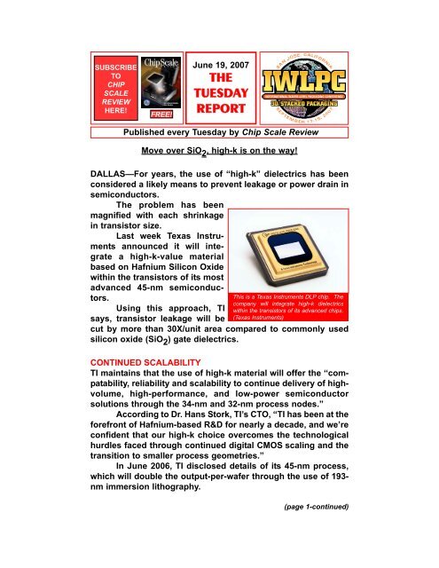
SUBSCRIBETOCHIPSCALEREVIEWHERE!FREE!June 19, 2007THETUESDAYREPORTPublished every Tuesday by <strong>Chip</strong> <strong>Scale</strong> <strong>Review</strong>Move over SiO 2 , high-k is on <strong>the</strong> way!DALLAS—For years, <strong>the</strong> use of “high-k” dielectrics has beenconsidered a likely means to prevent leakage or power drain insemiconductors.The problem has beenmagnified with each shrinkagein transistor size.Last week Texas Instrumentsannounced it will integratea high-k-value materialbased on Hafnium Silicon Oxidewithin <strong>the</strong> transistors of its mostadvanced 45-nm semiconductors.Using this approach, TIsays, transistor leakage will beThis is a Texas Instruments DLP chip. Thecompany will integrate high-k dielectricswithin <strong>the</strong> transistors of its advanced chips.(Texas Instruments)cut by more than 30X/unit area compared to commonly usedsilicon oxide (SiO 2 ) gate dielectrics.CONTINUED SCALABILITYTI maintains that <strong>the</strong> use of high-k material will offer <strong>the</strong> “compatability,reliability and scalability to continue delivery of highvolume,high-performance, and low-power semiconductorsolutions through <strong>the</strong> 34-nm and 32-nm process nodes.”According to Dr. Hans Stork, TI’s CTO, “TI has been at <strong>the</strong>forefront of Hafnium-based R&D for nearly a decade, and we’reconfident that our high-k choice overcomes <strong>the</strong> technologicalhurdles faced through continued digital CMOS scaling and <strong>the</strong>transition to smaller process geometries.”In June 2006, TI disclosed details of its 45-nm process,which will double <strong>the</strong> output-per-wafer through <strong>the</strong> use of 193-nm immersion lithography.(page 1-continued)
Move over SiO 2 , high-k is on <strong>the</strong> way! (continued)Through various techniques, TI says it will also achievea 30 percent increase in performance of its SoC processors,while cutting power consumption by 40 percent.TI expects to sample a 45-nm wireless chip in 2007, withproduction beginning by mid-2008. High-k dielectrics will beadded in later versions of <strong>the</strong> 45-nm process for TI’s highestperformancechips.CVD PROCESSTI will leverage a CVD process to deposit Hafnium SiliconOxide (HfSiO) followed by reaction with a downstream nitrogenplasma to form HfSiON.Although <strong>the</strong> benefits of Hafnium-based dielectrics havebeen widely recognized for <strong>the</strong>ir ability to reduce leakage,implementation earlier presented several hurdles.These included <strong>the</strong> lack of electrical compatibility withstandard CMOS processes, as well as challenges in matching<strong>the</strong> carrier mobility and threshold voltage stability that siliconoxide-basedgate dielectrics delivered.TI says it has been able to solve <strong>the</strong> earlier challenges byimplementing <strong>the</strong> nitrided CVD technique. [ti.com]JCET/JCAP opens North American HQ in FremontFREMONT, Calif.—Jiangsu Changdian Electronics TechnologyCo. (JCET) and its subsidiary, Jiangsu Changdian AdvancedPackaging Co. (JCAP) have established its North Americanheadquarters in Fremont.The new operation is headed by GM Dr. Weiping (Bill) Li.He will be primarily responsible for sales and marketing activitiesin North America.Founded in 1972, JCET/JCAP is <strong>the</strong> leading packagingservice provider in China, according to Dr. Li.“We offer a broad product portfolio ranging from waferbumping, WLCSP to leadframe packaging and testing.JCET/JCAP also has strong IP positions in Cu pillar bumpingand FBP (QFN-type) packaging.”The company has been publicly traded on <strong>the</strong> ShanghaiStock Exchange since 2003. JCET/JCAP is a ISO9001,ISO14001 and TS16949 certified company and became a certified"Sony Green Partner" in early 2007.(page 2-continued)
JCET/JCAP opens North American HQ (continued)In <strong>the</strong> past five years, according to Dr. Li, JCET/JCAPhas experienced about a 30 percent compound annual growthrate with 2006 revenues reaching $240 million.JCET/JCAP has a broad customer base, with about 50percent of its revenue derived from overseas markets.The company has regional offices and customer serviceacross China, Europe, Taiwan and <strong>the</strong> U.S.For fur<strong>the</strong>r information, contact JCET North AmericaOperations, 41341 Joyce Ave., Fremont, CA 94539. Phone. (510)573-3612, email: bli@jcet-us.com. [jcet-us.com]Amkor and UTAC sign cross-licensing agreementCHANDLER, ARIZ.—Amkor Technology Inc., Chandler, andUnited Test and Assembly Center Ltd. (UTAC), Singapore, havesigned a multi-year package cross-licensing agreement.Amkor will license its MicroLeadFrame (MLF) patents toUTAC and UTAC will license its QFN patents to Amkor.The contract covers <strong>the</strong> licensing of intellectual propertyrights and <strong>the</strong> transferof associated packagingtechnologies.The MLF packageis Amkor’s versionof a QFN leadframebased,near-chip-scalepackage.The packagefeatures an exposeddie paddle and leadson <strong>the</strong> bottom.Amkor says it has shipped about five billion MLF packagessince <strong>the</strong>ir introduction in <strong>the</strong> late 1990s. [amkor.com]Do you feel likeyour internationalmarketing plansare riding ona slow boat toChina?Amkor has licensed its MicroLeadFrame patents to UTAC ina cross-licensing agreement with <strong>the</strong> Singapore-basedassembler.(page 3)
XSIL appoints Farrell CEO, Cheng Asia-Pacific regional mgr.DUBLIN, IRELAND—Brian Farrell has replaced Peter Conlon asCEO of XSIL Ltd., a maker of laser micro-machiningsystems.Conlon has assumed <strong>the</strong> company’s chairmanship.Farrell is an XSIL founder and has been vicepresident of engineering since <strong>the</strong> company beganin April 2000.He earned a bachelor’s degree in ma<strong>the</strong>maticsand a degree in mechanical engineering from TrinityCollege, Dublin, as well as a master’s degree inengineering design from University College, Dublin.The company also announced <strong>the</strong> appoin<strong>tm</strong>ent ofFrancis Cheng as Asia-Pacific regional manager,based in Hsin-Chu, Taiwan.He earlier served wtih Spirox Corp. and AiPC inChengTaiwan.Cheng earned a master’s degree in engineering from <strong>the</strong>Institution of Electronics of <strong>the</strong> National Chiao-Tung University,Taiwan. [xsil.com]Naudin joins U.S. Export Authority in new sales postFarrellSAN JOSE— U.S. Export Authority Inc. (USEA) and its affiliatedproduction company, Best Electronics and ComponentsCompany Inc., (BECCI), a provider of contract testingof analog and mixed signal semiconductors,has hired Fabian Naudin as director of worldwidesales. This is a new position.An industry veteran with more than 20 yearsexperience, Naudin <strong>report</strong>s to Fred Kinder, CEO andpresident of both companies.NaudinNaudin was most recently director of western sales forAmkor Technology Inc. He served earlier Foton, ICOS VisionSystems, and Kulicke & Soffa Industries. [usea.com]THE TUESDAY REPORT(TM)is published every Tuesday, except on federal and California state holidays,by <strong>Chip</strong> <strong>Scale</strong> <strong>Review</strong>. Copyright © Gene Selven & Associates Inc., 2007. Allrights reserved. To contact <strong>the</strong> office of publication, phone 408/996-7016.Publisher Gene Selven gselven@aol.comEditor Ron Iscoff chipscale@gmail.comSenior Editor Terrence E. Thompson tethompson@aol.com(page 4)