Experiment 3: Grounding and Shielding
Experiment 3: Grounding and Shielding
Experiment 3: Grounding and Shielding

Create successful ePaper yourself
Turn your PDF publications into a flip-book with our unique Google optimized e-Paper software.
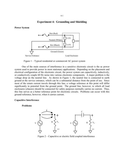
4-1<br />
<strong>Experiment</strong> 4: <strong>Grounding</strong> <strong>and</strong> <strong>Shielding</strong><br />
Power System<br />
Hot (Red)<br />
Neutral (White)<br />
Hot (Black)<br />
115V<br />
115V<br />
230V<br />
Ground (Green)<br />
Service Entrance<br />
Load Enclosure<br />
Figure 1 – Typical residential or commercial AC power system<br />
One of the main sources of interference in a sensitive electronic circuit is the ac power<br />
system used to provide power in most stationary applications. Depending on the placement <strong>and</strong><br />
electrical configuration of the electronic circuit, the power system can capacitively, inductively,<br />
or conductively couple 60 Hz noise into various electronic components. A major problem is the<br />
voltage drop on the neutral line. As shown in Figure 1, the neutral line is connected to earth<br />
ground at the service entrance, which can be a substantial distance from the point of use. Since<br />
most of the return current travels through this line, a voltage reference at this point will differ<br />
significantly in potential from the ground point. The ground line, however, to which all load<br />
enclosures (chassis) should be connected for safety purposes normally carries no current. Thus,<br />
this line serves as a better reference point for electronic circuits. Problems can occur with this<br />
ground reference, however, when it carries current.<br />
Capacitive Interference<br />
Problems<br />
E<br />
C<br />
V<br />
R<br />
V n<br />
V<br />
R<br />
V n<br />
Figure 2 – Capacitive or electric field coupled interference
4-2<br />
Capacitive, or electric field coupled interference occurs when a fringing electric<br />
field is large enough to produce a significant displacement current in an electronic circuit. Under<br />
these conditions the fringing electric field can be modeled as a capacitance with a value<br />
approximately given by<br />
πε<br />
C =<br />
−1 D<br />
(1)<br />
cosh<br />
d<br />
where D is the distance between the noise source <strong>and</strong> the electronic circuit, d is the average wire<br />
diameter, <strong>and</strong> ε is the dielectric permittivity of the environment. Considering the equivalent<br />
circuit shown on the right h<strong>and</strong> side of Figure 2, the noise voltage in the electronic circuit is<br />
given by<br />
R<br />
V n = V<br />
1<br />
(2)<br />
R +<br />
jωC<br />
where V is the voltage of the noise source <strong>and</strong> R is the effective resistance of the electronic<br />
circuit. At low frequencies the rms magnitude of the interference in the electronic circuit is then<br />
|V n | = ωRCV<br />
(3)<br />
So, the magnitude of the interference increases with the frequency of the source <strong>and</strong> the effective<br />
resistance of the electronic circuit.<br />
Remedies<br />
The remedies for capacitive or electric field coupling are relatively straightforward.<br />
From equation (1) it is clear <strong>and</strong> intuitive that the electronic circuit should be as far from the<br />
noise source as possible. Another remedy is to provide electrostatic or conductive shielding<br />
around the electronic circuit connected to a point of fixed potential such as ground. This<br />
terminates the fringing electric fields before they can interact with the relevant circuit. In this<br />
experiment we will use grounded aluminum foil for this purpose.<br />
Inductive Interference<br />
Problems<br />
H<br />
M<br />
I<br />
I<br />
V n<br />
Figure 3 – Inductive or magnetic field coupled interference
4-3<br />
According to Faraday’s law of induction, a voltage will be induced in a circuit<br />
which is linked by the fringing magnetic flux lines of a wire with a time varying electric current.<br />
From an electric circuit point of view, this can be represented by a mutual inductance <strong>and</strong> the<br />
noise voltage is given by<br />
dλ<br />
V n = =<br />
dt<br />
dI<br />
M<br />
dt<br />
(4)<br />
where λ is the flux linkage <strong>and</strong> M is the mutual inductance. If the interference source is<br />
sinusoidal in time, the magnitude of the induced noise voltage is<br />
|V n | = ωMI.<br />
(5)<br />
As with capacitive coupling, in the absence of metallic shielding around the circuit, we expect<br />
inductively coupled interference to increase with the frequency of the noise source.<br />
Remedies<br />
One obvious remedy is to make the circuit as small as possible by using shorter<br />
connections. A smaller circuit is linked by fewer fringing magnetic flux lines. Orientation is<br />
also important. If the portion of the electronic circuit that is picking up the magnetic interference<br />
is parallel to the magnetic flux lines, the linkages will be small <strong>and</strong> less voltage will be induced<br />
in the circuit. Magnetic shielding of the interference source or the electronic circuit is also an<br />
effective remedy at low frequencies. In this experiment we will examine all of these remedies.<br />
At higher frequencies coaxial cable will reduce interference due to skin effect in the<br />
shield. The mutual inductance then has the form<br />
M = M 0<br />
⎛ d ⎞<br />
exp⎜<br />
− ⎟<br />
⎝ δ ⎠<br />
(6)<br />
Where d is the thickness of the shield <strong>and</strong><br />
δ =<br />
2<br />
σµω<br />
(7)<br />
is the skin depth. In equation (7), σ is the conductivity of the shield material <strong>and</strong> µ is its<br />
magnetic permeability. If we calculate skin depth for copper at 60 Hz we obtain<br />
δ = 0.86 cm = 0.34 in.<br />
(8)<br />
which does not reduce the coupling very much at 60 Hz for any normal shield thickness.
4-4<br />
Conductive Interference<br />
Common Power Supply <strong>and</strong> Common Ground<br />
R<br />
R<br />
R S<br />
Ckt<br />
1<br />
I 1 +I 2 I 2<br />
Ckt<br />
V 1<br />
V 2<br />
2<br />
V<br />
Figure 4 – Circuit showing the effects of common power supply<br />
The problems associated with conductive interference are the most difficult to remedy.<br />
Figure 4 indicates a potential problem that will be encountered using a common power supply.<br />
For example, if we look at the voltage across circuit 2, we find that<br />
V 2 = V – (R S + R)(I 1 + I 2 ) – RI 2 .<br />
(9)<br />
That is, the voltage across circuit 2 depends upon the current through circuit 1 because of the<br />
resistance, R, of the connecting wire between the circuits <strong>and</strong> the source resistance, R S . If<br />
Circuit 1 is a typically noisy digital circuit <strong>and</strong> circuit 2 is a sensitive analog circuit, there is a<br />
problem.<br />
Partial Remedy<br />
R<br />
R<br />
C<br />
I 1 I 2<br />
R S Ckt<br />
V 1<br />
Ckt Ckt V 2<br />
1<br />
22<br />
C<br />
V
4-5<br />
Figure 5 – Stellate connection to power supply <strong>and</strong> ground<br />
Figure 5 shows a partial solution to the problem. In this circuit there is a single point or stellate<br />
connection to the power supply <strong>and</strong> a single point connection to ground. In this connection the<br />
interference due to the resistance R of the connecting wire is eliminated but the interference due<br />
to R S remains. The effect of R S could be further reduced by connecting a capacitor, C, across<br />
each circuit to ground, as shown in the figure.<br />
Ground Loop or Common Mode Interference<br />
R 1<br />
V in<br />
R 2<br />
I g<br />
R g<br />
V S<br />
R 1<br />
Figure 6 – Ground loop<br />
Figure 6 indicates the kind of problem that can occur when there is more than one ground<br />
connection in an electronic circuit. More than one ground connection provides a current path or<br />
ground loop through the ground resistance that results in one apparent ground being at a different<br />
potential than another one. In Figure 6, for example, we see that the input voltage to the<br />
amplifier is given by<br />
V in = V S + I S R g .<br />
(10)<br />
To avoid this problem we can eliminate one of the ground connections. As indicated in Figure 7<br />
it is still possible, however, to have a virtual ground loop with only one ground connection. This<br />
V S<br />
C<br />
V in<br />
R 2<br />
I g<br />
R g
4-6<br />
Figure 7 – Virtual ground loop<br />
can be caused by capacitive coupling. Stellate grounding is the preferred mode for electronic<br />
circuits operating at frequencies less than about 1 MHz. Above about 10 MHz the self<br />
inductance of long ground lines becomes a problem <strong>and</strong> multi-point grounding using a ground<br />
plane is usually preferred.<br />
Remedies<br />
The obvious solution to ground loop problems is to use only one ground point reference<br />
in an electronic circuit. As a general rule this is best placed at the most sensitive part of the<br />
circuit: usually at an amplifier input. Avoid the inappropriate use of coaxial cables since they<br />
ground everything to everything else. Differential amplifiers were designed <strong>and</strong> developed to<br />
reduce the effects of common mode signals in electronic circuits. A high common mode<br />
rejection ratio (CMRR) can take care of many of these interference problems. When all else fails<br />
one can always try an optoelectronic isolator or an isolation transformer.<br />
<strong>Experiment</strong>:<br />
Equipment List<br />
1 Printed Circuit Board with AD521 Instrumentation Amplifier<br />
1 Printed Circuit Board Fixture<br />
1 Screw Driver<br />
1 Specially Mounted Inductor, 47 mH, 316 Ω, 200 kHz Self Resonance<br />
1 Cylindrical Magnetic Shield<br />
Procedure<br />
Plug the circuit board into the test fixture. Connect the circuit shown in Figure 8 with an R of<br />
100 Ω. This should result in a gain of 1000 (see table in AD521 data sheet). R should be a ¼<br />
watt resistor mounted using a double banana-to-binding-post adapter <strong>and</strong> other adapters to<br />
minimize circuit area. Run a short jumper from jack 21 to 11. Power up the board <strong>and</strong> confirm<br />
+15VDC<br />
8<br />
20 k Gain Trim<br />
+In<br />
- In<br />
17<br />
21<br />
R<br />
13<br />
14<br />
8<br />
95.3k<br />
1<br />
14<br />
10<br />
13<br />
12<br />
AD521<br />
11 7<br />
2 6<br />
3 4<br />
5<br />
7<br />
Output<br />
-15VDC<br />
10 k Offset<br />
5 Trim 11<br />
Gnd
4-7<br />
Figure 8 – Instrumentation amplifier circuit<br />
that you get a differential gain of 1000 at 1kHz. You may have to adjust the 20k potentiometer<br />
to achieve a gain of 1000. Adjust the 10 kΩ potentiometer (offset null) to set the DC level of the<br />
output to zero; check this null from time to time. Be careful to avoid ground loops in wiring this<br />
setup. Make sure the contacts of the PC board are clean <strong>and</strong> that the banana plugs are securely<br />
connected to their wires.<br />
Input<br />
17<br />
21<br />
R<br />
13<br />
14<br />
8 +15V<br />
Gain 1000<br />
5 -15V<br />
11<br />
7<br />
Output<br />
Input<br />
17<br />
21<br />
R<br />
13<br />
14<br />
8 +15V<br />
Gain<br />
1000<br />
5 -15V<br />
11<br />
7<br />
Output<br />
(a) Differential gain circuit<br />
(b) Common mode gain circuit<br />
Figure 9 - Common Mode Rejection Ratio (CMRR) Measurement<br />
1. Common Mode Rejection Ratio: First measure the differential gain of the circuit of Figure<br />
9(a) at frequencies from 10 Hz to 100 kHz; use a 1, 2, 5 frequency step sequence. The<br />
differential mode input voltage should normally be about 10 mV peak-to-peak.<br />
Next measure the common mode gain of the circuit of Figure 9(b) (run a short jumper<br />
from jack 21 to 17) at frequencies from 10 Hz to 100 kHz; use a 1, 2, 5 frequency step sequence.<br />
The common mode input voltage should be about 5 V peak-to-peak.<br />
8<br />
+15V<br />
1 meter long unshielded cable<br />
17<br />
13<br />
14<br />
Gain<br />
7<br />
Output<br />
10 MegOhms<br />
21<br />
11<br />
5<br />
-15V<br />
Figure 10 - Capacitive Coupling Circuit
4-8<br />
2. Capacitive Coupling: In this part you will study the effects of electric interference by<br />
capacitive coupling into the circuit of Figure 10. Connect the circuit shown in Figure 10. Set the<br />
differential gain to 10 by changing the value of R from 100 Ω to 10 kΩ. Plug a 10 MΩ resistor<br />
into banana jack 21, shorted to 11; <strong>and</strong> connect it by way of a 1 m long unshielded cable to<br />
jack 17; allow the cable to make a broad loop on the bench top. Examine the 60 Hz picked up.<br />
Look at the output in both the time <strong>and</strong> frequency domain. Now take a large sheet of aluminum<br />
foil, ground it to jack 11 at one corner, <strong>and</strong> observe the 60 Hz pickup as you move the foil near<br />
the loop. Finally, wrap the loop <strong>and</strong> observe the 60 Hz pickup with the foil grounded.<br />
8<br />
+15V<br />
Input<br />
Coaxial Cable<br />
16<br />
17<br />
100Ω<br />
21<br />
13<br />
14<br />
Gain 1000<br />
5<br />
11<br />
-15V<br />
7<br />
Output<br />
Figure 11 - Differential Unbalance Circuit<br />
3. Differential Unbalance: Now you will study the effects of differential unbalance (unequal<br />
input impedances). Connect the circuit of Figure 11. Switch back to a gain of 1000 (change R<br />
back to 100 Ω). Run a coax from the signal generator to banana jack 16 taking care that it is<br />
grounded only at the generator (this will require creative plugging on your part!). Connect 16 to<br />
21 via roughly 2 kΩ <strong>and</strong> 16 to 17 via a sequence of fixed resistors, R. Set the generator to 1 V<br />
pk-pk at 1 kHz <strong>and</strong> study |V out | as a function of R as the latter is varied from 10 Ω to 20 kΩ in an<br />
approximate 1, 2, 5 sequence; take additional points as needed to resolve any fine structure you<br />
suspect or discover.
4-9<br />
1 BNC 8<br />
+15V<br />
2 meter long<br />
coaxial cable<br />
1<br />
1 MegΩ<br />
2<br />
18 BNC<br />
17<br />
100 Ω<br />
21<br />
13<br />
14<br />
Gain<br />
Gain 1000<br />
5<br />
-15V<br />
7<br />
Output<br />
18<br />
11<br />
Figure 12 - Magnetic Interference <strong>and</strong> <strong>Shielding</strong> Circuit<br />
4. Magnetic Interference: Finally, you will study magnetic interference <strong>and</strong> shielding. Connect<br />
the circuit of Figure 12. Set the AD521 to a gain of 1000 <strong>and</strong> power it up. Connect the BNC<br />
plugs 18 <strong>and</strong> 1 with 2 m of coax. Then jumper jacks 21 <strong>and</strong> 11. Connect 1 <strong>and</strong> 2 via 1 MΩ<br />
jumper 2 <strong>and</strong> 21; jumper 18 <strong>and</strong> 21; jumper 1 <strong>and</strong> 17. Connect jack 7 to the scope. This gives a<br />
preamplification of 1000 with an input impedance of 1 MΩ. Now set the frequency to 1 kHz,<br />
connect the function generator with a 20 V pk-pk output to the plastic mounted, 47 mH inductor,<br />
<strong>and</strong> observe V out as:<br />
(a) The secondary loop orientation is maintained <strong>and</strong> its area altered with the<br />
inductor both inside <strong>and</strong> outside the secondary loop.<br />
(b) The 47 mH inductor is centered at one point <strong>and</strong> slowly reoriented in the<br />
spherical coordinates Φ <strong>and</strong> Θ (0 < Φ < 2π ; 0 < Θ < π) . Take z along the inductor<br />
axis <strong>and</strong> perpendicular to the bench top.<br />
(c)<br />
outside the loop.<br />
The inductor is moved about in the plane of the loop both inside <strong>and</strong><br />
(d) With the arrangement above, fix a multi-coiled secondary loop in a place<br />
where the pickup is large with the generator at 20 V pk-pk. Measure Vout as a function of<br />
frequency as f is increased in a suitable sequence from 10 Hz to 100 kHz; repeat with the shield<br />
in place over the inductor. (Take note that you may wish to explain the results from different<br />
frequency ranges by invoking different mechanisms. You may therefore wish to deviate from<br />
the st<strong>and</strong>ard 1, 2, 5 frequency sequence while taking data. Advance planning could prove useful<br />
here.)<br />
Write Up<br />
1. Provide on the same graph sheet plots of the differential gain |a d | <strong>and</strong> |CMRR| as<br />
functions of frequency. How do these results compare with the specs in the AD521 data sheet
4-10<br />
2. Describe <strong>and</strong> discuss your results on electrostatic shielding.<br />
3. Plot |V out | / |V gen | as a function of R. Explicitly <strong>and</strong> unambiguously explain the variation<br />
noted.<br />
4. Describe <strong>and</strong> qualitatively explain the area <strong>and</strong> orientation results. Plot the |V out | / |V gen |<br />
vs. f data from part (d) of the experiment <strong>and</strong> qualitatively explain them. Be brief, but be very<br />
sure to set forth unambiguously a clear physical explanation of the observed phenomena; a<br />
simple recapitulation of the salient features of your plot will not suffice.<br />
5. Consider the following problem: You are plagued by pure 60 Hz magnetic interference of<br />
the same magnitude as your desired signal. The power in the desired signal is spread uniformly<br />
over 40-90 Hz, thereby precluding normal filtering; <strong>and</strong> you can neither eliminate the noise<br />
source nor shield the experiment from it. Explain in detail how the circuit in Figure 13 can help.<br />
In particular, quantitatively evaluate the behavior of the circuit between points S <strong>and</strong> S’<br />
60<br />
Hz<br />
115/12.6<br />
CT<br />
10kΩ<br />
Suggested Reading<br />
∞<br />
R = 10kΩ r = 100kΩ C = 1µF<br />
S<br />
R<br />
Figure 13 - 60 Hz interference circuit<br />
r<br />
C<br />
R<br />
∞<br />
S’<br />
Noisy<br />
Signal<br />
Input<br />
x 1<br />
Output<br />
R. A. Bartkowiak, Electric Circuits, (Intext, New York, 1973).<br />
J. D. Kraus, Electromagnetics, (McGraw-Hill, New York, 1953).<br />
R. Morrison, <strong>Grounding</strong> <strong>and</strong> <strong>Shielding</strong> Techniques in Instrumentation, (Wiley, New York,<br />
1971).<br />
H. W. Ott, Noise Reduction Techniques in Electronic Systems, (Wiley, New York,1976).
4-11