

AN-561 - Analog Devices
AN-561 - Analog Devices
AN-561 - Analog Devices

You also want an ePaper? Increase the reach of your titles
YUMPU automatically turns print PDFs into web optimized ePapers that Google loves.
a<br />
<strong>AN</strong>-<strong>561</strong><br />
APPLICATION NOTE<br />
One Technology Way • P.O. Box 9106 • Norwood, MA 02062-9106 • 781/329-4700 • World Wide Web Site: http://www.analog.com<br />
REV. 0<br />
AD7416 Connects to the PIC16F84 via Emulated I 2 C ® Interface<br />
INTRODUCTION<br />
This application note describes the requirements to control<br />
the AD7416 via a PIC microcontroller by emulating<br />
an I 2 C bus interface. It will provide code examples and<br />
descriptions of both hardware and software. Although<br />
this application uses the PIC16F84, it is possible to<br />
modify the code to use other microcontrollers from<br />
Microchip and other suppliers. Additional information<br />
about the AD7416 is available from <strong>Analog</strong> <strong>Devices</strong><br />
(www.analog.com) and information about the PIC microcontroller<br />
is available from Microchip (www.microchip.com).<br />
Both should be consulted in conjunction with this application<br />
note.<br />
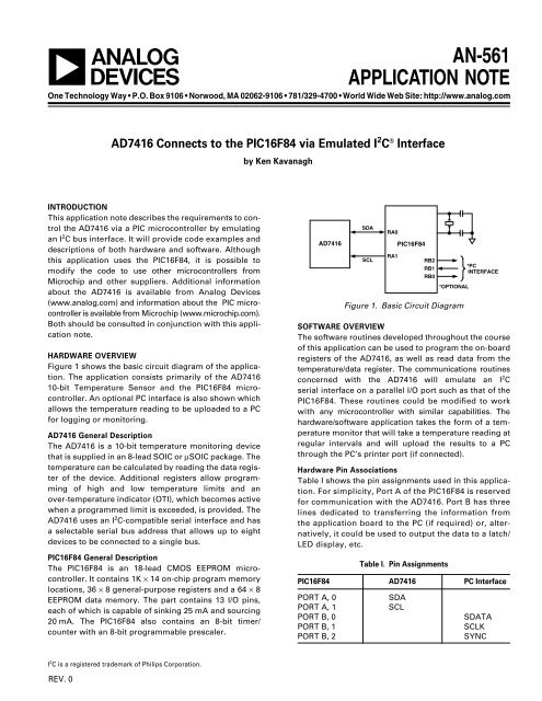
HARDWARE OVERVIEW<br />
Figure 1 shows the basic circuit diagram of the application.<br />
The application consists primarily of the AD7416<br />
10-bit Temperature Sensor and the PIC16F84 microcontroller.<br />
An optional PC interface is also shown which<br />
allows the temperature reading to be uploaded to a PC<br />
for logging or monitoring.<br />
AD7416 General Description<br />
The AD7416 is a 10-bit temperature monitoring device<br />
that is supplied in an 8-lead SOIC or µSOIC package. The<br />
temperature can be calculated by reading the data register<br />
of the device. Additional registers allow programming<br />
of high and low temperature limits and an<br />
over-temperature indicator (OTI), which becomes active<br />
when a programmed limit is exceeded, is provided. The<br />
AD7416 uses an I 2 C-compatible serial interface and has<br />
a selectable serial bus address that allows up to eight<br />
devices to be connected to a single bus.<br />
PIC16F84 General Description<br />
The PIC16F84 is an 18-lead CMOS EEPROM microcontroller.<br />
It contains 1K × 14 on-chip program memory<br />
locations, 36 × 8 general-purpose registers and a 64 × 8<br />
EEPROM data memory. The part contains 13 I/O pins,<br />
each of which is capable of sinking 25 mA and sourcing<br />
20 mA. The PIC16F84 also contains an 8-bit timer/<br />
counter with an 8-bit programmable prescaler.<br />
I 2 C is a registered trademark of Philips Corporation.<br />
by Ken Kavanagh<br />
SDA<br />
AD7416 PIC16F84<br />
SCL<br />
RA0<br />
RA1<br />
RB2<br />
RB1<br />
*PC<br />
INTERFACE<br />
RB0<br />
*OPTIONAL<br />
Figure 1. Basic Circuit Diagram<br />
SOFTWARE OVERVIEW<br />
The software routines developed throughout the course<br />
of this application can be used to program the on-board<br />
registers of the AD7416, as well as read data from the<br />
temperature/data register. The communications routines<br />
concerned with the AD7416 will emulate an I 2 C<br />
serial interface on a parallel I/O port such as that of the<br />
PIC16F84. These routines could be modified to work<br />
with any microcontroller with similar capabilities. The<br />
hardware/software application takes the form of a temperature<br />
monitor that will take a temperature reading at<br />
regular intervals and will upload the results to a PC<br />
through the PC’s printer port (if connected).<br />
Hardware Pin Associations<br />
Table I shows the pin assignments used in this application.<br />
For simplicity, Port A of the PIC16F84 is reserved<br />
for communication with the AD7416. Port B has three<br />
lines dedicated to transferring the information from<br />
the application board to the PC (if required) or, alternatively,<br />
it could be used to output the data to a latch/<br />
LED display, etc.<br />
Table I. Pin Assignments<br />
PIC16F84 AD7416 PC Interface<br />
PORT A, 0 SDA<br />
PORT A, 1 SCL<br />
PORT B, 0 SDATA<br />
PORT B, 1 SCLK<br />
PORT B, 2 SYNC
<strong>AN</strong>-<strong>561</strong><br />
SOFTWARE DESCRIPTION<br />
This section will deal with the specific routines developed<br />
for the PIC16F84 to communicate with the AD7416<br />
by emulating the I 2 C serial bus. The routines discussed<br />
here are not intended as a definitive programming structure<br />
but, rather, as a guide to users who wish to develop<br />
their own routines. This section will discuss the initialization<br />
of the PIC processor, the configuration of the<br />
ports, and the subroutines required to communicate<br />
with the AD7416. As with many programming languages,<br />
labels will be used to identify particular registers<br />
used in the PIC16F84. The use of labels makes<br />
programs easier to read and, if necessary, debug. Labels<br />
are represented in bold italic format (e.g., LABELS). A list of<br />
all labels used in the program is given in Appendix A.<br />
PIC16F84 Initialization Routine<br />
When power is first applied to the PIC16F84 a number<br />
of initialization routines need to be done. These are<br />
required to set the configuration (input or output) and<br />
state (high or low) of the I/O ports, as well as setting up<br />
the timer to generate interrupts at regular intervals,<br />
allowing the temperature to be read periodically. The<br />
listing for the initialization routine is given below.<br />
Listing 1. Port Initialization<br />
PORTINIT<br />
MOVLW 0xFF<br />
MOVWF PORTA ;set port lines high<br />
MOVLW 0x4 ;set sclk,sdata low<br />
MOVWF PORTB ;& sync high (PC interface)<br />
BSF STATUS,RP0 ;point to the OPTION<br />
;and TRIS registers<br />
MOVLW 0x00<br />
MOVWF TRISA ;make portA output<br />
MOVLW 2 ;setup portB<br />
MOVWF TRISB ;sclk=i/p,<br />
;sync & sdata=o/p<br />
MOVLW b’10000111' ;set the timer<br />
;prescaler to 256<br />
MOVWF OPTREG ;and copy to OPTREG<br />
BCF STATUS,RP0 ;point to port registers<br />
RETURN ;exit subroutine<br />
Start and Stop Frame Routines<br />
In the I 2 C protocol, all transfers of information must begin<br />
with a Start Frame and end with a Stop Frame. In the idle<br />
state both SDA and SCL lines will be high. A Start Frame<br />
is generated by bringing SDA low while SCL is high.<br />
This is shown in Figure 2. Similarly a Stop Frame is generated<br />
by bringing the SDA line high while SCL is high.<br />
This is shown in Figure 3.<br />
–2–<br />
SCL<br />
SDA<br />
SCL<br />
SDA<br />
PORT = 0x3<br />
PORT = 0x2<br />
PORT = 0x0<br />
I 2 C PROTOCOL PIC16F84<br />
EQUIVALENT<br />
Figure 2. Start Frame<br />
STARTFR<br />
Listing 2. Generating Start Frame Signal<br />
;generates a start signal<br />
;assumes both lines are<br />
;outputs and both are high<br />
MOVLW 0x2 ;Bring SDA Low<br />
MOVWF PORTA<br />
MOVLW 0x0 ;SDA and SCL both low<br />
MOVWF PORTA ;Start Frame Generated<br />
RETURN ;exit subroutine<br />
SCL<br />
SDA<br />
SCL<br />
SDA<br />
PORT = 0x0<br />
PORT = 0x2<br />
PORT = 0x3<br />
I 2 C PROTOCOL PIC16F84<br />
EQUIVALENT<br />
Figure 3. Stop Frame<br />
Listing 3. Generating a Stop Frame Signal<br />
STOPFR ;generate a stop frame<br />
;assmumes both lines are output<br />
;and both are low<br />
MOVLW 2 ;bring SCL high<br />
MOVWF PORTA<br />
MOVLW 3 ;SCL and SDA both high<br />
MOVWF PORTA ;Stop Frame generated<br />
RETURN ;exit subroutine<br />
With routines for generating Start and Stop Frames generated,<br />
it is now necessary to develop routines that will<br />
allow the user to write to the registers of the AD7416.<br />
Figure 7 in the AD7416 data sheet shows a timing diagram<br />
for such an operation. After a Start Frame signal<br />
has been issued the microcontroller must transmit<br />
seven bits containing the address of the device it wishes<br />
to communicate with. The eighth bit tells the AD7416<br />
that the next operation will be a write or a read operation,<br />
and the ninth bit allows the AD7416 to issue an<br />
acknowledgment. For simplicity, the seven address bits<br />
and the R/W bit will be combined into one byte and the<br />
status of the ACK pulse will be read but not acted upon.<br />
Figure 4 shows a flowchart of the write operation and<br />
Listing 4 shows the code.<br />
REV. 0
REV. 0<br />
BYTE TO BE TR<strong>AN</strong>SMITTED<br />
LOCATED IN TXVAL REGISTER<br />
LOAD COUNT WITH<br />
NUMBER OF BITS<br />
TO SEND (=8)<br />
ROTATE TXVAL SO THAT<br />
MSB MOVES INTO<br />
CARRY BIT<br />
NO<br />
BRING SDA <strong>AN</strong>D<br />
SCL LOW<br />
BRING SCL HIGH<br />
BRING SCL LOW<br />
IS THE<br />
CARRY<br />
BIT SET?<br />
DECREASE COUNT<br />
HAS<br />
COUNT<br />
REACHED<br />
ZERO?<br />
YES<br />
YES<br />
BRING SCL LOW<br />
<strong>AN</strong>D SDA HIGH<br />
BRING BOTH HIGH<br />
BRING SCL LOW<br />
NO<br />
CH<strong>AN</strong>GE SDA LINE TO INPUT<br />
BRING SCL HIGH TEST SDA BIT<br />
BRING SCL LOW<br />
CH<strong>AN</strong>GE SDA LINE TO OUTPUT<br />
EXIT SUBROUTINE<br />
Figure 4. SENDBYTE Flowchart<br />
Listing 4. The SENDBYTE Routine<br />
SENDBYTE ;subroutine to send 8 bits to<br />
;AD7416<br />
MOVLW 8 ;holds the number of bits to<br />
;transmit<br />
MOVWF COUNT ;store in memory location<br />
LOOP<br />
RLF TXVAL ;rotate the msb into carry bit<br />
BC BITHIGH;branch if bit is high?<br />
BITLOW ;send logic 0<br />
MOVLW 0 ;scl, sda low<br />
MOVWF PORTA<br />
MOVLW 2 ;scl high, sda low<br />
MOVWF PORTA<br />
NOP ;let bit settle<br />
MOVLW 0 ;scl,sda low<br />
MOVWF PORTA<br />
GOTO BITDONE;this bit has been<br />
;transmitted<br />
–3–<br />
BITHIGH ;send logic 1<br />
MOVLW 0 ;scl, sda low<br />
MOVWF PORTA<br />
MOVLW 1 ;sda high, scl low<br />
MOVWF PORTA<br />
MOVLW 3 ;scl, sda high<br />
MOVWF PORTA<br />
NOP ;let bit settle<br />
MOVLW 1 ;scl low, sda high<br />
MOVWF PORTA<br />
MOVLW 0<br />
MOVWF PORTA ;both low<br />
BITDONE<br />
DECFSZ COUNT,1;decrease count by 1 and<br />
;repeat if not zero<br />
GOTO LOOP<br />
<strong>AN</strong>-<strong>561</strong><br />
CHECKACK ;look for ACK pulse<br />
;Change sda line to input for ACK<br />
BSF STATUS,RP0;point to TRIS registers<br />
MOVLW 1<br />
MOVWF TRISA ;make sda line an input<br />
BCF STATUS,RP0;point to PORT register<br />
MOVLW 2 ;scl high<br />
MOVWF PORTA<br />
NOP ;let bit settle<br />
MOVF PORTA,W;read the port<br />
BTFSS PORTA,0;check status of ACK bit and<br />
;store in ACKSTATUS register<br />
GOTO ACK0<br />
BSF ACKSTATUS,0;positive ACK received<br />
GOTO NEXT<br />
ACK0<br />
BCF ACKSTATUS,0;negative ACK received<br />
NEXT<br />
MOVLW 0 ;scl low<br />
MOVWF PORTA<br />
;Change port back to output<br />
MOVLW 0 ;preload output register with 0’s<br />
MOVWF PORTA<br />
BSF STATUS,RP0<br />
MOVLW 0<br />
MOVWF TRISA ;make all port line outputs<br />
BCF STATUS,RP0<br />
RETURN ;exit subroutine<br />
The subroutine listed above needs to be called twice in<br />
order to set up the AD7416 for reading the temperature.<br />
The first instance tells a particular device that it is being<br />
addressed and the second instance is used to send the<br />
Address Register Pointer Byte. In the case of the AD7416<br />
this means sending 0hex to the device to select the temperature.<br />
Of course, different registers can be selected<br />
by sending different address values. The user should<br />
consult the AD7416 data sheet for more information.
<strong>AN</strong>-<strong>561</strong><br />
Reading Temperature Data<br />
After the above routines have been called, the AD7416 is<br />
set up to supply temperature data. The temperature data<br />
can be read from the AD7416 in either a 1- or 2-byte read<br />
operation, the latter being the more accurate. For this<br />
application, the 2-byte read operation is used. The two<br />
bytes are stored in the HIGHBYTE and LOWBYTE registers<br />
upon completion and the user can then latch them<br />
to an external device, analyze them further, etc. The<br />
READBYTE function is similar to the SENDBYTE function,<br />
but this time the state of the SDA pin is checked<br />
and the LOWBYTE register is modified accordingly. The<br />
2-byte read operation requires the master device (i.e.,<br />
the PIC16F84) to output a different ACK on each read. In<br />
order to allow the same read routine to provide both<br />
types of ACK pulse, it looks at Bit 1 of the ACKSTATUS<br />
register. The state of this bit will determine what type of<br />
ACK pulse is needed. The listing and basic flowchart are<br />
shown below.<br />
CH<strong>AN</strong>GE SDA LINE<br />
TO INPUT<br />
ROTATE LOWBYTE LEFT<br />
1 BIT <strong>AN</strong>D BRING<br />
SCL HIGH<br />
NO<br />
BRING SCL LOW<br />
LOAD COUNT WITH<br />
NUMBER OF BITS<br />
TO SEND (=8)<br />
IS SDA<br />
HIGH?<br />
DECREASE COUNT<br />
HAS<br />
COUNT<br />
REACHED<br />
ZERO?<br />
YES<br />
YES<br />
CH<strong>AN</strong>GE SDA TO OUTPUT<br />
GENERATE ACK PULSE<br />
EXIT SUBROUTINE<br />
BRING SCL LOW<br />
LSB OF LOWBYTE<br />
SET TO 1<br />
NO<br />
Figure 5. READBYTE Flowchart<br />
–4–<br />
Listing 5. READBYTE Routine<br />
READBYTE ;reads 8 bits from port<br />
;result is stored in LOWBYTE<br />
;change the sda line to input<br />
BSF STATUS,RP0<br />
MOVLW 1<br />
MOVWF TRISA ;make sda line an input<br />
BCF STATUS,RP0<br />
MOVLW 8<br />
MOVWF COUNT<br />
BITLOOP<br />
MOVLW 2 ;SCL high<br />
MOVWF PORTA ;<br />
NOP<br />
NOP; ;small delay<br />
RLF LOWBYTE;rotate - 0 moves into LSB<br />
BTFSS PORTA,0; test the SDA line<br />
GOTO LOGIC0 ; bit is 0<br />
LOGIC1<br />
BSF LOWBYTE,0 ;set the LSB to 1<br />
GOTO NEXTBIT<br />
LOGIC0<br />
BCF LOWBYTE,0; clear the LSB to 0<br />
NOP ;small delay<br />
NEXTBIT<br />
MOVLW 0<br />
MOVWF PORTA ; scl low<br />
DECFSZ COUNT,1; decrease the count<br />
GOTO BITLOOP; repeat if not zero<br />
;now generate master ACK<br />
;Change port back to output<br />
MOVLW 0;preload output register<br />
MOVWF PORTA<br />
BSF STATUS,RP0<br />
MOVLW 0<br />
MOVWF TRISA ;make all port line outputs<br />
BCF STATUS,RP0<br />
BTFSS ACKSTATUS,1 ;what type of ACK req’d?<br />
GOTO MASTERACKLOW ;ACK required<br />
;master NACK<br />
MOVLW 1 ;sda high<br />
MOVWF PORTA<br />
MOVLW 3 ;sda,scl high<br />
MOVWF PORTA<br />
MOVLW 1<br />
MOVWF PORTA ;sda high, scl low<br />
MOVLW 0<br />
MOVWF PORTA ;both low<br />
GOTO ENDOFACK<br />
MASTERACKLOW<br />
MOVLW 2 ;scl high<br />
MOVWF PORTA<br />
MOVLW 0 ;scl low<br />
MOVWF PORTA<br />
ENDOFACK ;leave the port as an output<br />
RETURN<br />
REV. 0
When the program returns from this function the result<br />
is stored in the LOWBYTE register. Since the temperature<br />
data is transmitted MSB first the result needs to be<br />
moved into the HIGHBYTE register before the routine is<br />
called a second time to get the last eight bits of temperature<br />
data. The compete read operation is shown below.<br />
REV. 0<br />
Listing 6. The READTEMPERATURE Routine<br />
READTEMPERATURE<br />
CALL STARTFR ;send start signal<br />
;send address byte<br />
MOVLW 0x91 ;ADDRESS byte - read op<br />
MOVWF TXVAL<br />
CALL SENDBYTE ;transmit the byte<br />
BCF ACKSTATUS,1 ;ACK Req’d for first byte<br />
CALL READBYTE<br />
;move the data into the high result register<br />
MOVF LOWBYTE,0<br />
MOVWF HIGHBYTE<br />
;store the type of ack req’d from master<br />
BSF ACKSTATUS,1 ;NACK Req’d for 2nd byte<br />
CALL READBYTE<br />
CALL STOPFR<br />
The routines described above are all that is required to<br />
configure the PIC16F84 and read temperature data from<br />
the AD7416. Additional routines can be developed that<br />
use the Timer/Counter of the PIC to read temperature<br />
data periodically. Such routines will not be discussed<br />
here but information on how this can be achieved is<br />
available on the PIC16F84 data sheet and in examples on<br />
the Microchip web site. A complete listing of a sample<br />
program, which includes the code sections described<br />
above, is also available from <strong>Analog</strong> <strong>Devices</strong>.<br />
Uploading Data to the PC via the Printer Port<br />
The printer port of a PC provides an easy way to transfer<br />
the temperature data from the PIC to the PC where it<br />
may be logged or monitored. A discussion on the functionality<br />
of the printer port is beyond the scope of this<br />
SYNC<br />
SCLK<br />
SDATA<br />
–5–<br />
<strong>AN</strong>-<strong>561</strong><br />
application note, so only essential details will be mentioned.<br />
What follows is a brief example of how the<br />
temperature data can be sent to a PC using a minimum<br />
wire count, thus preserving I/O lines for other uses. The<br />
temperature data will be sent to the PC one bit at a time<br />
(if a PC is connected to the PIC) starting with the MSB.<br />
The interface uses only three wires (designated SYNC,<br />
SDATA, and SCLK). Figure 6 shows the timing diagram<br />
of the Transmit routine. When the PIC16F84 has read a<br />
temperature result from the AD7416, it will bring the<br />
SYNC line low. It starts decreasing a counter and if it<br />
does not detect a rising clock edge before the counter<br />
reaches zero, it will bring SYNC back high and abort the<br />
transmission of data. This allows the PIC16F84 to continue<br />
reading temperature data if PC is not connected or<br />
the PC software is not running.<br />
When the PIC16F84 detects a rising SCLK edge it sets<br />
RB0 to the same logic level as the MSB of the temperature<br />
data result. The routine continues to monitor SCLK<br />
and when it goes low the bit count is decreased and the<br />
program will wait for another rising edge to transmit the<br />
next bit of data, unless all bits have been transmitted.<br />
After all bits have been transmitted, the program brings<br />
SYNC high to indicate the end of the transfer. Figure 6<br />
shows the timing diagram for the data transfer. Table II<br />
shows the connections between the PIC16F84 and the<br />
appropriate printer port pins.<br />
Table II.<br />
PIC16F84 Printer Port<br />
Name Pin Name Pin 1 Function<br />
RB0 6 SLCT 13 SDATA<br />
RB1 7 INIT 16 2<br />
SCLK<br />
RB2 8 ACK 10 SYNC<br />
NOTES<br />
1 Printer Port Pin Numbers Refer to a 25-pin D-type connector.<br />
2 INIT is Pin 31 on a 36-pin Centronic connector.<br />
D15 D14 D13 D12 D11 D10 D09 D08 D07 D06 D05 D04 D03 D02 D01 D00<br />
Figure 6. PIC16F84 to PC Printer Port Timing Diagram
<strong>AN</strong>-<strong>561</strong><br />
Listing 7. Serial Transmission Routine<br />
SERIALTX<br />
;this routine transmits the HIGHBYTE<br />
;and then the LOWBYTE<br />
MOVLW 8 ;number of bits in HIGHBYTE<br />
MOVWF COUNT<br />
MOVLW 0xFF ;length of TIMEOUT wait<br />
MOVWF TEMP<br />
MOVLW 0<br />
MOVWF PORTB ;sync, sdata low<br />
CLKLOOP ;wait for rising clock edge<br />
DECFSZ TEMP,1 ;reduce timeout count<br />
GOTO NOTIMEOUT; no need for timeout yet<br />
GOTO DONE ; timeout reached- exit routine<br />
NOTIMEOUT<br />
BTFSS PORTB,1<br />
GOTO CLKLOOP;no edge yet<br />
RLF HIGHBYTE ;move msb into carry bit<br />
BC HILOOP ;branch if bit is 1<br />
MOVLW 0 ;put out 0 on sdata<br />
MOVWF PORTB<br />
LOWLOOP<br />
BTFSC PORTB,1;wait until sclk goes low<br />
GOTO LOWLOOP;sclk still high<br />
GOTO DECLOOP;sclk has gone high<br />
HILOOP<br />
MOVLW 1 ;put out 1 on sdata<br />
MOVWF PORTB<br />
LOLOOP<br />
BTFSC PORTB,1;wait until sclk goes low<br />
GOTO LOLOOP ;repeat as necessary<br />
DECLOOP<br />
DECFSZ COUNT,1;decrease bit count<br />
GOTO BITRXD ;repeat as necessary<br />
GOTO STARTLOWBYTE<br />
BITRXD<br />
INCF TEMP ;bit sent so stop<br />
GOTO CLKLOOP;timeout from decrementing<br />
–6–<br />
;HIGHBYTE has been transmitted<br />
MOVLW 8 ;reset the count to<br />
MOVWF COUNT ;transmit LOWBYTE<br />
SCLKTST ;wait for rising clock edge<br />
BTFSS PORTB,1<br />
GOTO SCLKTST;no edge yet<br />
RLF LOWBYTE;move msb into carry bit<br />
BC HILOOP2;branch if bit is 1<br />
MOVLW 0<br />
MOVWF PORTB ;put out 0 on sdata<br />
LOWLOOP2<br />
BTFSC PORTB,1;wait until sclk goes low<br />
GOTO LOWLOOP2 ;sclk still high<br />
GOTO DECLOOP2<br />
HILOOP2<br />
MOVLW 1 ;put out 1 on sdata<br />
MOVWF PORTB<br />
LOLOOP2<br />
BTFSC PORTB,1;wait until sclk goes low<br />
GOTO LOLOOP2 ;repeat as necessary<br />
DECLOOP2<br />
DECFSZ COUNT,1;decrease bit count and<br />
GOTO SCLKTST;repeat if necessary<br />
DONE MOVLW 4 ;bring sync high<br />
MOVWF PORTB<br />
RETURN ;exit subroutine<br />
REV. 0
The corresponding program for the PC is written in Ccode<br />
and can easily be adapted for other languages. The<br />
PC program monitors the SYNC line (ACK in the Status<br />
Register of the printer port), waiting for it to go low.<br />
When it does, the program brings the SCLK pin high<br />
(INIT in the Control Register). Since the PC operates considerably<br />
faster than the microcontroller, a delay is used<br />
to allow the microcontroller to put out a data bit before<br />
the PC reads it. The length of delay required will depend<br />
REV. 0<br />
#include<br />
#include<br />
void main()<br />
{<br />
Listing 8. C-Code Program to Allow a PC to Read Temperature from AD7416/PIC16F84<br />
–7–<br />
<strong>AN</strong>-<strong>561</strong><br />
on both the speed of the PC and that of the microcontroller.<br />
When the delay has expired, the state of the SDATA<br />
bit is tested (SLCT in the Status Register). If the bit is 1,<br />
then a Logic 1 is OR’ed to the Result. If the bit is 0, nothing<br />
is done. As the sequence repeats for the next bit, the<br />
result is left-shifted by one bit so that when all bits have<br />
been tested, Result will contain the 16-bit temperature<br />
data value from the AD7416. The 10 MSBs store the temperature<br />
reading in twos complement format.<br />
int StatusPort=0x379;<br />
int ControlPort=0x37a;<br />
int BitCount;<br />
int ControlReg;<br />
int value;<br />
unsigned int Result;<br />
unsigned int Delay;<br />
ControlReg=inportb(ControlPort);<br />
ControlReg=ControlReg & 0xfb; //bring INIT low<br />
outportb(ControlPort,ControlReg);<br />
while((inportb(StatusPort) & 0x40)!=0);//loop until SYNC goes low<br />
Result=0;<br />
for (BitCount=0;BitCount
<strong>AN</strong>-<strong>561</strong><br />
ACK<br />
SLCT<br />
1 13<br />
14 25<br />
INIT GND<br />
Figure 7. 25-Way Male D-Type Connector<br />
18<br />
36<br />
A0<br />
A1<br />
A2<br />
SLCT<br />
ACK<br />
INIT GND<br />
Figure 8. 36-Way Centronics Connector<br />
V DD<br />
AD7416 PIC16F84<br />
GND<br />
SDA<br />
SCL<br />
10k�<br />
0.1�F<br />
MCLR<br />
RA0<br />
RA1<br />
V DD<br />
5V<br />
OSC1<br />
OSC2<br />
1<br />
19<br />
RB2<br />
GND<br />
RB1<br />
RB0<br />
*PC<br />
INTERFACE<br />
*OPTIONAL<br />
Figure 9. Application Circuit Diagram<br />
–8–<br />
APPENDIX A – PIC16F84 EQUATES<br />
TMR0 EQU 1<br />
PCL EQU 2<br />
STATUS EQU 3<br />
FSR EQU 4<br />
PORTA EQU 5<br />
PORTB EQU 6<br />
EEDATA EQU 8<br />
EEADR EQU 9<br />
PCLATH EQU 0x0A<br />
INTCON EQU 0x0B<br />
TRISA EQU 5<br />
TRISB EQU 6<br />
RP0 EQU 5<br />
RP1 EQU 6<br />
COUNT EQU 0x0C<br />
TEMP EQU 0x0F<br />
TXVAL EQU 0x11<br />
RW EQU 0x12<br />
ACK EQU 0x13<br />
HIGHBYTE EQU 0x14<br />
LOWBYTE EQU 0x15<br />
ACKSTATUS EQU 0x16<br />
TIME1 EQU 0x17<br />
INTCON EQU 0x0B<br />
GIE EQU 0x7<br />
T0IE EQU 0x5<br />
T0IF EQU 0x2<br />
OPTREG EQU 0x81<br />
REV. 0<br />
PRINTED IN U.S.A. E3781–2–4/00 (rev. 0)


