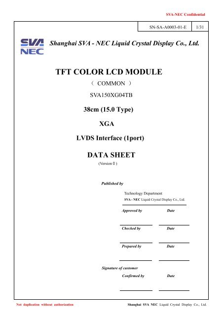
Shanghai SVA - NEC Liquid Crystal Display Co., Ltd ... - Fortec AG
Shanghai SVA - NEC Liquid Crystal Display Co., Ltd ... - Fortec AG
Shanghai SVA - NEC Liquid Crystal Display Co., Ltd ... - Fortec AG

You also want an ePaper? Increase the reach of your titles
YUMPU automatically turns print PDFs into web optimized ePapers that Google loves.
<strong>SVA</strong>-<strong>NEC</strong> <strong>Co</strong>nfidential<br />
SN-SA-A0003-01-E 1/31<br />
<strong>Shanghai</strong> <strong>SVA</strong> - <strong>NEC</strong> <strong>Liquid</strong> <strong>Crystal</strong> <strong>Display</strong> <strong>Co</strong>., <strong>Ltd</strong>.<br />
TFT COLOR LCD MODULE<br />
COMMON <br />
<strong>SVA</strong>150XG04TB<br />
38cm (15.0 Type)<br />
XGA<br />
LVDS Interface (1port)<br />
DATA SHEET<br />
(Version )<br />
Published by<br />
Technology Department<br />
<strong>SVA</strong> - <strong>NEC</strong> <strong>Liquid</strong> <strong>Crystal</strong> <strong>Display</strong> <strong>Co</strong>., <strong>Ltd</strong>.<br />
L<br />
Approved by<br />
Date<br />
Checked by<br />
Date<br />
Prepared by<br />
Date<br />
Signature of customer<br />
<strong>Co</strong>nfirmed by<br />
Date<br />
Not duplication without authorization<br />
<strong>Shanghai</strong> <strong>SVA</strong> <strong>NEC</strong> <strong>Liquid</strong> <strong>Crystal</strong> <strong>Display</strong> <strong>Co</strong>., <strong>Ltd</strong>.
SN-SA-A0003-01-E 2/31<br />
INTRODUCTION<br />
• WARRANTY<br />
<strong>Shanghai</strong> <strong>SVA</strong> <strong>NEC</strong> <strong>Liquid</strong> <strong>Crystal</strong> <strong>Display</strong> <strong>Co</strong>., <strong>Ltd</strong>. (hereinafter called "<strong>SVA</strong>-<strong>NEC</strong>") warrants that this product<br />
meets the product specifications set forth in this document. If this product under normal operation is found to be<br />
non-conforming to the product specifications, and such non-conformance is promptly notified to <strong>SVA</strong>-<strong>NEC</strong> within<br />
one (1) year after the delivery date, and further such non-conformance is solely attributable to <strong>SVA</strong>-<strong>NEC</strong>, <strong>SVA</strong>-<strong>NEC</strong><br />
shall repair the non-conforming product or replace it with a conforming one, free of charge. However, this warranty<br />
does not apply to any non-conformance that can be found easily by incoming inspections or those resulting from any<br />
one of the following<br />
1) Unauthorized or improper repair, maintenance or modification<br />
2) Operation or use against specifications, instructions or warnings given by <strong>SVA</strong>-<strong>NEC</strong><br />
3) Any other causes attributable to customer<br />
In case <strong>SVA</strong>-<strong>NEC</strong> repairs or replaces a product after the one (l)-year warranty period, <strong>SVA</strong>-<strong>NEC</strong> shall be entitled to<br />
charge for such repair or replacement. Those replaced parts shall be covered with six (6)-month warranty period from<br />
the replacement day. Non-conforming products may be replaced with substitutes instead of repair when the manufacture<br />
of this product has been terminated.<br />
EXCEPT AS EXPRESSLY SET FORTH HEREIN, <strong>SVA</strong>-<strong>NEC</strong> DISCLAIMS ANY WARRANTIES,<br />
EXPRESS OR IMPLIED, INCLUDING BUT NOT LIMITED TO MERCHANTABILITY AND FITNESS FOR<br />
A PARTICULAR PURPOSE, AND DISCLAIMS ANY REMEDIES.<br />
• MAINTENANCE<br />
The specifications of maintenance parts may be partially changed within equivalent quality or better. In this<br />
product, <strong>SVA</strong>-<strong>NEC</strong> will not accept to maintain for only mounting parts on circuit board (e.g. connector, fuse, capacitor,<br />
resistor, etc.) and only backlight conformation parts (e.g. reflector sheet, light guide plate, etc.).<br />
If <strong>SVA</strong>-<strong>NEC</strong> is planning discontinuation for this product, <strong>SVA</strong>-<strong>NEC</strong> shall inform it to customers in six (6)-months<br />
advance from the issued date of official agreements. In addition, after product discontinuation, <strong>SVA</strong>-<strong>NEC</strong> may replace<br />
substitutes instead of maintenance parts with whole product.<br />
• CHANGE CONTROL<br />
For the purpose of product improvement, this product design may be changed for specifications, appearance, parts,<br />
circuits and so on. In case a design change is affected on the product specifications, <strong>SVA</strong>-<strong>NEC</strong> shall inform it to<br />
customers in advance.<br />
• HANDLING OF DOUBTFUL POINTS<br />
Any question arising out of, or in connection with, this SPECIFICATION or any matter not stipulated herein will be<br />
settled each time upon consultation between both parties.<br />
Not duplication without authorization<br />
<strong>Shanghai</strong> <strong>SVA</strong> <strong>NEC</strong> <strong>Liquid</strong> <strong>Crystal</strong> <strong>Display</strong> <strong>Co</strong>., <strong>Ltd</strong>.
SN-SA-A0003-01-E 3/31<br />
CONTENTS<br />
INTRODUCTION ....................................................................................................................................................... 2<br />
CONTENTS................................................................................................................................................................. 3<br />
1. OUTLINE ................................................................................................................................................................ 4<br />
1.1 STRUCTURE AND PRINCIPLE.................................................................................................................. 4<br />
1.2 APPLICATIONS............................................................................................................................................ 4<br />
1.3 FEATURES.................................................................................................................................................... 4<br />
2. GENERAL SPECIFICATIONS............................................................................................................................... 5<br />
3. BLOCK DI<strong>AG</strong>RAM ................................................................................................................................................ 6<br />
4. DETAILED SPECIFICATION ................................................................................................................................ 7<br />
4.1 MECHANICAL SPECIFICATIONS ............................................................................................................. 7<br />
4.2 ABSOLUTE MAXIMUM RATINGS............................................................................................................ 7<br />
4.3 ELECTRICAL CHARACTERISTICS .......................................................................................................... 8<br />
4.4 POWER SUPPLY VOLT<strong>AG</strong>E SEQUENCE.................................................................................................. 9<br />
4.5 CON<strong>NEC</strong>TIONS AND FUNCTIONS FOR INTERFACE PINS................................................................ 10<br />
4.6 DISPLAY COLORS AND INPUT DATA SIGNALS.................................................................................. 14<br />
4.7 DISPLAY POSITIONS................................................................................................................................ 15<br />
4.8 INPUT SIGNAL TIMINGS FOR LCD PANEL SIGNAL PROCESSING BOARD .................................. 15<br />
4.9 OPTICS........................................................................................................................................................ 18<br />
5. RELIABILITY TESTS .......................................................................................................................................... 20<br />
6. ESTIMATED LUMINANCE LIFETIME ............................................................................................................. 21<br />
7. MARKINGS .......................................................................................................................................................... 22<br />
7.1 NAMEPLATE LABEL ................................................................................................................................ 22<br />
7.2 BARCODE LABEL..................................................................................................................................... 22<br />
7.3 OTHER MARKINGS .................................................................................................................................. 22<br />
7.4 INDICATION LOCATIONS ....................................................................................................................... 23<br />
8. PACKING, TRANSPORTATION AND DELIVERY ............................................................................................ 24<br />
8.1 PACKING .................................................................................................................................................... 24<br />
8.2 INSPECTION RECORD SHEET................................................................................................................ 24<br />
8.3 TRANSPORTATION ................................................................................................................................... 24<br />
8.4 SIZE AND WEIGHT FOR PACKING BOX............................................................................................... 24<br />
8.5 OUTLINE FIGURE FOR PACKING.......................................................................................................... 25<br />
9. PRECAUTIONS .................................................................................................................................................... 27<br />
9.1 MEANING OF CUTION SIGNS ................................................................................................................ 27<br />
9.2 CAUTIONS ............................................................................................................................................... 27<br />
9.3 ATTENTIONS ............................................................................................................................................. 27<br />
10.OUTDRAWING ................................................................................................................................................... 29<br />
Not duplication without authorization<br />
<strong>Shanghai</strong> <strong>SVA</strong> <strong>NEC</strong> <strong>Liquid</strong> <strong>Crystal</strong> <strong>Display</strong> <strong>Co</strong>., <strong>Ltd</strong>.
SN-SA-A0003-01-E 4/31<br />
1. OUTLINE<br />
1.1 STRUCTURE AND PRINCIPLE<br />
<strong>SVA</strong>150XG02TB module is composed of the amorphous silicon thin film transistor liquid crystal display (a-Si<br />
TFT LCD) panel structure with driver LSIs for driving the TFT (Thin Film Transistor) array and a backlight.<br />
The a-Si TFT LCD panel structure is injected liquid crystal material into a narrow gap between the TFT array<br />
glass substrate and a color-filter glass substrate.<br />
<strong>Co</strong>lor (Red, Green, Blue) data signals from a host system (e.g. PC, signal generator, etc.) are modulated into best<br />
form for active matrix system by a signal processing board, and sent to the driver LSIs which drive the individual<br />
TFT arrays.<br />
The TFT array as an electro-optical switch regulates the amount of transmitted light from the backlight assembly,<br />
when it is controlled by data signals. <strong>Co</strong>lor images are created by regulating the amount of transmitted light through<br />
the TFT array of red, green and blue dots.<br />
1.2 APPLICATIONS<br />
• Monitor for PC<br />
1.3 FEATURES<br />
• a-Si TFT active matrix<br />
• LVDS interface (8 bit)<br />
• Selectable LVDS input map<br />
• Wide viewing angle<br />
• high response time : 16ms<br />
• PSWG standard<br />
• High contrast: 400:1<br />
• Edge light type backlight (Inverter less)<br />
• Replaceable lamp for backlight<br />
Not duplication without authorization<br />
<strong>Shanghai</strong> <strong>SVA</strong> <strong>NEC</strong> <strong>Liquid</strong> <strong>Crystal</strong> <strong>Display</strong> <strong>Co</strong>., <strong>Ltd</strong>.
2. GENERAL SPECIFICATIONS<br />
SN-SA-A0003-01-E 5/31<br />
<strong>Display</strong> area<br />
Diagonal size of display<br />
Drive system<br />
<strong>Display</strong> color<br />
Pixel<br />
Pixel arrangement<br />
Dot pitch<br />
Pixel pitch<br />
Module size<br />
Weight<br />
<strong>Co</strong>ntrast ratio<br />
Viewing angle<br />
(At the contrast ratio 101)<br />
Designed viewing direction<br />
<strong>Co</strong>lor gamut<br />
Response time<br />
Luminance<br />
Signal system<br />
Power supply voltage<br />
Backlight<br />
Power consumption<br />
304.128 (W) x 228.096 (H) mm (typ.)<br />
38.0 cm (15.0 inches)<br />
a-Si TFT active matrix<br />
16,777,216 colors (6bit+FRC)<br />
1,024 (H) x 768 (V) pixels<br />
RGB (Red dotGreen dot Blue dot) vertical stripe<br />
0.099 (W) x 0.297 (H) mm<br />
0.297 (W) x 0.297 (H) mm<br />
326.50 (W) x 253.5 (H) x 11.2 (D) mm (typ.)<br />
1000 g (typ.)<br />
400:1 (typ.)<br />
• Horizontal: 120° (typ.)<br />
• Vertical: 100° (typ.)<br />
• Viewing angle with optimum grayscale (=2.2): normal axis<br />
At LCD panel center<br />
60 % (typ.) [against NTSC color space]<br />
Ton (white 90% black 10%) + Toff (black 10% whjte 90%)<br />
16 ms (typ.)<br />
At IBL = 7.5mArms / lamp<br />
250cd/m 2 (typ.)<br />
LVDS 1port<br />
[ RGB :8-bit, Dot clock (CLK), Data enable (DE)]<br />
LCD panel signal processing board3.3V<br />
Edge light type2 cold cathode fluorescent lamps<br />
Replaceable part<br />
• Lamp holder setType No. 150LHS21<br />
At IBL=7.5mArms / lamp and checkered flag pattern<br />
9.5W (typ.)<br />
Not duplication without authorization<br />
<strong>Shanghai</strong> <strong>SVA</strong> <strong>NEC</strong> <strong>Liquid</strong> <strong>Crystal</strong> <strong>Display</strong> <strong>Co</strong>., <strong>Ltd</strong>.
SN-SA-A0003-01-E 6/31<br />
3. BLOCK DI<strong>AG</strong>RAM<br />
I/F<br />
LCD MODULE<br />
<br />
D0-<br />
D0+<br />
D1-<br />
D1+<br />
D2-<br />
D2+<br />
CLK-<br />
CLK+<br />
D3-<br />
D3+<br />
MSL<br />
100<br />
100<br />
100<br />
100<br />
100<br />
THC<br />
<br />
Gate Driver<br />
Source Driver<br />
3072 columns<br />
<br />
LCD Panel<br />
768 rows<br />
H:10243R,G,B<br />
FUSE<br />
V:768<br />
VCC<br />
VBLH1/2<br />
DC/DC<br />
converter<br />
Power<br />
Edge side backlight<br />
VBLC2/2<br />
Note1: <strong>Co</strong>nnections between GND, FG (Frame ground) and VBLC (Lamp low voltage terminal) in the product<br />
GND - FG<br />
<strong>Co</strong>nnected<br />
GND - VBLC<br />
Not connected<br />
FG - VBLC<br />
Not connected<br />
Note2: These grounds should be connected together in customer equipment.<br />
Not duplication without authorization<br />
<strong>Shanghai</strong> <strong>SVA</strong> <strong>NEC</strong> <strong>Liquid</strong> <strong>Crystal</strong> <strong>Display</strong> <strong>Co</strong>., <strong>Ltd</strong>.
4. DETAILED SPECIFICATION<br />
SN-SA-A0003-01-E 7/31<br />
4.1 MECHANICAL SPECIFICATIONS<br />
Parameter Specification Unit<br />
Module size 326.5± 0.5 (W) x 253.5 ± 0.5 (H) x 11.2 ± 0.5 (D) Note1 mm<br />
<strong>Display</strong> area 304.128 (W) x 228.096 (H) Note1 mm<br />
Weight 1000 (typ.), TBD (max.) g<br />
Note1: See “10. OUTLINE DRAWINGS”.<br />
4.2 ABSOLUTE MAXIMUM RATINGS<br />
Parameter Symbol Rating Unit Remarks<br />
Power supply<br />
voltage<br />
LCD panel signal board VCC -0.3 to +3.6 V Ta = 25<br />
<strong>Display</strong> signals<br />
-0.3 to +3.6<br />
Input voltage<br />
Note1<br />
Vi and<br />
for signals Function signals<br />
Vi
SN-SA-A0003-01-E 8/31<br />
4.3 ELECTRICAL CHARACTERISTICS<br />
4.3.1 Driving for LCD panel signal processing board<br />
Parameter Symbol min. typ. max. Unit Remarks<br />
Power supply voltage VCC 3.0 3.3 3.6 V -<br />
Power supply current ICC - 3301 6002 mA at VCC = 3.3V<br />
Permissible ripple voltage VRP - - 100 mV For VCC<br />
Differential input threshold Low VTL -100 - mV at VCM = 1.2V<br />
voltage for LVDS receiver High VTH - - 100 mV Note3<br />
Input voltage width for LVDS receiver Vi 0 - 2.4 V -<br />
Terminating resistor RT - 100 - Ω -<br />
Input voltage for MSL signal<br />
Low VFL 0 - 0.8 V<br />
High VFH 2.0 - VCC V<br />
-<br />
1: Checkered flag pattern (EIAJ ED-2522)2: 2H1V dot inverse pattern<br />
3: <strong>Co</strong>mmon mode voltage for LVDS receiver<br />
4.3.2 Driving for backlight lamp<br />
Parameter Symbol min. typ. max. Unit Remarks<br />
Lamp current 3.5 7.5 8.0 mArms at L = 250cd/ m 2 (typ.)<br />
Lamp voltage Vl - 560 - Vrms For each lamp<br />
Lamp starting voltage<br />
1500 - - Vrms Ta = 0 Note2<br />
VS<br />
Note1<br />
1300 - - Vrms Ta = 25 Note2<br />
Oscillation frequency FO 50 55 60 kHz Note3<br />
Note1: The value is the characteristic of lamp. The starting voltage of inverter should be lower than the value. But<br />
the possibility of not lighting exists by the lower voltage, so the suitable voltage should considered by the<br />
test .<br />
Note2: The asymmetric ratio of working waveform for lamps (Lamp voltage peak ratio, Lamp current peak ratio<br />
and waveform space ratio) should be less than 5% (See the following figure). If the waveform is asymmetric, DC<br />
(Direct current) element applies into the lamp. In this case, a lamp lifetime may be shortened, because a<br />
distribution of a lamp enclosure substance inclines toward one side between low voltage terminal (<strong>Co</strong>ld terminal)<br />
and high voltage terminal (Hot terminal).<br />
Pa<br />
Sa<br />
Sb<br />
|Pa - Pb| / Pb × 100 5%<br />
|Sa - Sb| / Sb × 100 5%<br />
Pb<br />
Pa: Supply voltage/current peak for positive, Pb: Supply voltage/current peak for negative<br />
Sa: Waveform space for positive part, Sb: Waveform space for negative part<br />
Note3: Recommended value of “FO” is as following.<br />
FO = 1/4 x 1/th x (2n-1)<br />
n: Natural number (1, 2, 3 ……)<br />
Not duplication without authorization<br />
<strong>Shanghai</strong> <strong>SVA</strong> <strong>NEC</strong> <strong>Liquid</strong> <strong>Crystal</strong> <strong>Display</strong> <strong>Co</strong>., <strong>Ltd</strong>.
4.4 POWER SUPPLY VOLT<strong>AG</strong>E SEQUENCE<br />
SN-SA-A0003-01-E 9/31<br />
4.4.1 The sequence of backlight and power supply<br />
VCC ON<br />
VCC OFF<br />
VCC<br />
Note1<br />
0 V<br />
3.0 V<br />
2.5 V 3.0 V<br />
A F B<br />
C<br />
<strong>Display</strong> signals*<br />
Function signal*<br />
0 V<br />
VALID period<br />
Note2<br />
D<br />
E<br />
* These signals should be measured at the terminal of 100Ω resistor.<br />
Parameter Symbol min. typ. max. Unit Remarks<br />
ON A - - 10 ms -<br />
Input voltage sequence<br />
OFF B 0.01 - 10 ms -<br />
Moment C 500 - - ms -<br />
DIP D - - 20 ms <br />
Power supply and ON E 0.01 - 50 ms -<br />
signal sequence OFF F 0.01 - 50 ms -<br />
: VCC should be 2.5 V or more while VCC ON period.<br />
[NOTE ITEM]<br />
Note1: In terms of voltage variation (voltage drop) while VCC rising edge is below 3.0 V, a protection circuit<br />
may work, and then this product may not work.<br />
Note2: <strong>Display</strong> signals (D0+/-, D1+/-, D2+/-, D3+/- and CK+/-) and function signal (MSL) must be “0” voltage,<br />
exclude the VALID period (See above sequence diagram). If these signals are higher than 0.3 V, the<br />
internal circuit is damaged.<br />
If some of display and function signals of this product are cut while this product is working, even if the<br />
signal input to it once again, it might not work normally. If customer stops the display and function<br />
signals, they should be cut VCC.<br />
Note3: The backlight power supply voltage should be inputted within the valid period of display and function<br />
signals, in order to avoid unstable data display.<br />
4.4.2 Power supply voltage ripple<br />
This product works, even if the ripple voltage levels are beyond the permissible values as the following table,<br />
but there might be noise on the display image.<br />
Parameter<br />
Power supply voltage<br />
Ripple voltage Note1<br />
(Measured at input terminal of power supply)<br />
Unit<br />
VCC 3.3 V ≤ 100 mVp-p<br />
Note1: The permissible ripple voltage includes spike noise.<br />
Not duplication without authorization<br />
<strong>Shanghai</strong> <strong>SVA</strong> <strong>NEC</strong> <strong>Liquid</strong> <strong>Crystal</strong> <strong>Display</strong> <strong>Co</strong>., <strong>Ltd</strong>.
4.4.3 Fuse<br />
SN-SA-A0003-01-E 10/31<br />
Parameter<br />
Type<br />
Fuse<br />
Supplier<br />
Rating Fusing current Remarks<br />
VCC TF16SN2.50 KOA <strong>Co</strong>rporation<br />
2.5 A<br />
32 V<br />
5.0 A Note1<br />
Note1: The power supply capacity should be more than the fusing current. If the power supply capacity is less than the<br />
fusing current, the fuse may not blow for a short time, and then nasty smell, smoking and so on may occur.<br />
4.5 CON<strong>NEC</strong>TIONS AND FUNCTIONS FOR INTERFACE PINS<br />
4.5.1 LCD panel signal processing board<br />
CN1 socket(Module side): DF-14H-20P-1.25HHirose Electric <strong>Co</strong>., <strong>Ltd</strong>.<br />
Adaptable plug DF14-20S-1.25CHirose Electric <strong>Co</strong>., <strong>Ltd</strong>.<br />
Pin No. Symbol Signal Remarks<br />
1 VCC<br />
Power supply -<br />
2 VCC<br />
3 GND<br />
Ground -<br />
4 GND<br />
5 D0-<br />
Pixel data<br />
Note2<br />
6 D0+<br />
7 GND Ground -<br />
8 D1-<br />
Pixel data<br />
Note2<br />
9 D1+<br />
10 GND Ground -<br />
Pixel data<br />
Note2<br />
13 GND Ground -<br />
Pixel clock<br />
Note2<br />
16 GND Ground -<br />
11<br />
14<br />
D2-<br />
CLK-<br />
12<br />
15<br />
D2+<br />
CLK+<br />
17 D3-<br />
18 D3+<br />
Pixel data<br />
Note2<br />
19 GND Ground -<br />
20 MSL<br />
Selection of LVDS input<br />
Map Note1<br />
High:<br />
Low or Open:<br />
Input map A mode<br />
Input map B mode<br />
Note1See“4.5.4 <strong>Co</strong>nnection between receiver and transmitter For LVDS” .<br />
Note2Twist pair wires with 100Ω(Characteristic impedance) should be connected between LCD panel signal<br />
processing board and LVDS transmitter.<br />
Not duplication without authorization<br />
<strong>Shanghai</strong> <strong>SVA</strong> <strong>NEC</strong> <strong>Liquid</strong> <strong>Crystal</strong> <strong>Display</strong> <strong>Co</strong>., <strong>Ltd</strong>.
4.5.2 Backlight lamp<br />
SN-SA-A0003-01-E 11/31<br />
Attention: VBLH and VBLC must be connected correctly. IF customer connects wrongly, customer will be<br />
hurt and the product will be broken.<br />
CN201 plugLCD module sideBHR-03VS-1J.S.T Mfg. <strong>Co</strong>., <strong>Ltd</strong>.<br />
Adaptable socket<br />
SM028.0B-BHS-1-TBJ.S.T Mfg. <strong>Co</strong>., <strong>Ltd</strong>.<br />
Pin No. Symbol signal remarks<br />
1 VBLH High voltage terminal(Hot) Cable color: (Sky)Blue<br />
2 N.C - -<br />
3 VBLC Low voltage terminal(<strong>Co</strong>ld) Cable color: White<br />
CN202 plugLCD module sideBHR-03VS-1J.S.T Mfg. <strong>Co</strong>., <strong>Ltd</strong>.<br />
Adaptable socket SM028.0B-BHS-1-TBJ.S.T Mfg. <strong>Co</strong>., <strong>Ltd</strong>.<br />
Pin No. Symbol signal remarks<br />
1 VBLH High voltage terminal(Hot) Cable color: (Sky)Blue<br />
2 N.C - -<br />
3 VBLC Low voltage terminal(<strong>Co</strong>ld) Cable color: White<br />
4.5.3 Position of plugs and a socket<br />
High voltage (Hot)<br />
1<br />
CN201<br />
3<br />
Low voltage<br />
(<strong>Co</strong>ld)<br />
Signal processing board<br />
CN1<br />
20 1<br />
Insert direction<br />
Low voltage(<strong>Co</strong>ld)<br />
CN202<br />
3<br />
1<br />
High voltage (Hot)<br />
Not duplication without authorization<br />
<strong>Shanghai</strong> <strong>SVA</strong> <strong>NEC</strong> <strong>Liquid</strong> <strong>Crystal</strong> <strong>Display</strong> <strong>Co</strong>., <strong>Ltd</strong>.
SN-SA-A0003-01-E 12/31<br />
4.5.4 <strong>Co</strong>nnection between receiver and transmitter for LVDS<br />
(1) Input LVDS map A (MSL :”High”)<br />
Host<br />
LCD Module(Product)<br />
LVDS Transmitter (Thine THC63LVDF83A)<br />
<strong>SVA</strong>150XG02TB CN1<br />
R2<br />
R3<br />
R4<br />
R5<br />
R6<br />
R7<br />
G2<br />
TA0<br />
TA1<br />
TA2<br />
TA3<br />
TA4<br />
TA5<br />
TA6<br />
TA-<br />
TA+<br />
D0-<br />
D0+<br />
G3<br />
G4<br />
G5<br />
G6<br />
G7<br />
B2<br />
B3<br />
B4<br />
B5<br />
B6<br />
B7<br />
High or Low<br />
High or Low<br />
DE<br />
R0<br />
R1<br />
G0<br />
G1<br />
B0<br />
B1<br />
RSVD<br />
DCLK<br />
TB0<br />
TB1<br />
TB2<br />
TB3<br />
TB4<br />
TB5<br />
TB6<br />
TC0<br />
TC1<br />
TC2<br />
TC3<br />
TC4<br />
TC5<br />
TC6<br />
TD0<br />
TD1<br />
TD2<br />
TD3<br />
TD4<br />
TD5<br />
TD6<br />
CLK IN<br />
TB-<br />
TB+<br />
TC-<br />
TC+<br />
TCLK-<br />
TCLK+<br />
TD-<br />
TD+<br />
“High”<br />
D1-<br />
D1+<br />
D2-<br />
D2+<br />
CLK-<br />
CLK+<br />
D3-<br />
D3+<br />
MSL<br />
Note1: Recommended transmitter<br />
See the data sheet for THC63LVDF83A and THC63LVDM83RThine Electronics Inc..<br />
Note2: LSBLeast Significant Bit-R0,G0,B0 MSBMost Significant Bit-R7,G7,B7<br />
Not duplication without authorization<br />
<strong>Shanghai</strong> <strong>SVA</strong> <strong>NEC</strong> <strong>Liquid</strong> <strong>Crystal</strong> <strong>Display</strong> <strong>Co</strong>., <strong>Ltd</strong>.
SN-SA-A0003-01-E 13/31<br />
(2) Input LVDS map B(MSL :”Low”or”Open”)<br />
Host<br />
LVDS Transmitter<br />
(National Semiconductor DS90C383)<br />
LCD Module(Product)<br />
<strong>SVA</strong>150XG02TB CN1<br />
R0<br />
R1<br />
R2<br />
R3<br />
R4<br />
R5<br />
G0<br />
TXIN0<br />
TXIN1<br />
TXIN2<br />
TXIN3<br />
TXIN4<br />
TXIN6<br />
TXIN7<br />
D0-<br />
D0+<br />
G1<br />
G2<br />
G3<br />
G4<br />
G5<br />
B0<br />
B1<br />
B2<br />
B3<br />
B4<br />
B5<br />
High or Low<br />
High or Low<br />
DE<br />
R6<br />
R7<br />
G6<br />
G7<br />
B6<br />
B7<br />
RSVD<br />
CLK<br />
TXIN8<br />
TXIN9<br />
TXIN12<br />
TXIN13<br />
TXIN14<br />
TXIN15<br />
TXIN18<br />
TXIN19<br />
TXIN20<br />
TXIN21<br />
TXIN22<br />
TXIN24<br />
TXIN25<br />
TXIN26<br />
TXIN27<br />
TXIN5<br />
TXIN10<br />
TXIN11<br />
TXIN16<br />
TXIN18<br />
TXIN23<br />
CLK IN<br />
“Low”<br />
or “Open”<br />
D1-<br />
D1+<br />
D2-<br />
D2+<br />
CLK-<br />
CLK+<br />
D3-<br />
D3+<br />
MSL<br />
Note1: Recommended transmitter<br />
See the data sheet for DS90C383National Semiconductor.<br />
Note2: LSBLeast Significant Bit-R0,G0,B0 MSBMost Significant Bit-R7,G7,B7<br />
Not duplication without authorization<br />
<strong>Shanghai</strong> <strong>SVA</strong> <strong>NEC</strong> <strong>Liquid</strong> <strong>Crystal</strong> <strong>Display</strong> <strong>Co</strong>., <strong>Ltd</strong>.
SN-SA-A0003-01-E 14/31<br />
4.6 DISPLAY COLORS AND INPUT DATA SIGNALS<br />
This product can display in equivalent to 16,777,216 colors in 256 scale. Also the relation between display colors<br />
and input data signals is as the following table.<br />
<strong>Display</strong> colors<br />
Data signal 0:Low level1:High Level<br />
R7 R6 R5 R4 R3 R2 R1 R0 G7 G6 G5 G4 G3 G2 G1 G0 B7 B6 B5 B4 B3 B2 B1 B0<br />
Black 0 0 0 0 0 0 0 0 0 0 0 0 0 0 0 0 0 0 0 0 0 0 0 0<br />
Blue 0 0 0 0 0 0 0 0 0 0 0 0 0 0 0 0 1 1 1 1 1 1 1 1<br />
Basic <strong>Co</strong>lor<br />
Red 1 1 1 1 1 1 1 1 0 0 0 0 0 0 0 0 0 0 0 0 0 0 0 0<br />
Magenta 1 1 1 1 1 1 1 1 0 0 0 0 0 0 0 0 1 1 1 1 1 1 1 1<br />
Green 0 0 0 0 0 0 0 0 1 1 1 1 1 1 1 1 0 0 0 0 0 0 0 0<br />
Cyan 0 0 0 0 0 0 0 0 1 1 1 1 1 1 1 1 1 1 1 1 1 1 1 1<br />
Yellow 1 1 1 1 1 1 1 1 1 1 1 1 1 1 1 1 0 0 0 0 0 0 0 0<br />
White 1 1 1 1 1 1 1 1 1 1 1 1 1 1 1 1 1 1 1 1 1 1 1 1<br />
Red grayscale<br />
Green grayscale<br />
Blue grayscale<br />
Black<br />
Dark<br />
Bright<br />
Red<br />
Black<br />
Dark<br />
Bright<br />
Green<br />
Black<br />
Dark<br />
Bright<br />
Blue<br />
0 0 0 0 0 0 0 0 0 0 0 0 0 0 0 0 0 0 0 0 0 0 0 0<br />
0 0 0 0 0 0 0 1 0 0 0 0 0 0 0 0 0 0 0 0 0 0 0 0<br />
0 0 0 0 0 0 1 0 0 0 0 0 0 0 0 0 0 0 0 0 0 0 0 0<br />
: : :<br />
: : :<br />
1 1 1 1 1 1 0 1 0 0 0 0 0 0 0 0 0 0 0 0 0 0 0 0<br />
1 1 1 1 1 1 1 0 0 0 0 0 0 0 0 0 0 0 0 0 0 0 0 0<br />
1 1 1 1 1 1 1 1 0 0 0 0 0 0 0 0 0 0 0 0 0 0 0 0<br />
0 0 0 0 0 0 0 0 0 0 0 0 0 0 0 0 0 0 0 0 0 0 0 0<br />
0 0 0 0 0 0 0 0 0 0 0 0 0 0 0 1 0 0 0 0 0 0 0 0<br />
0 0 0 0 0 0 0 0 0 0 0 0 0 0 1 0 0 0 0 0 0 0 0 0<br />
: : :<br />
: : :<br />
0 0 0 0 0 0 0 0 1 1 1 1 1 1 0 1 0 0 0 0 0 0 0 0<br />
0 0 0 0 0 0 0 0 1 1 1 1 1 1 1 0 0 0 0 0 0 0 0 0<br />
0 0 0 0 0 0 0 0 1 1 1 1 1 1 1 1 0 0 0 0 0 0 0 0<br />
0 0 0 0 0 0 0 0 0 0 0 0 0 0 0 0 0 0 0 0 0 0 0 0<br />
0 0 0 0 0 0 0 0 0 0 0 0 0 0 0 0 0 0 0 0 0 0 0 1<br />
0 0 0 0 0 0 0 0 0 0 0 0 0 0 0 0 0 0 0 0 0 0 1 0<br />
: : :<br />
: : :<br />
0 0 0 0 0 0 0 0 0 0 0 0 0 0 0 0 1 1 1 1 1 1 0 1<br />
0 0 0 0 0 0 0 0 0 0 0 0 0 0 0 0 1 1 1 1 1 1 1 0<br />
0 0 0 0 0 0 0 0 0 0 0 0 0 0 0 0 1 1 1 1 1 1 1 1<br />
Not duplication without authorization<br />
<strong>Shanghai</strong> <strong>SVA</strong> <strong>NEC</strong> <strong>Liquid</strong> <strong>Crystal</strong> <strong>Display</strong> <strong>Co</strong>., <strong>Ltd</strong>.
SN-SA-A0003-01-E 15/31<br />
4.7 DISPLAY POSITIONS<br />
The following table is the coordinates per pixel(See ”4.8 SCANNING DIRECTIONS”.).<br />
C11<br />
R G B<br />
C11 C21 ••• CX1 ••• C10231 C10241<br />
C12 C22 ••• CXY ••• C10232 C10242<br />
•<br />
•<br />
•<br />
•<br />
•<br />
•<br />
•<br />
•••<br />
•<br />
•<br />
•<br />
•<br />
•<br />
•••<br />
•<br />
•<br />
•<br />
•<br />
•<br />
•<br />
•<br />
C1Y C2Y ••• CXY ••• C1023Y C1024Y<br />
•<br />
•<br />
•<br />
•<br />
•<br />
•<br />
•<br />
•••<br />
•<br />
•<br />
•<br />
•<br />
•<br />
•••<br />
•<br />
C1767 C2767 ••• CX767 ••• C1023767 C1024767<br />
C1768 C2768 ••• CX768 ••• C1023767 C1024768<br />
•<br />
•<br />
•<br />
•<br />
•<br />
•<br />
4.8 INPUT SIGNAL TIMINGS FOR LCD PANEL SIGNAL PROCESSING BOARD<br />
4..1 Outline of input signal timings<br />
·Horizontal signal<br />
Horizontal display period (thd)<br />
DE (Data enable)<br />
<strong>Display</strong> period<br />
Note1<br />
Note1: This diagram indicates virtual signal for set up to timing.<br />
·Vertical signal<br />
Vertical display period (tvd)<br />
DE (Data enable)<br />
<strong>Display</strong> period<br />
Note1<br />
1 2 3 4 768<br />
Note1: This diagram indicates virtual signal for set up to timing.<br />
Not duplication without authorization<br />
<strong>Shanghai</strong> <strong>SVA</strong> <strong>NEC</strong> <strong>Liquid</strong> <strong>Crystal</strong> <strong>Display</strong> <strong>Co</strong>., <strong>Ltd</strong>.
SN-SA-A0003-01-E 16/31<br />
4.8.2 Timing characteristics<br />
(Note1)<br />
Parameter Symbol min. typ. max. Unit Remarks<br />
Frequency 1/tc 60.0 65.0 70.0 MHz 15.384nstyp.<br />
CLK<br />
Duty ―<br />
<br />
Rise time, Fall time <br />
ns<br />
Note2<br />
Setup time ns<br />
CLK-DATA<br />
DATA<br />
Hold time <br />
ns Note2<br />
Rise time, Fall time <br />
ns<br />
12.3 20.676 µs 48.363KHz(typ.)<br />
Cycle th<br />
Note3<br />
1050 1344 CLK<br />
Horizontal<br />
Note4<br />
<strong>Display</strong><br />
period<br />
thd 1024 <br />
13.1 16.666 20.0 ms<br />
DE<br />
Cycle tv<br />
Vertical<br />
770 806 H<br />
(One frame) <strong>Display</strong><br />
tvd 768 H<br />
period<br />
60.0Hztyp.<br />
CLK-DE<br />
Setup time ns<br />
Hold time <br />
ns Note2<br />
Rise time, Fall time <br />
ns<br />
Note1 Definition of parameters is follows.<br />
tc=1CLK,Th=1H<br />
Note 2See the data sheet of LVDS transmitter.<br />
Note 3Both of “time” and “CLK number” of the “th” must keep the Minimum value of specifications.<br />
Note 4“th” must keep the fluctuation within ±1 CLK, because of avoidance of image sticking.<br />
Not duplication without authorization<br />
<strong>Shanghai</strong> <strong>SVA</strong> <strong>NEC</strong> <strong>Liquid</strong> <strong>Crystal</strong> <strong>Display</strong> <strong>Co</strong>., <strong>Ltd</strong>.
SN-SA-A0003-01-E 17/31<br />
4.8.3 Input signal timing chart<br />
tv<br />
Tvd=768H<br />
DE<br />
DE<br />
Thd=1024CLK<br />
th<br />
tc<br />
DATA<br />
Invalid<br />
Invalid<br />
Not duplication without authorization<br />
<strong>Shanghai</strong> <strong>SVA</strong> <strong>NEC</strong> <strong>Liquid</strong> <strong>Crystal</strong> <strong>Display</strong> <strong>Co</strong>., <strong>Ltd</strong>.
SN-SA-A0003-01-E 18/31<br />
4.9 OPTICS<br />
4.9.1 Optical characteristics<br />
Parameter Note1 <strong>Co</strong>ndition Symbol min. typ. max. Unit<br />
Luminance<br />
White at center<br />
R=0, L=0, U=0,D=0<br />
L 200 250 - cd/ m 2<br />
<strong>Co</strong>ntrast ratio<br />
White/Black at center<br />
R=0 L=0, U=0,D=0<br />
CR 300 400 - -<br />
Luminance uniformity - LU - 1.2 1.3 -<br />
White<br />
X coordinate Wx 0.283 0.313 0.343 -<br />
Y coordinate Wy 0.299 0.329 0.359 -<br />
Chromaticity<br />
Red<br />
X coordinate Rx - TBD - -<br />
Y coordinate Ry - TBD<br />
Green<br />
X coordinate Gx - TBD - -<br />
Y coordinate Gy - TBD - -<br />
Blue<br />
X coordinate Bx - TBD - -<br />
Y coordinate By - TBD - -<br />
<strong>Co</strong>lor gamut R=0, L=0, U=0,D=0 C 50 60 - %<br />
Response time<br />
White to black Ton - (4) (7) ms<br />
Black to white Toff - (12) (18) ms<br />
Right θU=0°, θD=0°,CR=10 θR 50 60 - <br />
Viewing angle<br />
Left θU=0°, θD=0°,CR=10 θL 50 60 - <br />
Up θR=0°, θL=0°,CR=10 θU 30 40 - <br />
Down θR=0°, θL=0°,CR=10 θD 35 60 - <br />
Note1Measurement conditions are follows.<br />
Ta=25CVCC=3.3VIBL=7.5mArms/lamp<strong>Display</strong> modeXGAHorizontal cycle=48.363<br />
KHzVertical cycle=60.000Hz<br />
Optical characteristics are measured at luminance saturation after 20minutes from working the<br />
product, in the dark room. Also measurement method for luminance is as follows.<br />
50cm<br />
Photodetector (TOPCON BM-5A)<br />
LCD module 1º<br />
(Product)<br />
Note 2See“4.10.2 Definition of contrast ratio”.<br />
Note 3See“4.10.3 Definition of luminance uniformity”.<br />
Note 4Product surface temperatureTopF=28.0<br />
Note 5See “4.10.4 Definition of response times”.<br />
Note 6See “4.10.5 Definition of viewing angles”.<br />
Not duplication without authorization<br />
<strong>Shanghai</strong> <strong>SVA</strong> <strong>NEC</strong> <strong>Liquid</strong> <strong>Crystal</strong> <strong>Display</strong> <strong>Co</strong>., <strong>Ltd</strong>.
SN-SA-A0003-01-E 19/31<br />
4.9.2 Definition of contrast ratio<br />
The contrast ratio is calculated by using the following formula.<br />
<strong>Co</strong>ntrast ratioCR= Luminance of white screen<br />
Luminance of black screen<br />
4.9.3 Definition of luminance uniformity<br />
The luminance uniformity is calculated by using the following formula.<br />
Luminance uniformityLU=Maximum luminance from <br />
Minimum luminance from <br />
The luminance is measured at near the 5 points shown below.<br />
171 512 853<br />
126<br />
<br />
<br />
384<br />
<br />
640<br />
<br />
<br />
4.9.4 Definition of response times<br />
Response time is measured, the luminance changes from “white” to “black”, or “black” to “white” on<br />
the same screen point, by photo-detector. Ton is the time it takes the luminance change from 90% down to<br />
10%. Also Toff is the time it takes the luminance change from 10% up to 90%. (See the following<br />
diagram.)<br />
100%<br />
90%<br />
White<br />
Luminance<br />
Black<br />
10%<br />
0%<br />
4.9.5 Definition of viewing angles<br />
Left<br />
Ton<br />
Normal axis (Perpendicular)<br />
<br />
Upper<br />
<br />
<br />
<br />
12 o’clock<br />
Toff<br />
Lower<br />
Right<br />
Not duplication without authorization<br />
<strong>Shanghai</strong> <strong>SVA</strong> <strong>NEC</strong> <strong>Liquid</strong> <strong>Crystal</strong> <strong>Display</strong> <strong>Co</strong>., <strong>Ltd</strong>.
SN-SA-A0003-01-E 20/31<br />
5. RELIABILITY TESTS<br />
Test item <strong>Co</strong>ndition Judgement Note1<br />
High temperature and<br />
humidity(Operation)<br />
Heat cycle<br />
(Operation)<br />
Thermal shock<br />
(Non operation)<br />
ESD<br />
(operation)<br />
Dust<br />
(operation)<br />
Vibration<br />
(Non operation)<br />
Mechanical shock<br />
(Non operation)<br />
Low pressure<br />
operation<br />
non-operation<br />
50±2 ,RH=85%,240hours<br />
<strong>Display</strong> data is black<br />
0±3 ...1hour<br />
55±3 ...1hour<br />
50cycles,4hours/cycle<br />
<strong>Display</strong> data is black<br />
-20±3 ...30minutes<br />
60±3 ...30minutes<br />
100cycles,1hour/cycle<br />
Temperature transition time is<br />
within 5 minutes.<br />
150Pf,150Ω,±10kV<br />
9 places on a panel surface<br />
10 times each places at 1 sec<br />
interval<br />
Sample dust: No.15(byJIS-Z8901)<br />
15 seconds stir<br />
8 times repeat at 1 hour interval<br />
5-100Hzsine wave,11.76m/S 2<br />
1 minutes/cycle<br />
X,Y,Z direction<br />
50 times each directions<br />
294m/S 2 11ms<br />
±X±Y±Z direction<br />
3 times each directions<br />
53.3kPa (Equivalent to altitude<br />
4,850m<br />
0 ±3 ...24hours<br />
50 ±3 ...24hours<br />
15kPa (Equivalent to altitude<br />
13,600m<br />
-20±3...24hours<br />
60±3... 24hours<br />
No display<br />
malfunctions<br />
No display<br />
malfunctions<br />
No physical damages<br />
No display<br />
malfunctions<br />
Note1: <strong>Display</strong> and appearance are checked under environmental conditions equivalent to the inspection<br />
conditions of defect criteria.<br />
Note2: See the following figure for discharge points.<br />
<br />
<br />
<br />
<br />
<br />
<br />
<br />
<br />
Not duplication without authorization<br />
<strong>Shanghai</strong> <strong>SVA</strong> <strong>NEC</strong> <strong>Liquid</strong> <strong>Crystal</strong> <strong>Display</strong> <strong>Co</strong>., <strong>Ltd</strong>.
6. ESTIMATED LUMINANCE LIFETIME<br />
SN-SA-A0003-01-E 21/31<br />
The luminance lifetime is the time from initial luminance to half-luminance.<br />
This lifetime is the estimated value, and is not guarantee value.<br />
Module<br />
<strong>Co</strong>ld cathode<br />
Fluorescent<br />
lamp<br />
<strong>Co</strong>ndition<br />
25 (Ambient temperature of the<br />
product)<br />
<strong>Co</strong>ntinuous operation and<br />
IBL=7.5mArms/lamp<br />
50 (Surface temperature at screen<br />
center)<br />
<strong>Co</strong>ntinuous operation and<br />
IBL=7.5mArms/lamp<br />
25 (Ambient temperature of the<br />
product)<br />
<strong>Co</strong>ntinuous operation and<br />
IBL=7.5mArms/lamp<br />
Luminance<br />
lifetime(MTTF) Unit<br />
Note1,Note2<br />
40,000 h<br />
35,000 h<br />
50,000 h<br />
Note1: MTTF is mean time to half-luminance.<br />
Note2: In case the product works under low temperature environment, the lifetime becomes short.<br />
Not duplication without authorization<br />
<strong>Shanghai</strong> <strong>SVA</strong> <strong>NEC</strong> <strong>Liquid</strong> <strong>Crystal</strong> <strong>Display</strong> <strong>Co</strong>., <strong>Ltd</strong>.
SN-SA-A0003-01-E 22/31<br />
7. MARKINGS<br />
The various markings are attached to this product. See “8.4 INDECATION LOCATIONS” for attachment positions.<br />
7.1 NAMEPLATE LABEL<br />
Note1<br />
Name plate label<br />
UL Mark<br />
Type name<br />
Lot number<br />
MODEL: <strong>SVA</strong>150XG0TB<br />
LOT NO: 1111A104201001<br />
CELL ID: <br />
<br />
<strong>Co</strong>mpany emblem<br />
MADE IN CHINA<br />
<strong>Co</strong>untry of manufacture<br />
Note1: The meaning of lot number<br />
•Example: 1111A104201001<br />
<br />
Internal<br />
use<br />
Revision<br />
1 letter<br />
(Alphabet)<br />
Internal<br />
use<br />
Manufacturing year<br />
2 figures of the A.D.<br />
end numbers<br />
(e.g: A.D2004 is 04.)<br />
Note2<br />
Manufacturing<br />
month<br />
1 letter<br />
Manufacturing<br />
day<br />
Production<br />
number<br />
Multi-letter<br />
(figure)<br />
Jan. to Sep.: Number of month<br />
October: A<br />
November: B<br />
December: C<br />
Note2: Do not attach anything such as label and so on, on the nameplate! In case repair the product,<br />
<strong>SVA</strong>-<strong>NEC</strong> needs the contents of nameplate such as the lot number, inspection date and so on, to identify the warranty<br />
period with individual product. If <strong>SVA</strong>-<strong>NEC</strong> cannot decipher the contents of nameplate, such repair shall be entitled to<br />
charge. Also <strong>SVA</strong>-<strong>NEC</strong> may give a new lot number to reconditioned products.<br />
7.2 BARCODE LABEL<br />
7.3 OTHER MARKINGS<br />
High voltage caution marking<br />
Disposal method marking for lamp<br />
<br />
<br />
Not duplication without authorization<br />
<strong>Shanghai</strong> <strong>SVA</strong> <strong>NEC</strong> <strong>Liquid</strong> <strong>Crystal</strong> <strong>Display</strong> <strong>Co</strong>., <strong>Ltd</strong>.
7.4 INDICATION LOCATIONS<br />
SN-SA-A0003-01-E 23/31<br />
<br />
Product rear side<br />
High voltage caution<br />
Disposal method marking Barcode label Nameplate label<br />
Not duplication without authorization<br />
<strong>Shanghai</strong> <strong>SVA</strong> <strong>NEC</strong> <strong>Liquid</strong> <strong>Crystal</strong> <strong>Display</strong> <strong>Co</strong>., <strong>Ltd</strong>.
SN-SA-A0003-01-E 24/31<br />
8. PACKING, TRANSPORTATION AND DELIVERY<br />
<strong>SVA</strong>-<strong>NEC</strong> will pack products to deliver to customer in accordance with <strong>SVA</strong>-<strong>NEC</strong> packing specifications, and will<br />
deliver products to customer in such a state that products will not suffer from a damage during transportation .The<br />
delivery conditions are as follows.<br />
8.1 PACKING<br />
(1) Packing box<br />
10 products are packed up with the maximum in a packing box(See “9.5 OUTLINE FIGURE FOR<br />
PACKING “).<br />
Products are put into a plastic bag for prevention of moisture with cushion, and then the bag is sealed up with<br />
heat sealing.<br />
The type name and quality are shown on outside of the packing box, either labeling or printing.<br />
(2)Pallet Packing (See” 9.5 OUTLINE FIGURE FOR PACKING “)<br />
Packing boxes are tired on a cardboard pallet.(9 boxes×4 tiers maximum)<br />
Cardboard sleeve and top cap are attached to the packing boxes, then they are fixed by a band.<br />
8.2 INSPECTION RECORD SHEET<br />
Inspection record sheets are included in the packing box with delivery products to customer. It is summarized to a<br />
number of products for pass/fail assessment.<br />
8.3 TRANSPORTATION<br />
The product is transported by vehicle, aircraft or shipment in the state of pallet packing.<br />
8.4 SIZE AND WEIGHT FOR PACKING BOX<br />
Parameter Packing box Unit<br />
Size 374Lx 319Wx 407Htyp. mm<br />
Weight 1.6typ. kg<br />
Total weight<br />
11.3typ.<br />
(with 10 products)<br />
kg<br />
Not duplication without authorization<br />
<strong>Shanghai</strong> <strong>SVA</strong> <strong>NEC</strong> <strong>Liquid</strong> <strong>Crystal</strong> <strong>Display</strong> <strong>Co</strong>., <strong>Ltd</strong>.
8.5 OUTLINE FIGURE FOR PACKING<br />
SN-SA-A0003-01-E 25/31<br />
(1) Packing box<br />
<br />
LCD module<br />
Antistatic pouch<br />
<strong>SVA</strong><br />
<strong>SVA</strong><br />
<br />
LCD module<br />
Inspection record<br />
sheet<br />
Plastic bag for prevention<br />
of moisture<br />
Cushion<br />
Packing box<br />
<br />
Not duplication without authorization<br />
<strong>Shanghai</strong> <strong>SVA</strong> <strong>NEC</strong> <strong>Liquid</strong> <strong>Crystal</strong> <strong>Display</strong> <strong>Co</strong>., <strong>Ltd</strong>.
SN-SA-A0003-01-E 26/31<br />
<br />
Pallet packing<br />
Note: The ways for Packing and Shipping vary from different shipment volume, dependent on specific situations.<br />
Packing boxes (9 boxes×4 tiers maximum)<br />
Cardboard pallet<br />
Cardboard sleeve<br />
Top cap<br />
<br />
Cardboard sleeve<br />
Band<br />
<br />
Not duplication without authorization<br />
<strong>Shanghai</strong> <strong>SVA</strong> <strong>NEC</strong> <strong>Liquid</strong> <strong>Crystal</strong> <strong>Display</strong> <strong>Co</strong>., <strong>Ltd</strong>.
SN-SA-A0003-01-E 27/31<br />
9. PRECAUTIONS<br />
9.1 MEANING OF CUTION SIGNS<br />
The following caution signs have very important meaning .Be sure to read “10.2 CAUTIONS” and “10.3<br />
ATTENTIONS”, after understanding these contents!<br />
<br />
<br />
<br />
This sign have the meaning that customer will be injured by himself or the product will<br />
sustain a damage, if customer has wrong operations.<br />
<br />
This sign has the meaning that customer will get an electrical shock, if customer has<br />
wrong operations.<br />
This sign has the meaning that customer will be injured by himself, if customer has<br />
wrong operations.<br />
9.2 CAUTIONS<br />
<br />
Do not touch lamp cables while turn on .Customers will be in danger of an electric shock<br />
<br />
<br />
Do not touch the working backlight and IC. Customers will be in danger of burn injury.<br />
Do not shock and press the LCD panel and the backlight! There is a danger of breaking,<br />
because they are made of glass.(shock :To be not greater 294m/s 2 and to be not greater<br />
11ms, Pressure: To be not greater 19.6N)<br />
9.3 ATTENTIONS<br />
9.3.1 Handling of the product<br />
Take hold of both ends without touch the circuit board when customer pulls out products (LCD modules) from<br />
inner packing box. If customer touches it, products may be broken down or out of adjustment, because of stress to<br />
mounting parts.<br />
Do not hook cables nor pull connection cables such as flexible cable and so on , for fear of damage.<br />
If customer puts down the product temporarily, the product puts on flat subsoil as a display side turns down.<br />
Take the measures of electrostatic discharge such as earth band, ionic shower and so on, when customer deal with<br />
the product, because products may be damaged by electrostatic.<br />
The torque for mounting screws must never exceed 0.34N-m. Higher torque values might result in distortion of the<br />
bezel.<br />
The product must be installed using mounting holes without undue stress such as bends or twist (See outline<br />
drawings).And do not add undue stress to any portion (such as bezel flat area) except mounting hole portion.<br />
Bends or twist described above and undue stress to any portion except mounting hole portion may cause display<br />
Not duplication without authorization<br />
<strong>Shanghai</strong> <strong>SVA</strong> <strong>NEC</strong> <strong>Liquid</strong> <strong>Crystal</strong> <strong>Display</strong> <strong>Co</strong>., <strong>Ltd</strong>.
SN-SA-A0003-01-E 28/31<br />
un-uniformity.<br />
Do not press or rub on the sensitive display surface .If customer clean on the panel surface, <strong>SVA</strong>-<strong>NEC</strong> recommends<br />
using the cloth with ethanolic liquid such as screen cleaner for LCD.<br />
Do not push-pull the interface connectors while the product is working, because wrong power sequence may break<br />
down the product.<br />
Do not bend or unbend the lamp cable at the near part of the lamp holding rubber, to avoid the damage for high<br />
voltage side of the lamp. This damage may cause a lamp breaking and abnormal operation of high voltage circuit.<br />
9.3.2 Environment<br />
Do not operate or store in high temperature, high humidity, dewdrop atmosphere or corrosive gases. Keep the<br />
product in antistatic pouch in room temperature, because of avoidance for dusts and sunlight, if customer stores<br />
the product.<br />
In order to prevent dew condensation occurring by temperature difference, the product packing box must be<br />
opened after leave under the environment of an unpacking room temperature enough. Because a situation of dew<br />
condensation occurring is changed by the environment temperature and humidity, evaluate the leaving time<br />
sufficiently. (Recommendation leaving time: 6 hour or more with packing state)<br />
Do not operate in a high magnetic field .Circuit boards may be broken down by it.<br />
This product is not designed as radiation hardened.<br />
Use an original protection sheet on the product surface (polarizer). Adhesive type protection sheet should be<br />
avoided, because it may change color or properties of the polarizer.<br />
9.3.3 Characteristics<br />
The following items are neither defects nor failures.<br />
Response time, luminance and color may be changed by ambient temperature.<br />
The LCD may be seemed luminance non-uniformityflicker, vertical seam or small spot by display patterns.<br />
Optical characteristics (e.g. luminance, display uniformity, etc.) gradually is going to change depending on<br />
operating time ,and especially low temperature, because the LCD has cold cathode fluorescent lamps.<br />
Do not display the fixed pattern for a long time because it may cause image sticking .Use a screen saver, if the<br />
fixed pattern is displayed on the screen.<br />
The display color may be changed by viewing angle because of the use of condenser sheet in the backlight.<br />
Optical characteristics may be changed by input signal timings.<br />
The interference noise of input signal frequency for this product and luminance control frequency of customer’s<br />
backlight inverter may appear on a display. Set up luminance control frequency of backlight inverter so that the<br />
interference noise doses not appear.<br />
9.3.4 Other<br />
All GND and VCC terminals should be used without a non-connected line.<br />
Do not disassemble a product or adjust volume without permission of <strong>SVA</strong>-<strong>NEC</strong>.<br />
See “REPLACEMENT MANUAL FOR LAMPHOLDER SET”, if customer would like to replace backlight<br />
lamps.<br />
Pay attention not to insert waste materials inside of products, if customer uses screw nails.<br />
Pack the product with original shipping package, because of avoidance of some damages during transportation,<br />
when customer returns it to <strong>SVA</strong>-<strong>NEC</strong> for repair and so on .<br />
Not only the module but also the equipment should be packed and transported as the module. becomes<br />
vertical .Otherwise, there is the fear that a display dignity decreases by an impact or vibrations.<br />
Not duplication without authorization<br />
<strong>Shanghai</strong> <strong>SVA</strong> <strong>NEC</strong> <strong>Liquid</strong> <strong>Crystal</strong> <strong>Display</strong> <strong>Co</strong>., <strong>Ltd</strong>.
SN-SA-A0003-01-E 29/31<br />
10.OUTDRAWING<br />
<br />
<br />
Not duplication without authorization<br />
<strong>Shanghai</strong> <strong>SVA</strong> <strong>NEC</strong> <strong>Liquid</strong> <strong>Crystal</strong> <strong>Display</strong> <strong>Co</strong>., <strong>Ltd</strong>.
SN-SA-A0003-01-E 30/31<br />
Not duplication without authorization<br />
<strong>Shanghai</strong> <strong>SVA</strong> <strong>NEC</strong> <strong>Liquid</strong> <strong>Crystal</strong> <strong>Display</strong> <strong>Co</strong>., <strong>Ltd</strong>.
SN-SA-A0003-01-E 31/31<br />
<br />
<br />
<br />
<br />
<br />
<br />
<br />
<br />
<br />
<br />
<br />
<br />
<br />
<br />
<br />
<br />
<br />
<br />
<br />
<br />
<br />
<br />
<br />
<br />
<br />
<br />
<br />
<br />
<br />
<br />
<br />
<br />
<br />
<br />
<br />
<br />
<br />
<br />
<br />
<br />
<br />
<br />
<br />
<br />
<br />
<br />
<br />
<br />
<br />
<br />
<br />
<br />
<br />
<br />
<br />
<br />
<br />
Not duplication without authorization<br />
<strong>Shanghai</strong> <strong>SVA</strong> <strong>NEC</strong> <strong>Liquid</strong> <strong>Crystal</strong> <strong>Display</strong> <strong>Co</strong>., <strong>Ltd</strong>.