- Page 2:
~---~ - ------ -- PACKAGE INFORMATI
- Page 5 and 6:
MEDICAL APPLICATIONS Hitachi's prod
- Page 7 and 8:
HM6716 HM6719 HM6168HP-45 HM6168HP-
- Page 9 and 10:
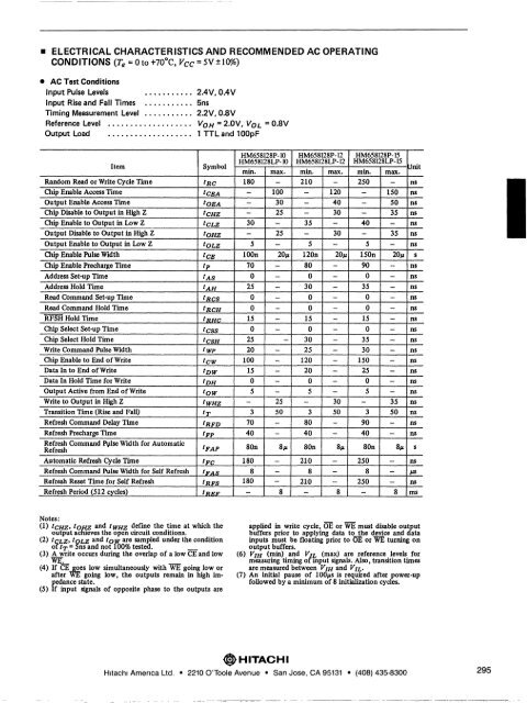
HM65256BLP-12 HM65256BLP-15 HM65256
- Page 11 and 12:
HB56A 18A1B-10 HB56A18A/B-12 HB56A1
- Page 14 and 15:
• PACKAGE INFORMATION .Dual-in-li
- Page 16 and 17:
---------------------------PACKAGE
- Page 18 and 19:
-----------------------------------
- Page 20 and 21:
f ---------------------------PACKAG
- Page 22 and 23:
• RELIABILITY OF HITACHI IC MEMOR
- Page 24 and 25:
-------------------------Rellablllt
- Page 26 and 27:
-------------------------Reliabilit
- Page 28 and 29:
--------------------------ReUablllt
- Page 30 and 31:
• PRECAUTIONS FOR HANDLING IC MEM
- Page 32 and 33:
~-~--- ~ -------- • QUALITY ASSUR
- Page 34 and 35:
--------------------------Quallty A
- Page 36 and 37:
------------ ----------------------
- Page 38 and 39:
• OUTLINE OF TESTING METHOD 1. IN
- Page 40 and 41:
----------------------------Outllne
- Page 42 and 43:
----------------------------Appllca
- Page 44 and 45:
----------------------------Program
- Page 46 and 47:
---------------------------Programm
- Page 48 and 49:
--------- • MASK ROM PROGRAMMING
- Page 50:
-- ------ -.. ---~~ Mask ROM Progra
- Page 53 and 54:
HM6148HP Series------- 1024-word' x
- Page 55 and 56:
HM6148HP Series -------------------
- Page 57 and 58:
HM6148HPSerles---------------------
- Page 59 and 60:
HM6148HLP Series------ 1024-word x
- Page 61 and 62:
HM6148HLPSeries -------------------
- Page 63 and 64:
HM6148HLPSeries -------------------
- Page 65 and 66:
HM6147HP Series -------------------
- Page 67 and 68:
HM6147HP Series -------------------
- Page 69 and 70:
HM6147HPSeries---------------------
- Page 71 and 72:
HM6147HLP Series ------------------
- Page 73 and 74:
HM6147HLP Series ------------------
- Page 75 and 76:
HM6116P Series---------------------
- Page 77 and 78:
HM6116P Series---------------------
- Page 79 and 80:
HM6116P Series---------------------
- Page 81 and 82:
HM6116FP Series -------------------
- Page 83 and 84:
HM6116FP Series -------------------
- Page 85 and 86:
HM6116LP Series 2048-word x 8-bit H
- Page 87 and 88:
HM6116LPSeries --------------------
- Page 89 and 90:
HM8116LPSerin----------------------
- Page 91 and 92:
HM6116LP Series--------------------
- Page 93 and 94:
HM6116LFP Series ---------- .TRUTH
- Page 95 and 96:
HM6116LFP Series eWRITE CYCLE (1) A
- Page 97 and 98:
HM6116AP Series, HM6116ASP Series -
- Page 99 and 100:
HM6116AP Series, HM6116ASP Series -
- Page 101 and 102:
HM6116AP Series, HM6116ASP Series -
- Page 103 and 104:
HM6116ALP Series,------ HM6116ALS
- Page 105 and 106:
HM6116ALP Series, HM6116ALSP Series
- Page 107 and 108:
HM6716 Series,-------Preliminary HM
- Page 109 and 110:
HM6716. HM6719 8erle8--------------
- Page 111 and 112:
HM6716, HM6719 Series--------------
- Page 113 and 114:
-~~------ __ ~ _____ -----___ " __
- Page 115 and 116:
HM6168HP Series -------------------
- Page 117 and 118:
HM6168HPSeries,--------------------
- Page 119 and 120:
HM6168HLP Series ------------------
- Page 121 and 122:
HM6168HLPSeries -------------------
- Page 123 and 124:
HM6268P Series-----Preliminary 4096
- Page 125 and 126:
HM6268P Series --------------------
- Page 127 and 128:
HM6268LP Series----Preliminary 4096
- Page 129 and 130:
HM6268LP Series -------------------
- Page 131 and 132:
-HM6268LPSeriM---------------------
- Page 133 and 134:
HM6167P Series --__________________
- Page 135 and 136:
HM6167PSeries ---------------------
- Page 137 and 138:
HM6167PSwie8 ______________________
- Page 139 and 140:
HM6167LP Series -------------------
- Page 141 and 142:
HM8187LPSeriH----------------------
- Page 143 and 144:
HM8187HP Series -TRUTH TABLE CS WE
- Page 145 and 146:
HM6167HP Series -------------------
- Page 147 and 148:
HM6167HPSMies----------------------
- Page 149 and 150:
HM6167HLP Series------ 16384-word x
- Page 151 and 152:
HM6167HLP Series -------------_____
- Page 153 and 154:
HM6267P Series 16384-word x '-bit H
- Page 155 and 156:
HM6267P Series eTIMING WAVEFORM OF
- Page 157 and 158:
HM6267P Series --------------------
- Page 159 and 160:
HM6267CG Series 16384-word x 1-bit
- Page 161 and 162:
HM6267CG Series -------------------
- Page 163 and 164:
HM6267LP Series 16384·word x 1·bi
- Page 165 and 166:
HM6267LP Series--------------------
- Page 167 and 168:
HM6267LP Series--------------------
- Page 169 and 170:
HM6264P Series --------------------
- Page 171 and 172:
HM6264P Series --------------------
- Page 173 and 174:
HM6264P Series --------------------
- Page 175 and 176:
HM6264FPSeries --------------------
- Page 177 and 178:
HM6264FP Series ___________________
- Page 179 and 180:
HM6264LP S.rl .. ------------------
- Page 181 and 182:
HM6264LP Series -------------------
- Page 183 and 184:
HM6264LP Series -----------________
- Page 185 and 186:
HM6264LFP Series------ 8192-word x
- Page 187 and 188:
HM6264LFP Series ------------------
- Page 189 and 190:
HM6264LFP Series __________________
- Page 191 and 192:
HM6264LP·LS.ies-------------------
- Page 193 and 194:
HM6264LP-L Series------------------
- Page 195 and 196:
HM6264LFP-L Series 8192-word x 8-bi
- Page 197 and 198:
HM6264LFP·L Series----------------
- Page 199 and 200:
HM6264LFP-L Series ---------_______
- Page 201 and 202:
HM6264ASP Series, HM6264AFP Series-
- Page 203 and 204:
HM6264ASP Series, HM6264AFP Series
- Page 205 and 206:
HM6264ASP Series, HM6264AFP Series-
- Page 207 and 208:
HM6264ALSP Series, HM6264ALFP Serie
- Page 209 and 210:
HM6264ALSP Serie., HM6264ALFP Serie
- Page 211 and 212:
HM6264ALSP Series. HM6264ALFP Serie
- Page 213 and 214:
HM6264ALSP Series, HM6264ALFP Serie
- Page 215 and 216:
HM6264LP-SL Series, HM6264LFP-SL Se
- Page 217 and 218:
HM6264LP-8L, HM6264LFP-sL Serle8---
- Page 219 and 220:
HM6264LP-SL, HM6264LFP-SL S8r18S---
- Page 221 and 222:
HM6288P Series---------------------
- Page 223 and 224:
HM6288P Series • Timing Waveform
- Page 225 and 226:
HM6788-----------------------------
- Page 227 and 228:
HM6788-----------------------------
- Page 229 and 230:
HM6287P Series, HM6287CG Series 655
- Page 231 and 232:
HM8287P Series, HM6287CG Series----
- Page 233 and 234:
HM6287P Series. HM6287CG Series----
- Page 235 and 236:
HM6287LP Series------- 65536-word X
- Page 237 and 238:
HM6287LP Series -------------------
- Page 239 and 240:
HM8287LPS.in-----------------------
- Page 241 and 242:
HM6787 Series, HM6787CG Series-----
- Page 243 and 244:
HMe787 Serl .. , HM6787CG SerI .. -
- Page 245 and 246:
HM62256LP Series,----- HM62256LFP
- Page 247 and 248:
HM822S8LP 8.,1 .., HM822S8LFP 8.,1
- Page 249 and 250:
HM62256LP Series, HM62256LFP Series
- Page 251 and 252:
HM62256LP Series, HM62256LFP Series
- Page 253 and 254:
HM62256LP Serlea, HM62256LFP Serlea
- Page 255 and 256:
HM62256LP-5L Series, HM62256LFP-5L
- Page 257 and 258: HM62256LP·SL Series, HM62256LFP·S
- Page 259 and 260: HM66202 Series NEW DESIGNS SHOULD U
- Page 261 and 262: HM662025erie5----------------------
- Page 263 and 264: HM66202 Series------------_________
- Page 265 and 266: HM66202L Series------- NEW DESIGNS
- Page 267 and 268: HM88202LS.le.----------------------
- Page 269 and 270: HM66202L Series-----------_________
- Page 271 and 272: HM66203 Series,------ HM66203L Se
- Page 273 and 274: HM66203-10/-12/-15, HM66203L-10/-12
- Page 275 and 276: HM66203-101-12/-15, HM66203L-10/-12
- Page 277 and 278: HM66204 Series,------ HM66204L Se
- Page 279 and 280: HM66204-121-15, HM66204L-12/-15----
- Page 281 and 282: HM66204-12/-15, HM66204L-12/-15 ---
- Page 283 and 284: 270
- Page 285 and 286: HM65256AP Series, HM65256ASP Series
- Page 287 and 288: HM85258AP SerI .. , HM85258ASPSerI
- Page 289 and 290: HM85258AP Serl .. , HM85258ASP Seri
- Page 291 and 292: HM65256AP Series, HM65256ASP Series
- Page 293 and 294: HM65256BP Series, HM65256BSP Series
- Page 295 and 296: HMe5258BP SerIes, HM85258BSP Series
- Page 297 and 298: HM65256BP Series, HM65256BSP Series
- Page 299 and 300: • 0 0 ••••• 0 0 0 0 0
- Page 301 and 302: HM85258BLP Seriea. HM85258BLSP Seri
- Page 303 and 304: HMe5258BLP Serf ... HM85258BLSP Ser
- Page 305 and 306: HM65256BLP Series. HM65256BLSP Seri
- Page 307: • TRUTH TABLE CE CS at CE going L
- Page 311 and 312: @HITACHI 298 Hitachi America Ltd .
- Page 313 and 314: HM50464P Series, HM50464CP Series 6
- Page 315 and 316: HM50464P Series, HM50464CP Serl88--
- Page 317 and 318: HM50464P Series, HM50464CP Series--
- Page 319 and 320: HM50484P Series. HM50484CP Series--
- Page 321 and 322: HM50465P Series, HM50465CP Series 6
- Page 323 and 324: HM50465P Series, HM50465CP Series--
- Page 325 and 326: HMS048SP Series, HMS048SCP Series--
- Page 327 and 328: HM50485P8eri .. , HM50485CP 8.rl ..
- Page 329 and 330: HM50256P Series, HM50256CP Series,
- Page 331 and 332: ~ 120 ~ 60 30 260 310 100 0 0 45 15
- Page 333 and 334: HM50256P Series. HM50256CP Series.
- Page 335 and 336: HM50256P Series, HM50256CP Series,
- Page 337 and 338: HM50257P Series, HM50257CP Series,
- Page 339 and 340: HM50257P Series. HM50257CP Series.
- Page 341 and 342: ---------------- HM50257P Series, H
- Page 343 and 344: HM50257P Serie., HM50257CP Serie.,
- Page 345 and 346: HM51256P Series-----Preliminary HM5
- Page 347 and 348: HM51256P Series, HM51256CP Series -
- Page 349 and 350: HM51256P Series. HM51256CP Series -
- Page 351 and 352: HM51258P Serl .. , HM51258CP Seri .
- Page 353 and 354: HM51256LP Series----Preliminary HM5
- Page 355 and 356: HM51256LP Series, HM51256LCP Series
- Page 357 and 358: HM51256lP Series. HM51256lCP Series
- Page 359 and 360:
HM51256LP Series, HM51256LCP Series
- Page 361 and 362:
HM51258P Series, HM51258CP Series 2
- Page 363 and 364:
HM51258P Series, HM51258CP Series -
- Page 365 and 366:
HM51258P Series, HM51258CP Series -
- Page 367 and 368:
HM51258P Series, HM51258CP Series -
- Page 369 and 370:
HM511000Series, HM511000P Series 10
- Page 371 and 372:
HM511000 Series, HM511000P Series -
- Page 373 and 374:
HM511000 Series, HM511000P Series--
- Page 375 and 376:
HM511000 Series. HM511000P Series--
- Page 377 and 378:
HM511000.JP-10/12/15 Series,---Prel
- Page 379 and 380:
HM511001 Series, HM511001P Series 1
- Page 381 and 382:
HM511001 8ari88, HM511001P 8.rl88--
- Page 383 and 384:
HM511001 Series. HM511001 P Series-
- Page 385 and 386:
HM511001 Series. HM511001 P Series-
- Page 387 and 388:
HM511001 Series, HM511001P Series--
- Page 389 and 390:
HM511002 Seri .. , HM511002P Series
- Page 391 and 392:
HM511002 Series, HM511002P Serles--
- Page 393 and 394:
HM511002 Serl .. , HM511002P Seri .
- Page 395 and 396:
HM511002 Series. HM511002P Series--
- Page 397 and 398:
~HITACHI 384 Hitachi America Ltd .
- Page 399 and 400:
HM53461P Series------ 65,536-word x
- Page 401 and 402:
HM53461PSeries---------------------
- Page 403 and 404:
HM53461PSeries---------------------
- Page 405 and 406:
HM53461PSeries---------------------
- Page 407 and 408:
HM53461PSeries---------------------
- Page 409 and 410:
HM53461 P Series ------------------
- Page 411 and 412:
HM53461P Sefies;-------------------
- Page 413 and 414:
HM53461PSeries---------------------
- Page 415 and 416:
HM53462P Series G5,53G-word x 4 bit
- Page 417 and 418:
HM53462P Series--------------------
- Page 419 and 420:
HM53462PSeries---------------------
- Page 421 and 422:
HM53462P Series--------------------
- Page 423 and 424:
HM53462PSeries---------------------
- Page 425 and 426:
HM53462P Series--------------------
- Page 427 and 428:
HM53462PSeries---------------------
- Page 429 and 430:
HM53462P Series--------------------
- Page 431 and 432:
HM53462PSeries---------------------
- Page 433 and 434:
HM53462P Series--------------------
- Page 435 and 436:
HM53462PSeries---------------------
- Page 437 and 438:
HM53462P Series--------------------
- Page 439 and 440:
HB561003A/B Series 282,144 x 9 bit
- Page 441 and 442:
HB561003A/B Series ----------------
- Page 443 and 444:
HB561003A1B Series-----------------
- Page 445 and 446:
HB561003A/BSeries------------------
- Page 447 and 448:
HB561003A1B Series-----------------
- Page 449 and 450:
HB56A 19A/B Series------Preliminary
- Page 451 and 452:
HB561008BSeries--------------------
- Page 453 and 454:
HB561008BS.ies---------------------
- Page 455 and 456:
HB561008B Series-------------------
- Page 457 and 458:
HB561008BSeries-----------------;--
- Page 459 and 460:
HN61364P, HN61364FP 8192-word x 8-b
- Page 461 and 462:
HN61365P 8192-word x 8-bit CMOS Mas
- Page 463 and 464:
HN61366P 8192-word x 8-bit CMOS Mas
- Page 465 and 466:
HN613128P, HN613128FP 16384-word x
- Page 467 and 468:
HN61256P, HN61256FP 32768X8-blt or
- Page 469 and 470:
HN613256P, HN613256FP 32768·word x
- Page 471 and 472:
HN623256~HN623256FP 32678-word X 8-
- Page 473 and 474:
HN62301AP, HN62301AFP 131,072-word
- Page 475 and 476:
HN62301AP,HN62301AFP---------------
- Page 477 and 478:
HN62301BP,HN62301BFP---------------
- Page 479 and 480:
HN62301DP HN62301DFP Preliminary 13
- Page 481 and 482:
HN62301DP,HN62301DFP---------------
- Page 483 and 484:
HN62402P---------------------------
- Page 485 and 486:
HN62302P 262,144 x 8 bit CMOS Mask
- Page 487 and 488:
HN62302P---------------------------
- Page 489 and 490:
HN27C64G Series 8192-word x 8-bit U
- Page 491 and 492:
HN27C64G Series -------------------
- Page 493 and 494:
HN27C64G Series--------------------
- Page 495 and 496:
HN27C64G Series -------------------
- Page 497 and 498:
HN27C64FP Series-------------------
- Page 499 and 500:
HN27C64FPSeries--------------------
- Page 501 and 502:
HN27128AG Series------- 16384-word
- Page 503 and 504:
HN27128AG Series-------------------
- Page 505 and 506:
HN27128AG S.rl88-------------------
- Page 507 and 508:
HN27128AG Series-------------------
- Page 509 and 510:
HN27128APSeries--------------------
- Page 511 and 512:
HN27128AP Series ------------------
- Page 513 and 514:
HN27128AP Series-------------------
- Page 515 and 516:
HN27256GSeries---------------------
- Page 517 and 518:
HN27256G Series--------------------
- Page 519 and 520:
HN2?256P Series Preliminary 32768-w
- Page 521 and 522:
HN27256P Serie8--------------------
- Page 523 and 524:
HN27C256G Series 32768-word x 8-bit
- Page 525 and 526:
HN27C256GS.ies---------------------
- Page 527 and 528:
HN27C256G Series------------~------
- Page 529 and 530:
HN27C256FP Series------ 32768-word
- Page 531 and 532:
HN27C258FP-------------------------
- Page 533 and 534:
HN27C256FP-------------------------
- Page 535 and 536:
HN27512G Series • MODE SELECTION
- Page 537 and 538:
HN27512GSeri.,---------------------
- Page 539 and 540:
HN27512G Series--------------------
- Page 541 and 542:
HN27612P Series-----Preliminary 656
- Page 543 and 544:
HN27512P Series -------------------
- Page 545 and 546:
HN27512PSerles---------------------
- Page 547 and 548:
HN27C1024G Series-Under Development
- Page 549 and 550:
HN27C101G~-------------------------
- Page 551 and 552:
HN27C101GS«ieB--------------------
- Page 553 and 554:
HN27C101G Serl88-------------------
- Page 555 and 556:
HN27C301G Series----Preliminary 131
- Page 557 and 558:
HN27C301G Series-------------------
- Page 559 and 560:
HN27C301G Series-------------------
- Page 561 and 562:
~ 2 HN27C301G Series --------------
- Page 563 and 564:
HN58064P Series------- 8192·word x
- Page 565 and 566:
HN58064PSMies----------------------
- Page 567 and 568:
HN58064PSeries---------------------
- Page 569 and 570:
HN58C65P Series ----Preliminary 819
- Page 571 and 572:
HN58C85P Serles--------------------
- Page 573 and 574:
HN58C85PSenH-----------------------
- Page 575 and 576:
HN58C65PS.le8----------------------
- Page 577 and 578:
564
- Page 579 and 580:
HM10414, HM10414-1------ 256-word x
- Page 581 and 582:
HM10414,HM10414-1------------------
- Page 583 and 584:
HM10422 256-word x 4-bit Fully Deco
- Page 585 and 586:
HM10422----------------------------
- Page 587 and 588:
HM10422----------------------------
- Page 589 and 590:
HM10422·7-------------------------
- Page 591 and 592:
HM2110, HM2110-1 1 024-word x 1-bit
- Page 593 and 594:
HM211~HM2110-1---------------------
- Page 595 and 596:
HM2112, HM2112-1 1 024-word x 1-bit
- Page 597 and 598:
HM2112,HM2112-1--------------------
- Page 599 and 600:
HM2112,HM2112-1--------------------
- Page 601 and 602:
~74--------------------------------
- Page 603 and 604:
HM~74------------------------------
- Page 605 and 606:
HM10474-S,HM10474-10 1024-wordX4-bl
- Page 607 and 608:
HM10474-8,HM10474-10---------------
- Page 609 and 610:
HM10470,HM10470.1------------------
- Page 611 and 612:
HM1047~HM10470·1------------------
- Page 613 and 614:
HM10480,HM10480F 16,384-words x 1-b
- Page 615 and 616:
HM1~.HM1~--------------------------
- Page 617 and 618:
HM10480-15.HM10480F-15-------------
- Page 619 and 620:
HM10480L 16,384-words X 1-bit Fully
- Page 621 and 622:
HM10480L---------------------------
- Page 623 and 624:
HM100422,HM100422F,HM100422CG------
- Page 625 and 626:
HM100415,HM100415CG 1024-word x 1-b
- Page 627 and 628:
HM100415,HM100415CG----------------
- Page 629 and 630:
HM100474.HM100474F-----------------
- Page 631 and 632:
HM100474,HM100474F-----------------
- Page 633 and 634:
HM100474-8,HM100474-10Prellmlnary H
- Page 635 and 636:
HM100474-8, HM1 00474-1 0, HM100474
- Page 637 and 638:
HM100470---------------------------
- Page 639 and 640:
HM1 00480-15, -------Preliminary HM
- Page 641 and 642:
HM100480-15,HM100480F-15,----------
- Page 643:
NOTES