P1149.7 - Board Test Workshop Home Page
P1149.7 - Board Test Workshop Home Page
P1149.7 - Board Test Workshop Home Page

You also want an ePaper? Increase the reach of your titles
YUMPU automatically turns print PDFs into web optimized ePapers that Google loves.
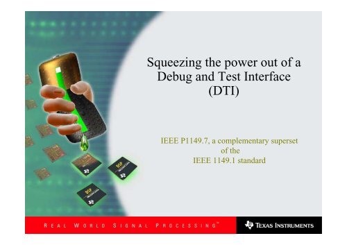
Squeezing the power out of a<br />
Debug and <strong>Test</strong> Interface<br />
(DTI)<br />
IEEE <strong>P1149.7</strong>, a complementary superset<br />
of the<br />
IEEE 1149.1 standard<br />
GS - BTW - 09/014/2006
<strong>P1149.7</strong><br />
An introduction to the proposed standard<br />
Gary Swoboda<br />
TI Fellow, Texas Instruments<br />
System Architect, CTO / Debug Architecture<br />
September 14, 2006<br />
Ft. Collins, Colo./BTW06<br />
2
Presentation Outline<br />
<strong>P1149.7</strong> history and status<br />
Why 1149.7?<br />
What can it do?<br />
What about performance?<br />
How does it work?<br />
How is it deployed?<br />
3
1149.1 and <strong>P1149.7</strong><br />
What is their relationship?<br />
<strong>P1149.7</strong> is not a replacement for 1149.1<br />
<strong>P1149.7</strong> uses 1149.1 as its foundation<br />
<strong>P1149.7</strong> provides 1149.1 extensions<br />
<strong>P1149.7</strong> provides 2-pin operating modes<br />
GS - BTW - 09/014/2006
<strong>P1149.7</strong> History and Status<br />
MIPI Origins<br />
Objective – define a backwards compatible minimum pin debug interface<br />
Strategy – requirements gathering, technical debate<br />
Tactics – solicit competing proposals, choose a winner<br />
Result – <strong>P1149.7</strong> was handily selected as winning proposal vs. SWD<br />
Collaboration with Nexus consortium<br />
Objective – Compare common needs, explore common solution<br />
Strategy - Joint meetings, compare requirements<br />
Tactics - Specifications reviewed, incorporate feedback<br />
Result – Agreement to pursue IEEE standard because of large field of use<br />
IEEE PAR approved<br />
<strong>Test</strong>, Debug, and backwards IEEE 1149.1 compatibility considerations<br />
Specification reviewed and revision underway<br />
Presumed Result – IEEE 1149.7 standard in early 2007<br />
GS - BTW - 09/014/2006
Why <strong>P1149.7</strong>?<br />
Harness 1149.1 entropy and provide a<br />
framework for creativity<br />
Addresses multiple on-chip TAP controllers<br />
Serves both applications debug and test needs<br />
More functions supporting applications debug<br />
Applications instrumentation over the same pins used for test<br />
GS - BTW - 09/014/2006
Engage Consortiums:<br />
<strong>P1149.7</strong> Activity<br />
MIPI<br />
Nexus<br />
OCP<br />
Engage Strategic Companies<br />
Silicon, Tools and <strong>Test</strong>:<br />
• North America - Intel, Freescale, Xilinx, Corelis, EWA, etc.<br />
• Europe - STM, Philips, Nokia, Lauterbach, etc.<br />
• Asia - NEC, Fujitsu, Toshiba, Sophia, YDC, etc.<br />
Engage “the Masses”<br />
IEEE 1149.7<br />
GS - BTW - 09/014/2006
Standards Focus<br />
1149.1 vs. <strong>P1149.7</strong><br />
1149.1 <strong>P1149.7</strong><br />
<strong>Test</strong><br />
Boundary Scan:<br />
Finding card level<br />
connectivity issues<br />
Compliance: Preserving<br />
boundary scan for System<br />
on a Chip (SoC)<br />
Apps<br />
Capability: Features for<br />
debug<br />
GS - BTW - 09/014/2006
Key <strong>P1149.7</strong> Objectives<br />
Do more with less<br />
• Operate with fewer pins<br />
• Add instrumentation using the same pins<br />
• TAP power management<br />
• Provide framework for diverse debug technologies<br />
• Preserve gateway to debug of SI errors/defects<br />
Preserve industry investment<br />
•SI IP<br />
• Software IP<br />
• Debug and <strong>Test</strong> Tools<br />
Provide means for innovation/customization<br />
• Pin protocols other than those supporting scan<br />
• Mix and match legacy/new IP<br />
• Equal treatment for all industry IP<br />
GS - BTW - 09/014/2006
Applications Debug Forces at Work<br />
“Hold test gains while achieving better pin utilization”<br />
Debug + <strong>Test</strong> >><br />
“Make the right compromises”<br />
Custom protocols supported<br />
Instrument application<br />
Preserve scan performance<br />
Reduce pin count for test/debug<br />
Preserve <strong>Test</strong> IP, localize change<br />
Preserve SW IP, localize change<br />
Manage pin utilization in a structured way<br />
Scan and instrumentation packets<br />
Less pins/same performance<br />
More functions on test pins<br />
1149.1 fundamentals preserved<br />
Selection layer only<br />
Allow use of existing test equipment<br />
Preserve SI IP, minimize change<br />
Protocol converter<br />
1149.1 foundation<br />
GS - BTW - 09/014/2006
GS - BTW - 09/014/2006<br />
So, what can it do?
<strong>P1149.7</strong> – A Debug and <strong>Test</strong> Tech. Binder<br />
“All industry IP co-exists behind a standard Interface”<br />
Standard interface<br />
benefits tools<br />
suppliers and users<br />
Standard<br />
1149.1<br />
Functions<br />
Boundary Scan<br />
Chip TAPs<br />
Narrow (2)<br />
or<br />
Wide (4)<br />
<strong>P1149.7</strong><br />
Controller<br />
BDX<br />
CDX<br />
Instrumentation Sources<br />
BDM (Freescale)/<br />
SWD (ARM)/other<br />
Power<br />
Chip Power and Reset<br />
Controller<br />
<strong>Test</strong><br />
<strong>Test</strong> and Private<br />
Interface Modes<br />
<br />
<br />
Signaling is 1149.1 at start-up<br />
SW directed mode switches between use of<br />
standard and advanced protocol<br />
<br />
<br />
Once interface mode is set, software drivers<br />
communicate with standard 1149.1 protocol<br />
SW controls transmission efficiency by selection of<br />
transmission format best suiting system characteristics<br />
GS - BTW - 09/014/2006
Scan<br />
BDX<br />
CDX<br />
Power<br />
<strong>Test</strong><br />
A Look Inside <strong>P1149.7</strong><br />
“Major functions”<br />
Optimized serialization of<br />
nTRST, TMS, TDI, and TDO<br />
Pause and Idle states provide<br />
instrumentation channel<br />
Shift_DR state may be used to<br />
overlay any custom protocol<br />
Chip power and reset controller<br />
managing interface power<br />
<strong>Test</strong> and private<br />
interface modes<br />
Multiple formats<br />
Pin<br />
BW Utilization<br />
Extensibility<br />
Every microwatt<br />
counts<br />
Specialty<br />
Deployment Profile<br />
Minimal Moderate Most<br />
Flash, CPLDs,<br />
FPGAs<br />
SOC or<br />
Micro-Controller<br />
Sophisticated<br />
SOC<br />
GS - BTW - 09/014/2006
BDX – Better Use of Link BW<br />
“The Compound 80/20 Rule of Interface Activity”<br />
~80% of time is spent<br />
between actions<br />
~80% of operating time<br />
spend doing an action is in parked<br />
states (IDLE, Pause_DR, Pause_IR)<br />
~20% of time is spent<br />
using the link<br />
~20% of operating time is<br />
spent doing useful work<br />
Full link BW is needed for control ~ 4% of the time<br />
Use Idle Control Periods for Background Data Exchange (BDX )<br />
GS - BTW - 09/014/2006
CDX – Custom Use of Link BW<br />
“Supports vendor specific protocols”<br />
• Redirects activity during Shift_DR states<br />
• All controllers do not need to understand protocol<br />
• Only device that is selected for scan participates<br />
• DTS or Device may be master<br />
• Different CDX formats may be TDMed<br />
• Entirely under software control<br />
• Can be invoked “inline” with scans<br />
Full link BW is provide to any function<br />
CDX follows BDX rules set only CDX manages line direction each bit<br />
GS - BTW - 09/014/2006
So, what about performance?<br />
GS - BTW - 09/014/2006
<strong>P1149.7</strong> – Adds capability to 1149.1<br />
“Minimizing Changes/Maintaining Performance”<br />
• The same or better than IEEE1149.1 may be achieved in some cases<br />
• With advanced protocol<br />
• Falling–edge to falling edge timing allows doubling TCK rate<br />
• The amount of information transferred is minimized to boost performance<br />
• Two or less bits are transferred/TAP controller state in some cases<br />
2 bits/TAP state/ 2*TCK rate = the same TCK/TAP state rate as IEEE 1149.1<br />
20 MHz 40 MHz<br />
20 MHz<br />
Existing<br />
controller<br />
Emulator<br />
adapter<br />
logic<br />
Chip<br />
adapter<br />
logic<br />
Existing<br />
Si IP<br />
<br />
<br />
<strong>P1149.7</strong> added<br />
May be added to existing controller<br />
Narrow (2-pins)<br />
or<br />
Wide (4-pins)<br />
<br />
<br />
<strong>P1149.7</strong> added<br />
No changes to existing Si IP<br />
GS - BTW - 09/014/2006
GS - BTW - 09/014/2006<br />
So, how does it work?
<strong>P1149.7</strong> Overview<br />
Extensions to the IEEE 1149.1 protocol<br />
Mobile<br />
Telecom<br />
4-pin<br />
• Adds additional levels of control hierarchy<br />
• Firewall and Super Bypass TM bit tackle series scan path length and<br />
system corruption with DTS and TS physical connect/disconnect<br />
Video<br />
Existing<br />
DTS<br />
New capability added with IEEE <strong>P1149.7</strong><br />
4<br />
Chip<br />
TAPs<br />
Mobile<br />
Video<br />
Telecom<br />
• 80 - 100 MHz operation<br />
• 1 or 2 Pins<br />
• Combined scan/instrumentation/custom use of pins<br />
• Glueless Interface to Multiple Devices (16 per DTS Port)<br />
2/4 pin<br />
Existing<br />
DTS<br />
DTS<br />
Adapter<br />
<strong>P1149.7</strong> Bridge<br />
2<br />
4<br />
TS<br />
Adapter<br />
Chip<br />
TAPs<br />
GS - BTW - 09/014/2006
Connection Topologies<br />
2-pin Star Scan Topology<br />
When all chips have<br />
Class 3 or Class 4 TAPs<br />
the 4-pin topologies<br />
may be operated as a<br />
2-pin topology<br />
DTC<br />
Interface<br />
TCK<br />
TMS<br />
T<br />
C<br />
K<br />
T<br />
M<br />
S<br />
TCK<br />
TMS<br />
T<br />
C<br />
K<br />
T<br />
M<br />
S<br />
GS - BTW - 09/014/2006
Harmony with the 1149.1 Standard<br />
TMS becomes Bi-directional in 2-pin modes<br />
• TMS renamed TMSC<br />
• Drive while TCK low, Hi-z while TCK high<br />
• Data sampling programmable (TCK , TCK )<br />
• Always HI-z when TCK high<br />
• Also used for Link Reset<br />
SW Same IP<br />
Infrastructure<br />
Remains<br />
TMSC toggling while TCK high<br />
• 6 edges - while Link Reset<br />
• 2/3 edges – escape data transmission (extra cntl.)<br />
Same Drivers<br />
Virtually<br />
4-pin Star<br />
• Looks like 2-pin with TDI/TDO added<br />
• Parallel addressability works the same as 2-pin<br />
• All initialization works the same<br />
Plug Untouched and Play<br />
Configuration<br />
4-pin Series<br />
• Looks like 2-pin with series TDI/TDO added<br />
• Parallel addressability/initialization works the same<br />
• Parallel (Star) and Series Addressing (Super Bypass TM )<br />
(except for TAP selection layer)<br />
2- pin<br />
Star<br />
TCK<br />
TMSC<br />
4 - pin<br />
Star<br />
TCK<br />
TMSC<br />
TDI<br />
TDO<br />
4 - pin<br />
Series<br />
TCK<br />
TMSC<br />
TDI<br />
TDO<br />
TI<br />
Mobile<br />
TI<br />
Mobile<br />
TI<br />
Mobile<br />
TI<br />
Video<br />
2-pin Star<br />
+<br />
TI<br />
Video<br />
4-pin Star<br />
+<br />
TI<br />
Video<br />
TI<br />
Telecom<br />
TI<br />
Telecom<br />
TI<br />
Telecom<br />
4-pin Series<br />
GS - BTW - 09/014/2006
Key Control Concepts<br />
Extend functionality of BYPASS and IDCODE instructions<br />
(“overload” these instructions)<br />
Keep new command structure invisible to existing 1149.1 TAPs<br />
Create commands without using TDI or TDO<br />
Use commands to create registers without changing IR/DR scan paths<br />
GS - BTW - 09/014/2006
Overloading the Bypass Instruction<br />
(using Zero-bit DR-Scans (ZBS))<br />
• IR register set to BYPASS or IDCODE<br />
instruction by:<br />
• IR-Scan or<br />
• <strong>Test</strong>-Logic-Reset<br />
Method:<br />
• ZBS = CaptureExitUpdate<br />
• The number of consecutive ZBSs are counted<br />
to create a control level that specifies the<br />
overloaded function<br />
• This is performed by standard IEEE 1149.1<br />
TAP controller state sequences<br />
IR Register<br />
BYPASS<br />
GS - BTW - 09/014/2006
Zero-Bit Scans Create Control Levels<br />
Key:<br />
1….<br />
2….<br />
3….<br />
Lock Control<br />
Level at 3.<br />
IR Register<br />
BYPASS<br />
• Count the<br />
number of Zero-<br />
Bit-Scans (ZBS) to<br />
change the<br />
definition of<br />
BYPASS<br />
instruction.<br />
• Lock control level<br />
when the Shift-DR<br />
state is reached.<br />
GS - BTW - 09/014/2006
Creating a Control Level<br />
Example: Steps to create a control level 3<br />
1. IR-Scan with BYPASS instr.<br />
2. ZBS<br />
3. ZBS<br />
4. ZBS<br />
Example: Steps to create a control level 5<br />
1. IR-Scan with BYPASS instr.<br />
2. ZBS<br />
3. ZBS<br />
4. ZBS<br />
5. ZBS<br />
6. ZBS<br />
BYPASS instruction<br />
Increment control level from 0 to 1<br />
Increment control level from 1 to 2<br />
Increment control level from 2 to 3<br />
BYPASS instruction<br />
Increment control level from 0 to 1<br />
Increment control level from 1 to 2<br />
Increment control level from 2 to 3<br />
Increment control level from 3 to 4<br />
Increment control level from 4 to 5<br />
GS - BTW - 09/014/2006
Extending 1149.1<br />
Pins Required=4<br />
Required=2<br />
Core<br />
A<br />
Core<br />
B<br />
SW Driver<br />
TDI<br />
TMS<br />
TCLK<br />
TDO<br />
EMU0<br />
EMU1<br />
TDI<br />
TMS<br />
TCLK<br />
TDO<br />
EMU0<br />
EMU1<br />
TCLK<br />
TCLK<br />
TCLK<br />
TMS<br />
TMS<br />
0xcoffee<br />
TMSC<br />
Emulator<br />
TDI<br />
TDO<br />
EMU0<br />
TDI<br />
TDO<br />
EMU0<br />
0xcoffee<br />
TDI<br />
TDO<br />
EMU0<br />
EMU1<br />
EMU1<br />
EMU1<br />
Mode=Advanced<br />
•EMU0 and EMU1 are typically used for to gather large<br />
amounts communication with a target application<br />
•Using Background Data eXchange (BDX) and Custom<br />
Data eXchange (CDX), target information can be<br />
transferred.<br />
•For maximum compatibility, CDX can be used to carry<br />
manufacturer defined protocols.<br />
GS - BTW - 09/014/2006
Extending 1149.1<br />
Pins Required=2<br />
Core<br />
A<br />
Core<br />
B<br />
SW Driver<br />
TDI<br />
TMS<br />
TCLK<br />
TDO<br />
EMU0<br />
EMU1<br />
TDI<br />
TMS<br />
TCLK<br />
TDO<br />
EMU0<br />
EMU1<br />
Emulator<br />
TCLK<br />
TMSC<br />
TDI<br />
TDO<br />
EMU0<br />
TCLK<br />
TMSC<br />
TDI<br />
TDO<br />
EMU0<br />
EMU1<br />
Mode=Advanced<br />
EMU1<br />
GS - BTW - 09/014/2006
GS - BTW - 09/014/2006<br />
How is it deployed?
<strong>P1149.7</strong> Deployment Method<br />
Capability classes:<br />
3 classes - 4-pin using IEEE 1149.1 protocol<br />
2 classes - 2/4-pin using IEEE 1149.1 protocol<br />
GS - BTW - 09/014/2006
<strong>P1149.7</strong> “Classes”<br />
Deliver:<br />
a) 1149.1 extensions with standard protocol<br />
b) 2-pin operation with advanced protocol<br />
c) Bi-modal operation with plug and play<br />
With five classes of capability:<br />
Class T0 – IEEE Compliance for chips with multiple TAPs<br />
Class T1 – Add control functions/preserving IP (e.g. chip reset(s))<br />
Class T2 – Add chip selection for series and star configurations<br />
Class T3 – Add two pin operation<br />
Class T4 – Add instruction/custom pin use to two pin operation<br />
GS - BTW - 09/014/2006
IEEE <strong>P1149.7</strong> Class Details<br />
Class T0<br />
Class T1<br />
Class T2<br />
Class T3<br />
Class T4<br />
• Ensure compliance with 1149.1 to<br />
enhance compatibility with industry<br />
test infrastructure<br />
• Power: <strong>Test</strong> logic power-down<br />
•Performance:<br />
•Shortened multi-chip scan<br />
chains<br />
•Glue-less star configuration<br />
• Pins: Less pin and more functions<br />
•Faster downloads to target<br />
•Equivalent performance with<br />
fewer pins<br />
• Instrumentation<br />
• Customization<br />
• After <strong>Test</strong>-Logic-Reset (TLR) multi-TAP devices:<br />
•Conform to mandatory 1149.1 instruction<br />
behavior<br />
•1-bit DR-Scan for bypass instruction<br />
• Addresses stacked die and multi-chip module needs<br />
• 4 Power Down modes friendly to: <strong>Board</strong> <strong>Test</strong>,<br />
Chip <strong>Test</strong>, and Application Debug<br />
•Chip Level Bypass<br />
• Built-in Chip Select Mechanism<br />
• 2 pins provide scan, <strong>Test</strong>-Logic-Reset (TLR), and<br />
instrumentation (serialized transactions)<br />
• Download specific modes (Target Input only)<br />
• 2x Clock rate and optimized transactions<br />
• Concurrent Debug and Instrumentation using<br />
same pins<br />
• Instrumentation of data passed during Run-<strong>Test</strong>-<br />
Idle, Pause-DR, and Pause-IR states<br />
• Custom technologies can use the test access port<br />
pins in Shift-DR state. (ex: SWD, BDM, etc. )<br />
Higher numbered classes operate with lower numbered classes<br />
GS - BTW - 09/014/2006
How will <strong>P1149.7</strong> be used?<br />
Class T0/T1 – any system, mix/match with 1149.1<br />
Class T2<br />
• Series topology - Mix/match with 1149.1 devices<br />
• Star topology - Match with 1149.7 Class 2<br />
Class T3/T4 – (4-pin)<br />
• Series topology - Mix/match with 1149.1, T0, T1, and T2 devices<br />
• Series topology - Mix/match with T3/T4 devices, operate as 2-pin<br />
• Star topology – Mix/match with T2 supporting Star, T3/T4<br />
Class T3/T4 – (2-pin) – Mix/match with T3/T4 devices:<br />
1149.1 and 2-pin T3/T4 devices may share either TCK or<br />
TMSC but not both if they are used together. The 2-pin and<br />
4-pin interfaces may be also be kept separate.<br />
GS - BTW - 09/014/2006
Projected adoption profile<br />
Class 0:<br />
• Should be no barriers<br />
Class 1:<br />
• Systems with embedded cores/application dev. needs<br />
• Some FPGAs<br />
Class 2 :<br />
• Systems with large number of chips<br />
• Systems with embedded cores/application dev. needs<br />
Class T3/T4 – (4-pin) :<br />
• Mass market devices that may be mixed with T3/T4 chips in system<br />
• Systems with applications development needs<br />
Class T3/T4 – (2-pin):<br />
• Wireless handheld devices<br />
• Consumer products<br />
GS - BTW - 09/014/2006
Where does <strong>P1149.7</strong> take us?<br />
Here are the choices >><br />
1149.1 <strong>Test</strong> and Debug<br />
Overlap<br />
1149.7 <strong>Test</strong> and Debug<br />
Overlap<br />
<strong>Test</strong> – easier<br />
Debug - harder<br />
<strong>Test</strong> – a bit slower<br />
Debug - easier<br />
GS - BTW - 09/014/2006