Semiconductor Avalanche Diode Detectors for Quantum Cryptography
Semiconductor Avalanche Diode Detectors for Quantum Cryptography
Semiconductor Avalanche Diode Detectors for Quantum Cryptography

You also want an ePaper? Increase the reach of your titles
YUMPU automatically turns print PDFs into web optimized ePapers that Google loves.
20leos05.qxd 10/5/06 2:15 PM Page 20<br />
<strong>Semiconductor</strong> <strong>Avalanche</strong> <strong>Diode</strong> <strong>Detectors</strong><br />
<strong>for</strong> <strong>Quantum</strong> <strong>Cryptography</strong><br />
Gerald S Buller, Sara Pellegrini, Ryan E. Warburton, Jo Shien Ng*, Lionel JJ Tan*,<br />
Andrey Krysa*, John P.R. David* and Sergio Cova+<br />
Abstract<br />
Advances in semiconductor single photon avalanche diode<br />
detectors have enabled an expansion in photon-counting<br />
application areas in the near-infrared. Of particular relevance<br />
is the application area of quantum key distribution<br />
in which secure encryption keys can be shared between<br />
users using in<strong>for</strong>mation derived from streams of encoded<br />
single-photons. We report progress towards the objective<br />
of a practical, high efficiency detector at the strategically<br />
important 1550nm wavelength band.<br />
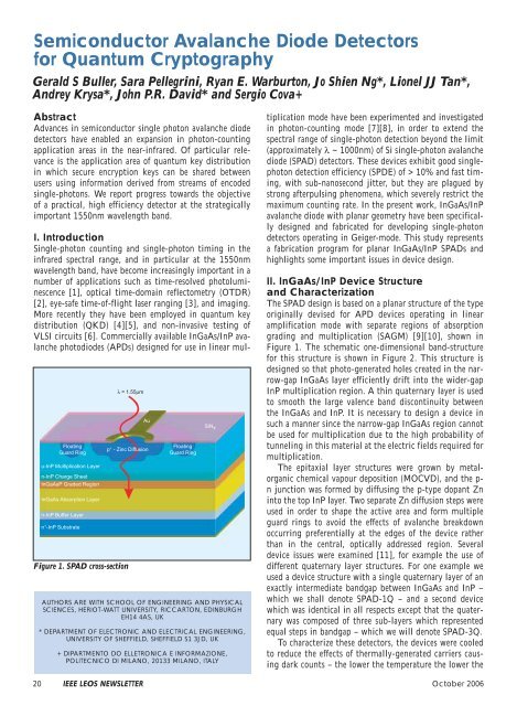
Floating<br />
Guard Ring<br />
u-InP Multiplication Layer<br />
n-InP Charge Sheet<br />
InGaAsP Graded Region<br />
InGaAs Absorption Layer<br />
n-InP Buffer Layer<br />
n + -InP Substrate<br />
λ = 1.55μm<br />
Floating<br />
Guard Ring<br />
SiNx<br />
AUTHORS ARE WITH SCHOOL OF ENGINEERING AND PHYSICAL<br />
SCIENCES, HERIOT-WATT UNIVERSITY, RICCARTON, EDINBURGH<br />
EH14 4AS, UK<br />
* DEPARTMENT OF ELECTRONIC AND ELECTRICAL ENGINEERING,<br />
UNIVERSITY OF SHEFFIELD, SHEFFIELD S1 3JD, UK<br />
+ DIPARTMENTO DO ELLETRONICA E INFORMAZIONE,<br />
POLITECNICO DI MILANO, 20133 MILANO, ITALY<br />
Au<br />
p + - Zinc Diffusion<br />
Figure 1. SPAD cross-section<br />
I. Introduction<br />
Single-photon counting and single-photon timing in the<br />
infrared spectral range, and in particular at the 1550nm<br />
wavelength band, have become increasingly important in a<br />
number of applications such as time-resolved photoluminescence<br />
[1], optical time-domain reflectometry (OTDR)<br />
[2], eye-safe time-of-flight laser ranging [3], and imaging.<br />
More recently they have been employed in quantum key<br />
distribution (QKD) [4][5], and non-invasive testing of<br />
VLSI circuits [6]. Commercially available InGaAs/InP avalanche<br />
photodiodes (APDs) designed <strong>for</strong> use in linear multiplication<br />
mode have been experimented and investigated<br />
in photon-counting mode [7][8], in order to extend the<br />
spectral range of single-photon detection beyond the limit<br />
(approximately λ ~ 1000nm) of Si single-photon avalanche<br />
diode (SPAD) detectors. These devices exhibit good singlephoton<br />
detection efficiency (SPDE) of > 10% and fast timing,<br />
with sub-nanosecond jitter, but they are plagued by<br />
strong afterpulsing phenomena, which severely restrict the<br />
maximum counting rate. In the present work, InGaAs/InP<br />
avalanche diode with planar geometry have been specifically<br />
designed and fabricated <strong>for</strong> developing single-photon<br />
detectors operating in Geiger-mode. This study represents<br />
a fabrication program <strong>for</strong> planar InGaAs/InP SPADs and<br />
highlights some important issues in device design.<br />
II. InGaAs/InP Device Structure<br />
and Characterization<br />
The SPAD design is based on a planar structure of the type<br />
originally devised <strong>for</strong> APD devices operating in linear<br />
amplification mode with separate regions of absorption<br />
grading and multiplication (SAGM) [9][10], shown in<br />
Figure 1. The schematic one-dimensional band-structure<br />
<strong>for</strong> this structure is shown in Figure 2. This structure is<br />
designed so that photo-generated holes created in the narrow-gap<br />
InGaAs layer efficiently drift into the wider-gap<br />
InP multiplication region. A thin quaternary layer is used<br />
to smooth the large valence band discontinuity between<br />
the InGaAs and InP. It is necessary to design a device in<br />
such a manner since the narrow-gap InGaAs region cannot<br />
be used <strong>for</strong> multiplication due to the high probability of<br />
tunneling in this material at the electric fields required <strong>for</strong><br />
multiplication.<br />
The epitaxial layer structures were grown by metalorganic<br />
chemical vapour deposition (MOCVD), and the p-<br />
n junction was <strong>for</strong>med by diffusing the p-type dopant Zn<br />
into the top InP layer. Two separate Zn diffusion steps were<br />
used in order to shape the active area and <strong>for</strong>m multiple<br />
guard rings to avoid the effects of avalanche breakdown<br />
occurring preferentially at the edges of the device rather<br />
than in the central, optically addressed region. Several<br />
device issues were examined [11], <strong>for</strong> example the use of<br />
different quaternary layer structures. For one example we<br />
used a device structure with a single quaternary layer of an<br />
exactly intermediate bandgap between InGaAs and InP –<br />
which we shall denote SPAD-1Q – and a second device<br />
which was identical in all respects except that the quaternary<br />
was composed of three sub-layers which represented<br />
equal steps in bandgap – which we will denote SPAD-3Q.<br />
To characterize these detectors, the devices were cooled<br />
to reduce the effects of thermally-generated carriers causing<br />
dark counts – the lower the temperature the lower the<br />
20 IEEE LEOS NEWSLETTER October 2006
20leos05.qxd 10/5/06 2:15 PM Page 21<br />
www.i-leos.org<br />
Eldorado Hotel, Santa Fe, New Mexico<br />
18th Annual Workshop on<br />
Interconnections Within<br />
High Speed Digital Systems<br />
20-23 May 2007<br />
Sponsored by the IEEE Lasers & Electro-Optics Society<br />
and in cooperation with the IEEE Computer Society<br />
Photo: Jack Parsons<br />
REGISTRATION DEADLINE: 23 APRIL 2007
20leos05.qxd 10/5/06 2:15 PM Page 22<br />
dark count rate within the devices. It was also necessary to<br />
electrically gate the detectors, so that they operated above<br />
the avalanche breakdown point – the so-called Geiger<br />
mode – only <strong>for</strong> a short period around the expected photon<br />
arrival time.<br />
Figure 3 shows the single-photon detection efficiency<br />
and dark count rates of these detectors as a function of<br />
temperature <strong>for</strong> similar detector overbias levels. It is particularly<br />
evident that there is a large improvement in<br />
detection efficiency with the “stepped” quaternary layer.<br />
Figure 4 illustrates the jitter as a function of overbias,<br />
described in terms of a full-width at half maximum, <strong>for</strong><br />
the SPAD 3Q device fabricated in different device diameters.<br />
It is also evident that the detectors have the potential<br />
of timing at a level consistent with GHz clocking in a<br />
Energy<br />
hυ<br />
p + InP<br />
n − InP<br />
Band Structure<br />
n + InP<br />
InGaAsP<br />
e −<br />
−<br />
+<br />
h +<br />
n InGaAs<br />
Vrev<br />
Depth<br />
Figure 2. Schematic energy band-structure of InGaAs/InP SPAD<br />
quantum key distribution application. The expected<br />
device diameter dependence of the jitter is due to the lateral<br />
spreading of the avalanche during build-up across the<br />
full device diameter.<br />
In terms of device sensitivity, one figure of merit is noise<br />
equivalent power, which takes into account the single-photon<br />
detection efficiency and the dark count rate. Figure 5<br />
illustrates the NEP spectra of selected single-photon detectors.<br />
It is clear that in terms of single-photon counting per<strong>for</strong>mance,<br />
the InGaAs device shows poor NEP per<strong>for</strong>mance<br />
in comparison with the equivalent room temperature Si<br />
device operating at wavelengths less of than 1000nm.<br />
III. After-pulsing Analysis<br />
One of the major issues in the use of InGaAs/InP photoncounting<br />
avalanche diode detectors has been the deleterious<br />
effects of afterpulsing. In these detectors, carriers are<br />
trapped during the avalanche process and are released some<br />
time later, triggering further avalanches and consequently<br />
increasing the dark count rate, and reducing the detector<br />
sensitivity. The results in Figure 6 are from a two-gate variable<br />
delay experiment which measures afterpulsing probability<br />
as a function of time after the initial avalanche event.<br />
This approach, when used with varying device temperature,<br />
helps highlight the type of traps from which the afterpulsing<br />
phenomenon originates. Arrhenius-type plots of the<br />
afterpulsing times indicate activation energies in the region<br />
of 300-400meV. As part of this ongoing study, we are examining<br />
the afterpulsing decay times of several test structures<br />
to indicate more closely the origin of the trapping phenomenon.<br />
Figure 7 illustrates the afterpulsing behaviour of an<br />
InGaAs/SPAD device and the comparison with two similar<br />
test structures, under similar experimental conditions. The<br />
first test structure was identical to the SPAD device but<br />
10M<br />
14<br />
Dark Count Rate, Hz<br />
1M<br />
100k<br />
10k<br />
1k<br />
100<br />
SPAD 3Q<br />
SPAD 1Q<br />
Detection Efficiency, %<br />
12<br />
10<br />
8<br />
6<br />
4<br />
2<br />
SPAD 3Q<br />
SPAD 1Q<br />
10<br />
75 100 125 150 175 200 225 250<br />
Temperature, K<br />
0<br />
75 100 125 150 175 200 225 250<br />
Temperature, K<br />
Figure 3. Dark count rate and single-photon detection efficiency as a function of temperature <strong>for</strong> SPAD-1Q and SPAD-3Q.<br />
22 IEEE LEOS NEWSLETTER October 2006
20leos05.qxd 10/5/06 2:15 PM Page 23<br />
FWHM, ps<br />
1000<br />
800<br />
600<br />
400<br />
200<br />
40μm<br />
20μm<br />
10μm<br />
Excess Bias, %<br />
SPAD 3Q<br />
T = 175K<br />
4 5 6 7 8 9 10 11 12 13<br />
After Pulsing Probability<br />
1<br />
0.1<br />
200K<br />
190K<br />
0.01<br />
180K<br />
170K<br />
0.001<br />
160K<br />
0.0001<br />
1μ 10μ 100μ 1m 10m 100m 1<br />
Delay, s<br />
Figure 4. Device jitter (full-width-at-half-maximum) of SPAD-3Q<br />
with device diameters of 10, 20 and 40 μm.<br />
Figure 6. Afterpulsing probability versus time after avalanche <strong>for</strong><br />
SPAD-3Q at operating temperatures of 160K, 170K, 180K, 190K<br />
and 200K.<br />
Noise Equivalent Power, WHz −1/2<br />
10 −12<br />
10 −13<br />
10 −14<br />
10 −15<br />
10 −16<br />
S1 PMT<br />
Si SPAD (300K)<br />
Hamamatsu R5509a-73<br />
PMT (193K)<br />
Ge SPAD<br />
(77K)<br />
SPAD 3Q (150K, 200K)<br />
10 −17<br />
250 500 750 1000 1250 1500 1750 2000<br />
Wavelength, nm<br />
After Pulsing Probability<br />
1<br />
0.1<br />
Full SPAD<br />
No InGaAs<br />
0.01<br />
0.001<br />
InP Only<br />
T = 200K<br />
0.0001<br />
1μ 10μ 100μ 1m 10m 100m 1<br />
Delay (s)<br />
Figure 5. Noise equivalent power spectra of several selected singlephoton<br />
detectors<br />
with the InGaAs layer removed and the second was with<br />
both the InGaAs and InGaAsP layers removed. Whilst these<br />
measurements are ongoing at the time of writing, it appears<br />
that similar lifetimes and activation energies are observed –<br />
leading to the likelihood of the afterpulsing behaviour<br />
being dominated by the InP layer.<br />
Of particular relevance to the application of quantum<br />
key distribution is the count rate limitation imposed by the<br />
deleterious effects of afterpulsing in these SPADs – effects<br />
which have reduced QKD clock rates to, typically, MHz<br />
rates, far less than the potential rates af<strong>for</strong>ded by consideration<br />
alone of the subnanosecond jitter in these devices,<br />
which, in the absence of afterpulsing, should permit GHz<br />
clock rates as previously demonstrated with Si-based<br />
SPADs [4][5].<br />
Figure 7. Afterpulsing probability versus time after avalanche at<br />
operating temperature of 200K <strong>for</strong> (1) SPAD-3Q; (2) similar structure<br />
without InGaAs layer; (3) similar design without InGaAs<br />
and InGaAsP<br />
IV. Infrared Single-<br />
Photon <strong>Detectors</strong> in<br />
<strong>Quantum</strong> Key Distribution<br />
The application of quantum key distribution places particular<br />
requirements on the per<strong>for</strong>mance of infrared photoncounting<br />
detectors. In quantum key distribution systems, a<br />
figure of merit used is the quantum bit error rate (QBER),<br />
which can be simply described [12] as:<br />
QBER =<br />
N WRONG<br />
N WRONG + N RIGHT<br />
where N WRONG is the rate of spurious counts and<br />
N RIGHT is the rate of correct counts in the time slot of<br />
expected photon arrival. The spurious counts can result<br />
from a number of factors external to the detector, <strong>for</strong> exam-<br />
October 2006 IEEE LEOS NEWSLETTER 23
20leos05.qxd 10/5/06 2:15 PM Page 24<br />
ple light leakage into the system, or non-ideal passive optical<br />
components in the transmission channel. However spurious<br />
counts can also be generated by detector dark counts,<br />
including dark counts caused by afterpulsing. Also, the<br />
rate of correct counts is likely to depend linearly on the<br />
detector single-photon detection efficiency.<br />
For improved QKD system per<strong>for</strong>mance in terms of<br />
reduced quantum bit error rate, the single-photon detection<br />
efficiency should be maximized and the dark count<br />
rate minimized to reduce the probability of spurious<br />
counts within a photon arrival time window, which is<br />
usually set by the detector gate width. However, in addition,<br />
the detector jitter should be kept well below the<br />
gate width. Generally there is a trade-off between reducing<br />
the timing window which will improve the QBER by<br />
decreasing the probability of a random dark event occurring<br />
within that period, and reducing the gate width such<br />
that detector jitter and electrical gate rise-times will<br />
reduce the effective detection efficiency, thus increasing<br />
the QBER.<br />
Furthermore, the use of, <strong>for</strong> example, the “one-time<br />
pad approach” to data encryption places particular<br />
emphasis on encryption key length and, as a consequence<br />
of this, on the key distribution rate. Currently, the limitation<br />
on the key distribution rate in QKD systems utilizing<br />
InGaAs/InP SPADs is the effect of the afterpulsing<br />
phenomenon. It is clear that much research remains to be<br />
per<strong>for</strong>med to enable the materials improvement necessary<br />
to reduce this issue to a significantly more manageable<br />
level. Whilst Si SPADs remain the outstanding detector<br />
of choice <strong>for</strong> QKD applications at wavelengths less than<br />
1000nm, some work has been per<strong>for</strong>med on longer-wavelength<br />
Ge-containing Si structures [13] <strong>for</strong> SPADs,<br />
although it remains unclear whether they will prove more<br />
suitable than InGaAs/InP single-photon detectors at the<br />
strategically important 1550nm wavelength band.<br />
References<br />
[1] G.S. Buller, S.J. Fancey, J.S. Massa, A.C. Walker, S.<br />
Cova, and A. Lacaita. “Time-resolved photoluminescence<br />
measurements of InGaAs/InP multiple-quantum-well<br />
structures at 1.3 µm wavelengths by use of<br />
germanium single-photon avalanche photodiodes”<br />
Appl. Opt., vol. 35, pp 916-921, 1996<br />
[2] A.L. Lacaita, P.A. Francese and S. Cova.. “Single-photon<br />
optical-time-domain reflectometer at 1.3 µm with<br />
5 cm resolution and high sensitivity” Opt. Lett., vol.<br />
18, pp 1110-1112, 1993<br />
[3] G.S. Buller, R. D. Harkins, A. McCarthy, P.A.<br />
Hiskett, G.R. MacKinnon, G.R. Smith, R. Sung, A.M.<br />
Wallace, R.A. Lamb “A multiple wavelength time-offlight<br />
sensor based on time-correlated single-photon<br />
counting” Rev. Sci. Instrum., vol. 76, article no.<br />
083112, 2005<br />
[4] K.J. Gordon, V. Fernandez, P.D. Townsend, and G.S.<br />
Buller, “A short wavelength gigahertz clocked fiberoptic<br />
quantum key distribution system”, IEEE J.<br />
Quant. Electron., vol. 40, pp 900-908, 2004<br />
[5] K.J. Gordon, V Fernandez, G.S. Buller, I. Rech, S.D.<br />
Cova, and P.D. Townsend , “<strong>Quantum</strong> key distribution<br />
clocked at 2GHz”, Optics Express, vol. 13, pp 3015-<br />
3020, 2005<br />
[6] F. Stellari, A. Tosi, F. Zappa and S. Cova, “CMOS circuit<br />
testing via time-resolved luminescence measurements<br />
and simulations”, IEEE Trans. Instrumentation<br />
and Measurement, vol. 51,, pp 163-169 (2004)<br />
[7] A. Lacaita, F. Zappa, S. Cova, P. Lovati, “Single-photon<br />
detection beyond 1µm: per<strong>for</strong>mance of commercially<br />
available InGaAs/InP detectors”, Appl. Opt., vol. 35,<br />
pp 2986-2996, 1996<br />
[8] P.A. Hiskett, G.S. Buller, A.Y. Loudon, J.M. Smith, I.<br />
Gontijo, A.C. Walker, P.D. Townsend, M.J.<br />
Robertson, “Per<strong>for</strong>mance and design of InGaAs InP<br />
photodiodes <strong>for</strong> single-photon counting at 1.55 µm”,<br />
Appl. Opt., vol. 39, pp 6818-6829, 2000<br />
[9] J.C. Campbell, A.G. Dentai, W.S. Holden, B.L.<br />
Kasper, “High per<strong>for</strong>mance avalanche photodiode with<br />
separate absorption grading and multiplication<br />
regions”, Electron. Lett., vol. 20, pp 596-598, 1984<br />
[10]Y. Liu, S. R. Forrest, M.J. Lange, G.H. Olsen, and<br />
D.E. Ackley, “A planar InP/InGaAs avalanche photodiode<br />
with floating guard ring and double diffused<br />
junction”, J. Lightwave Technol., vol. 10, pp 182-<br />
193, 1992<br />
[11]S. Pellegrini, R.E. Warburton, L.J.J. Tan, J.S. Ng, A.<br />
Krysa, K. Groom, J.P.R. David, S. Cova, M.J.<br />
Robertson and G.S. Buller, “Design and per<strong>for</strong>mance<br />
of an InGaAs/InP single-photon avalanche diode<br />
detector” IEEE J. Quant. Electron., vol. 42, pp 397-<br />
417, 2006<br />
[12]P.D. Townsend, “<strong>Quantum</strong> cryptography on optical<br />
fiber networks”, Optical Fiber Technology, vol. 4,<br />
pp345-370, 1998<br />
[13]A.Y. Loudon, P.A. Hiskett, G.S. Buller, R.T. Carline,<br />
D.C. Herbert, W.Y. Leong, J.G. Rarity, “Enhancement<br />
of the infrared detection efficiency in Si photon counting<br />
avalanche photodiode using SiGe absorbing layers”,<br />
Opt. Lett., vol. 27, pp 219-221, 2002<br />
24 IEEE LEOS NEWSLETTER October 2006