ICL7660, ICL7660A - TOSI
ICL7660, ICL7660A - TOSI
ICL7660, ICL7660A - TOSI

You also want an ePaper? Increase the reach of your titles
YUMPU automatically turns print PDFs into web optimized ePapers that Google loves.
<strong>ICL7660</strong>, <strong>ICL7660</strong>A<br />
Data Sheet April 1999<br />
File Number 3072.4<br />
CMOS Voltage Converters<br />
The Intersil <strong>ICL7660</strong> and <strong>ICL7660</strong>A are monolithic CMOS<br />
power supply circuits which offer unique performance<br />
advantages over previously available devices. The <strong>ICL7660</strong><br />
performs supply voltage conversions from positive to<br />
negative for an input range of +1.5V to +10.0V resulting in<br />
complementary output voltages of -1.5V to -10.0V and the<br />
<strong>ICL7660</strong>A does the same conversions with an input range of<br />
+1.5V to +12.0V resulting in complementary output voltages<br />
of -1.5V to -12.0V. Only 2 noncritical external capacitors are<br />
needed for the charge pump and charge reservoir functions.<br />
The <strong>ICL7660</strong> and <strong>ICL7660</strong>A can also be connected to<br />
function as voltage doublers and will generate output<br />
voltages up to +18.6V with a +10V input.<br />
Contained on the chip are a series DC supply regulator, RC<br />
oscillator, voltage level translator, and four output power<br />
MOS switches. A unique logic element senses the most<br />
negative voltage in the device and ensures that the output N-<br />
Channel switch source-substrate junctions are not forward<br />
biased. This assures latchup free operation.<br />
The oscillator, when unloaded, oscillates at a nominal<br />
frequency of 10kHz for an input supply voltage of 5.0V. This<br />
frequency can be lowered by the addition of an external<br />
capacitor to the “OSC” terminal, or the oscillator may be<br />
overdriven by an external clock.<br />
The “LV” terminal may be tied to GROUND to bypass the<br />
internal series regulator and improve low voltage (LV)<br />
operation. At medium to high voltages (+3.5V to +10.0V for<br />
the <strong>ICL7660</strong> and +3.5V to +12.0V for the <strong>ICL7660</strong>A), the LV<br />
pin is left floating to prevent device latchup.<br />
Ordering Information<br />
PART NO.<br />
TEMP.<br />
RANGE ( o C) PACKAGE<br />
PKG.<br />
NO.<br />
<strong>ICL7660</strong>CBA 0 to 70 8 Ld SOIC (N) M8.15<br />
<strong>ICL7660</strong>CBA-T 0 to 70 8 Ld SOIC (N)<br />
Tape and Reel<br />
M8.15<br />
<strong>ICL7660</strong>CPA 0 to 70 8 Ld PDIP E8.3<br />
<strong>ICL7660</strong>MTV† 0 to 70 8 Pin Metal Can T8.C<br />
<strong>ICL7660</strong>ACBA 0 to 70 8 Ld SOIC (N) M8.15<br />
Features<br />
• Simple Conversion of +5V Logic Supply to ±5V Supplies<br />
• Simple Voltage Multiplication (V OUT = (-) nV IN )<br />
• Typical Open Circuit Voltage Conversion Efficiency 99.9%<br />
• Typical Power Efficiency 98%<br />
• Wide Operating Voltage Range<br />
- <strong>ICL7660</strong> . . . . . . . . . . . . . . . . . . . . . . . . . . 1.5V to 10.0V<br />
- <strong>ICL7660</strong>A . . . . . . . . . . . . . . . . . . . . . . . . . 1.5V to 12.0V<br />
• <strong>ICL7660</strong>A 100% Tested at 3V<br />
• Easy to Use - Requires Only 2 External Non-Critical<br />
Passive Components<br />
• No External Diode Over Full Temp. and Voltage Range<br />
Applications<br />
• On Board Negative Supply for Dynamic RAMs<br />
• Localized µProcessor (8080 Type) Negative Supplies<br />
• Inexpensive Negative Supplies<br />
• Data Acquisition Systems<br />
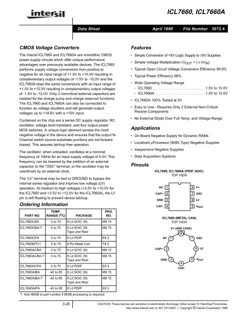
Pinouts<br />
<strong>ICL7660</strong>, <strong>ICL7660</strong>A (PDIP, SOIC)<br />
TOP VIEW<br />
NC<br />
CAP+<br />
GND<br />
CAP-<br />
CAP+<br />
<strong>ICL7660</strong> (METAL CAN)<br />
TOP VIEW<br />
NC<br />
1<br />
2<br />
3<br />
4<br />
2<br />
V+ (AND CASE)<br />
1<br />
8<br />
8<br />
7<br />
6<br />
5<br />
7<br />
V+<br />
OSC<br />
LV<br />
V OUT<br />
6<br />
OSC<br />
LV<br />
<strong>ICL7660</strong>ACBA-T 0 to 70 8 Ld SOIC (N)<br />
Tape and Reel<br />
M8.15<br />
<strong>ICL7660</strong>ACPA 0 to 70 8 Ld PDIP E8.3<br />
<strong>ICL7660</strong>AIBA -40 to 85 8 Ld SOIC (N) M8.15<br />
GND<br />
3<br />
4<br />
CAP-<br />
5<br />
V OUT<br />
<strong>ICL7660</strong>AIBA-T -40 to 85 8 Ld SOIC (N)<br />
Tape and Reel<br />
M8.15<br />
<strong>ICL7660</strong>AIPA -40 to 85 8 Ld PDIP E8.3<br />
† Add /883B to part number if 883B processing is required.<br />
3-26<br />
CAUTION: These devices are sensitive to electrostatic discharge; follow proper IC Handling Procedures.<br />
http://www.intersil.com or 407-727-9207 | Copyright © Intersil Corporation 1999
<strong>ICL7660</strong>, <strong>ICL7660</strong>A<br />
C<br />
Absolute Maximum Ratings<br />
Supply Voltage<br />
<strong>ICL7660</strong> . . . . . . . . . . . . . . . . . . . . . . . . . . . . . . . . . . . . . . . +10.5V<br />
<strong>ICL7660</strong>A . . . . . . . . . . . . . . . . . . . . . . . . . . . . . . . . . . . . . . +13.0V<br />
LV and OSC Input Voltage . . . . . . -0.3V to (V+ +0.3V) for V+ < 5.5V<br />
(Note 2) . . . . . . . . . . . . . . (V+ -5.5V) to (V+ +0.3V) for V+ > 5.5V<br />
Current into LV (Note 2) . . . . . . . . . . . . . . . . . . . 20µA for V+ > 3.5V<br />
Output Short Duration (V SUPPLY ≤ 5.5V) . . . . . . . . . . . .Continuous<br />
Thermal Information<br />
Thermal Resistance (Typical, Note 1) θ JA ( o C/W) θ JC ( o C/W)<br />
PDIP Package . . . . . . . . . . . . . . . . . . . 150 N/A<br />
SOIC Package . . . . . . . . . . . . . . . . . . . 165 N/A<br />
Metal Can Package (<strong>ICL7660</strong> Only). . . 160 70<br />
Maximum Storage Temperature Range . . . . . . . . . . -65 o C to 150 o C<br />
Maximum Lead Temperature (Soldering, 10s). . . . . . . . . . . . .300 o C<br />
(SOIC - Lead Tips Only)<br />
Operating Conditions<br />
Temperature Range<br />
<strong>ICL7660</strong>M. . . . . . . . . . . . . . . . . . . . . . . . . . . . . . . -55 o C to 125 o C<br />
<strong>ICL7660</strong>C, <strong>ICL7660</strong>AC. . . . . . . . . . . . . . . . . . . . . . . . 0 o C to 70 o C<br />
<strong>ICL7660</strong>AI . . . . . . . . . . . . . . . . . . . . . . . . . . . . . . . -40 o C to 85 o C<br />
CAUTION: Stresses above those listed in “Absolute Maximum Ratings” may cause permanent damage to the device. This is a stress only rating and operation ofthe<br />
device at these or any other conditions above those indicated in the operational sections of this specification is not implied.<br />
NOTE:<br />
1. θ JA is measured with the component mounted on an evaluation PC board in free air.<br />
Electrical Specifications <strong>ICL7660</strong> and <strong>ICL7660</strong>A, V+ = 5V, T A = 25 o C, C OSC = 0, Test Circuit Figure 11<br />
Unless Otherwise Specified<br />
<strong>ICL7660</strong><br />
<strong>ICL7660</strong>A<br />
PARAMETER SYMBOL TEST CONDITIONS<br />
MIN TYP MAX MIN TYP MAX<br />
UNITS<br />
Supply Current I+ R L = ∞ - 170 500 - 80 165 µA<br />
Supply Voltage Range - Lo V L + MIN ≤ T A ≤ MAX, R L = 10kΩ, LV to GND 1.5 - 3.5 1.5 - 3.5 V<br />
Supply Voltage Range - Hi V H + MIN ≤ T A ≤ MAX, R L = 10kΩ, LV to Open 3.0 - 10.0 3 - 12 V<br />
Output Source Resistance R OUT I OUT = 20mA, T A = 25 o C - 55 100 - 60 100 Ω<br />
I OUT = 20mA, 0 o C ≤ T A ≤ 70 o C - - 120 - - 120 Ω<br />
I OUT = 20mA, -55 o C ≤ T A ≤ 125 o C - - 150 - - - Ω<br />
I OUT = 20mA, -40 o C ≤ T A ≤ 85 o C - - - - - 120 Ω<br />
V + = 2V, I OUT = 3mA, LV to GND<br />
0 o C ≤ T A ≤ 70 o C<br />
V+ = 2V, I OUT = 3mA, LV to GND,<br />
-55 o C ≤ T A ≤ 125 o C<br />
- - 300 - - 300 Ω<br />
- - 400 - - - Ω<br />
Oscillator Frequency f OSC - 10 - - 10 - kHz<br />
Power Efficiency P EF R L = 5kΩ 95 98 - 96 98 - %<br />
Voltage Conversion Efficiency V OUT EF R L = ∞ 97 99.9 - 99 99.9 - %<br />
Oscillator Impedance Z OSC V+ = 2V - 1.0 - - 1 - MΩ<br />
V = 5V - 100 - - - - kΩ<br />
<strong>ICL7660</strong>A, V+ = 3V, T A = 25 o C, OSC = Free running, Test Circuit Figure 11, Unless Otherwise Specified<br />
Supply Current (Note 3) I+ V+ = 3V, R L = ∞, 25 o C - - - - 26 100 µA<br />
0 o C < T A
<strong>ICL7660</strong>, <strong>ICL7660</strong>A<br />
Electrical Specifications <strong>ICL7660</strong> and <strong>ICL7660</strong>A, V+ = 5V, T A = 25 o C, C OSC = 0, Test Circuit Figure 11<br />
Unless Otherwise Specified (Continued)<br />
PARAMETER SYMBOL TEST CONDITIONS<br />
<strong>ICL7660</strong><br />
<strong>ICL7660</strong>A<br />
MIN TYP MAX MIN TYP MAX<br />
Voltage Conversion Efficiency V OUT EFF V+ = 3V, R L = ∞ - - - 99 - - %<br />
T MIN < T A < T MAX - - - 99 - - %<br />
Power Efficiency P EFF V+ = 3V, R L = 5kΩ - - - 96 - - %<br />
T MIN < T A < T MAX - - - 95 - - %<br />
NOTES:<br />
2. Connecting any input terminal to voltages greater than V+ or less than GND may cause destructive latchup. It is recommended that no inputs<br />
from sources operating from external supplies be applied prior to “power up” of the <strong>ICL7660</strong>, <strong>ICL7660</strong>A.<br />
3. Derate linearly above 50 o C by 5.5mW/ o C.<br />
4. In the test circuit, there is no external capacitor applied to pin 7. However, when the device is plugged into a test socket, there is usually a very<br />
small but finite stray capacitance present, of the order of 5pF.<br />
5. The Intersil <strong>ICL7660</strong>A can operate without an external diode over the full temperature and voltage range. This device will function in existing<br />
designs which incorporate an external diode with no degradation in overall circuit performance.<br />
UNITS<br />
Functional Block Diagram<br />
V+<br />
RC<br />
OSCILLATOR ÷2<br />
VOLTAGE<br />
LEVEL<br />
TRANSLATOR<br />
CAP+<br />
CAP-<br />
V OUT<br />
OSC<br />
LV<br />
VOLTAGE<br />
REGULATOR<br />
LOGIC<br />
NETWORK<br />
Typical Performance Curves (Test Circuit of Figure 11)<br />
10<br />
10K<br />
SUPPLY VOLTAGE (V)<br />
8<br />
6<br />
4<br />
2<br />
SUPPLY VOLTAGE RANGE<br />
(NO DIODE REQUIRED)<br />
OUTPUT SOURCE RESISTANCE (Ω)<br />
1000<br />
100<br />
T A = 25 o C<br />
0<br />
-55 -25 0 25 50 100 125<br />
TEMPERATURE ( o C)<br />
FIGURE 1. OPERATING VOLTAGE AS A FUNCTION OF<br />
TEMPERATURE<br />
10<br />
0 1 2 3 4 5 6 7 8<br />
SUPPLY VOLTAGE (V+)<br />
FIGURE 2. OUTPUT SOURCE RESISTANCE AS A FUNCTION<br />
OF SUPPLY VOLTAGE<br />
3-28
<strong>ICL7660</strong>, <strong>ICL7660</strong>A<br />
Typical Performance Curves<br />
(Test Circuit of Figure 11) (Continued)<br />
OUTPUT SOURCE RESISTANCE (Ω)<br />
350<br />
300<br />
250<br />
200<br />
150<br />
100<br />
I OUT = 1mA<br />
V+ = +2V<br />
50<br />
V+ = 5V<br />
0<br />
-55 -25 0 25 50 75 100 125<br />
TEMPERATURE ( o C)<br />
POWER CONVERSION EFFICIENCY (%)<br />
100<br />
T A = 25 o C<br />
98<br />
96<br />
I OUT = 1mA<br />
94<br />
92<br />
90<br />
I OUT = 15mA<br />
88<br />
86<br />
84<br />
82<br />
V+ = +5V<br />
80<br />
100 1K 10K<br />
OSC. FREQUENCY f OSC (Hz)<br />
FIGURE 3. OUTPUT SOURCE RESISTANCE AS A FUNCTION<br />
OF TEMPERATURE<br />
FIGURE 4. POWER CONVERSION EFFICIENCY AS A<br />
FUNCTION OF OSC. FREQUENCY<br />
10K<br />
20<br />
OSCILLATOR FREQUENCY f OSC (Hz)<br />
1K<br />
100<br />
V+ = 5V<br />
T A = 25 o C<br />
10<br />
1.0 10 100 1000 10K<br />
C OSC (pF)<br />
OSCILLATOR FREQUENCY f OSC (kHz)<br />
18<br />
16<br />
14<br />
12<br />
10<br />
8<br />
V+ = +5V<br />
6<br />
-50 -25 0 25 50 75 100 125<br />
TEMPERATURE ( o C)<br />
FIGURE 5. FREQUENCY OF OSCILLATION AS A FUNCTION<br />
OF EXTERNAL OSC. CAPACITANCE<br />
FIGURE 6. UNLOADED OSCILLATOR FREQUENCY AS A<br />
FUNCTION OF TEMPERATURE<br />
OUTPUT VOLTAGE<br />
5<br />
T A = 25 o C<br />
4<br />
V+ = +5V<br />
3<br />
2<br />
1<br />
0<br />
-1<br />
-2<br />
-3<br />
-4<br />
SLOPE 55Ω<br />
-5<br />
0 10 20 30 40 50 60 70 80<br />
LOAD CURRENT I L (mA)<br />
FIGURE 7. OUTPUT VOLTAGE AS A FUNCTION OF OUTPUT<br />
CURRENT<br />
POWER CONVERSION EFFICIENCY (%)<br />
100<br />
90<br />
80<br />
70<br />
60<br />
50<br />
40<br />
30<br />
20<br />
10<br />
0<br />
100<br />
P EFF I<br />
+<br />
90<br />
80<br />
70<br />
60<br />
50<br />
40<br />
30<br />
20<br />
T A = 25 o C<br />
V + = +5V<br />
10<br />
0<br />
0 10 20 30 40 50 60<br />
LOAD CURRENT I L (mA)<br />
FIGURE 8. SUPPLY CURRENT AND POWER CONVERSION<br />
EFFICIENCY AS A FUNCTION OF LOAD<br />
CURRENT<br />
SUPPLY CURRENT I+ (mA)<br />
3-29
<strong>ICL7660</strong>, <strong>ICL7660</strong>A<br />
Typical Performance Curves<br />
(Test Circuit of Figure 11) (Continued)<br />
OUTPUT VOLTAGE<br />
+2<br />
+1<br />
0<br />
-1<br />
-2<br />
T A = 25 o C<br />
V+ = 2V<br />
SLOPE 150Ω<br />
0 1 2 3 4 5 6 7 8<br />
LOAD CURRENT I L (mA)<br />
POWER CONVERSION EFFICIENCY (%)<br />
100<br />
90<br />
80<br />
70<br />
P EFF<br />
I+<br />
20.0<br />
18.0<br />
16.0<br />
14.0<br />
60<br />
50<br />
40<br />
30<br />
20<br />
12.0<br />
10.0<br />
8.0<br />
6.0<br />
4.0<br />
10<br />
0<br />
T A =25 o C<br />
V+ = 2V<br />
2.0<br />
0<br />
0 1.5 3.0 4.5 6.0 7.5 9.0<br />
LOAD CURRENT I L (mA)<br />
SUPPLY CURRENT (mA) (NOTE 6)<br />
FIGURE 9. OUTPUT VOLTAGE AS A FUNCTION OF OUTPUT<br />
CURRENT<br />
FIGURE 10. SUPPLY CURRENT AND POWER CONVERSION<br />
EFFICIENCY AS A FUNCTION OF LOAD<br />
CURRENT<br />
NOTE:<br />
6. These curves include in the supply current that current fed directly into the load R L from the V+ (See Figure 11). Thus, approximately half the<br />
supply current goes directly to the positive side of the load, and the other half, through the <strong>ICL7660</strong>/<strong>ICL7660</strong>A, to the negative side of the load.<br />
Ideally, V OUT ∼ 2V IN , I S ∼ 2I L , so V IN x I S ∼ V OUT x I L .<br />
1<br />
8<br />
I S V+<br />
(+5V)<br />
C 1 +<br />
10µF<br />
-<br />
2<br />
3<br />
4<br />
<strong>ICL7660</strong><br />
<strong>ICL7660</strong>A<br />
7<br />
6<br />
5<br />
I L<br />
R L<br />
C OSC<br />
+<br />
(NOTE)<br />
-V OUT<br />
C 2<br />
10µF<br />
-<br />
NOTE: For large values of C OSC (>1000pF) the values of C 1 and C2 should be increased to 100µF.<br />
FIGURE 11. <strong>ICL7660</strong>, <strong>ICL7660</strong>A TEST CIRCUIT<br />
Detailed Description<br />
The <strong>ICL7660</strong> and <strong>ICL7660</strong>A contain all the necessary<br />
circuitry to complete a negative voltage converter, with the<br />
exception of 2 external capacitors which may be inexpensive<br />
10µF polarized electrolytic types. The mode of operation of<br />
the device may be best understood by considering Figure<br />
12, which shows an idealized negative voltage converter.<br />
Capacitor C 1 is charged to a voltage, V+, for the half cycle<br />
when switches S 1 and S 3 are closed. (Note: Switches S 2<br />
and S 4 are open during this half cycle.) During the second<br />
half cycle of operation, switches S 2 and S 4 are closed, with<br />
S 1 and S 3 open, thereby shifting capacitor C 1 negatively by<br />
V+ volts. Charge is then transferred from C 1 to C 2 such that<br />
the voltage on C 2 is exactly V+, assuming ideal switches and<br />
no load on C 2 . The <strong>ICL7660</strong> approaches this ideal situation<br />
more closely than existing non-mechanical circuits.<br />
In the <strong>ICL7660</strong> and <strong>ICL7660</strong>A, the 4 switches of Figure 12<br />
are MOS power switches; S 1 is a P-Channel device and S 2 ,<br />
S 3 and S 4 are N-Channel devices. The main difficulty with<br />
this approach is that in integrating the switches, the<br />
substrates of S 3 and S 4 must always remain reverse biased<br />
with respect to their sources, but not so much as to degrade<br />
their “ON” resistances. In addition, at circuit start-up, and<br />
under output short circuit conditions (V OUT = V+), the output<br />
voltage must be sensed and the substrate bias adjusted<br />
accordingly. Failure to accomplish this would result in high<br />
power losses and probable device latchup.<br />
This problem is eliminated in the <strong>ICL7660</strong> and <strong>ICL7660</strong>A by a<br />
logic network which senses the output voltage (V OUT ) together<br />
with the level translators, and switches the substrates of S 3 and<br />
S 4 to the correct level to maintain necessary reverse bias.<br />
3-30
<strong>ICL7660</strong>, <strong>ICL7660</strong>A<br />
The voltage regulator portion of the <strong>ICL7660</strong> and <strong>ICL7660</strong>A is<br />
an integral part of the anti-latchup circuitry, however its inherent<br />
voltage drop can degrade operation at low voltages. Therefore,<br />
to improve low voltage operation the “LV” pin should be<br />
connected to GROUND, disabling the regulator. For supply<br />
voltages greater than 3.5V the LV terminal must be left open to<br />
insure latchup proof operation, and prevent device damage.<br />
V IN<br />
8<br />
S 1 2 S 2<br />
C 1<br />
3<br />
S 3<br />
S 4<br />
7<br />
Theoretical Power Efficiency<br />
Considerations<br />
V OUT = -V IN<br />
FIGURE 12. IDEALIZED NEGATIVE VOLTAGE CONVERTER<br />
In theory a voltage converter can approach 100% efficiency<br />
if certain conditions are met.<br />
1. The driver circuitry consumes minimal power.<br />
2. The output switches have extremely low ON resistance<br />
and virtually no offset.<br />
3. The impedances of the pump and reservoir capacitors are<br />
negligible at the pump frequency.<br />
The <strong>ICL7660</strong> and <strong>ICL7660</strong>A approach these conditions for<br />
negative voltage conversion if large values of C 1 and C 2<br />
are used.<br />
C 2<br />
3<br />
5<br />
ENERGY IS LOST ONLY IN THE TRANSFER OF<br />
CHARGE BETWEEN CAPACITORS IF A CHANGE IN<br />
VOLTAGE OCCURS. The energy lost is defined by:<br />
E = 1 / 2 C 1 (V 1<br />
2 - V 2<br />
2 )<br />
where V 1 and V 2 are the voltages on C 1 during the pump and<br />
transfer cycles. If the impedances of C 1 and C 2 are relatively<br />
high at the pump frequency (refer to Figure 12) compared to<br />
the value of R L , there will be a substantial difference in the<br />
voltages V 1 and V 2 . Therefore it is not only desirable to make<br />
C 2 as large as possible to eliminate output voltage ripple, but<br />
also to employ a correspondingly large value for C 1 in order to<br />
achieve maximum efficiency of operation.<br />
Do’s And Don’ts<br />
1. Do not exceed maximum supply voltages.<br />
2. Do not connect LV terminal to GROUND for supply<br />
voltages greater than 3.5V.<br />
3. Do not short circuit the output to V+ supply for supply voltages<br />
above 5.5V for extended periods, however, transient<br />
conditions including start-up are okay.<br />
4. When using polarized capacitors, the + terminal of C 1<br />
must be connected to pin 2 of the <strong>ICL7660</strong> and <strong>ICL7660</strong>A<br />
and the + terminal of C 2 must be connected to GROUND.<br />
5. If the voltage supply driving the <strong>ICL7660</strong> and <strong>ICL7660</strong>A<br />
has a large source impedance (25Ω -30Ω), then a 2.2µF<br />
capacitor from pin 8 to ground may be required to limit<br />
rate of rise of input voltage to less than 2V/µs.<br />
6. User should insure that the output (pin 5) does not go<br />
more positive than GND (pin 3). Device latch up will occur<br />
under these conditions. A 1N914 or similar diode placed<br />
in parallel with C 2 will prevent the device from latching up<br />
under these conditions. (Anode pin 5, Cathode pin 3).<br />
V+<br />
+<br />
10µF<br />
-<br />
1<br />
2<br />
3<br />
4<br />
<strong>ICL7660</strong><br />
<strong>ICL7660</strong>A<br />
8<br />
7<br />
6<br />
5<br />
-<br />
V+<br />
+<br />
R O<br />
V OUT<br />
-<br />
10µF<br />
+<br />
V OUT = -V+<br />
FIGURE 13A. CONFIGURATION<br />
FIGURE 13B. THEVENIN EQUIVALENT<br />
FIGURE 13. SIMPLE NEGATIVE CONVERTER<br />
3-31
<strong>ICL7660</strong>, <strong>ICL7660</strong>A<br />
t 2 t 1<br />
B<br />
0<br />
V<br />
-(V+)<br />
A<br />
FIGURE 14. OUTPUT RIPPLE<br />
1<br />
8<br />
V+<br />
C 1<br />
2<br />
3<br />
4<br />
<strong>ICL7660</strong><br />
<strong>ICL7660</strong>A<br />
“1”<br />
7<br />
6<br />
5<br />
C 1<br />
1<br />
2<br />
3<br />
<strong>ICL7660</strong><br />
<strong>ICL7660</strong>A<br />
“n”<br />
8<br />
7<br />
6<br />
R L<br />
4<br />
5<br />
-<br />
C 2<br />
+<br />
FIGURE 15. PARALLELING DEVICES<br />
1<br />
8<br />
V+<br />
+<br />
10µF<br />
-<br />
2<br />
3<br />
4<br />
<strong>ICL7660</strong><br />
<strong>ICL7660</strong>A<br />
“1”<br />
7<br />
6<br />
5<br />
+<br />
10µF<br />
-<br />
1<br />
2<br />
3<br />
<strong>ICL7660</strong><br />
<strong>ICL7660</strong>A<br />
“n”<br />
4<br />
5<br />
-<br />
-<br />
10µF<br />
10µF +<br />
+<br />
8<br />
7<br />
6<br />
V OUT = -nV+<br />
FIGURE 16. CASCADING DEVICES FOR INCREASED OUTPUT VOLTAGE<br />
Typical Applications<br />
Simple Negative Voltage Converter<br />
The majority of applications will undoubtedly utilize the <strong>ICL7660</strong><br />
and <strong>ICL7660</strong>A for generation of negative supply voltages.<br />
Figure 13 shows typical connections to provide a negative<br />
supply negative (GND) for supply voltages below 3.5V.<br />
The output characteristics of the circuit in Figure 13A can be<br />
approximated by an ideal voltage source in series with a<br />
resistance as shown in Figure 13B. The voltage source has<br />
a value of -V+. The output impedance (R O ) is a function of<br />
the ON resistance of the internal MOS switches (shown in<br />
Figure 12), the switching frequency, the value of C 1 and C 2 ,<br />
and the ESR (equivalent series resistance) of C1 and C2. A<br />
good first order approximation for R O is:<br />
R O ≅ 2(R SW1 + R SW3 + ESR C1 ) +<br />
2(R SW2 + R SW4 + ESR C1 ) +<br />
R O ≅ 2(R SW1 + R SW3 + ESR C1 ) +<br />
1<br />
(f PUMP ) (C1)<br />
+ ESR C2<br />
f<br />
(f PUMP = OSC<br />
,R SWX = MOSFET switch resistance)<br />
2<br />
Combining the four R SWX terms as R SW , we see that:<br />
R O ≅ 2 (R SW ) +<br />
RSW, the total switch resistance, is a function of supply<br />
voltage and temperature (See the Output Source Resistance<br />
graphs), typically 23Ω at 25 o C and 5V. Careful selection of<br />
C 1 and C 2 will reduce the remaining terms, minimizing the<br />
output impedance. High value capacitors will reduce the<br />
1/(f PUMP • C 1 ) component, and low ESR capacitors will<br />
lower the ESR term. Increasing the oscillator frequency will<br />
reduce the 1/(f PUMP • C1) term, but may have the side effect<br />
of a net increase in output impedance when C 1 > 10µF and<br />
there is no longer enough time to fully charge the capacitors<br />
1<br />
(f PUMP ) (C1)<br />
+ 4 (ESR C1 ) + ESR C2<br />
3-32
<strong>ICL7660</strong>, <strong>ICL7660</strong>A<br />
every cycle. In a typical application where f OSC = 10kHz and<br />
C = C 1 = C 2 = 10µF:<br />
R O ≅ 2 (23) +<br />
R O ≅ 46 + 20 + 5 (ESR C )<br />
Since the ESRs of the capacitors are reflected in the output<br />
impedance multiplied by a factor of 5, a high value could<br />
potentially swamp out a low 1/(f PUMP • C 1 ) term, rendering an<br />
increase in switching frequency or filter capacitance ineffective.<br />
Typical electrolytic capacitors may have ESRs as high as 10Ω.<br />
R O ≅ 2 (23) +<br />
R O/ ≅ 46 + 20 + 5 (ESR C )<br />
Since the ESRs of the capacitors are reflected in the output<br />
impedance multiplied by a factor of 5, a high value could<br />
potentially swamp out a low 1/(f PUMP • C 1 ) term, rendering an<br />
increase in switching frequency or filter capacitance ineffective.<br />
Typical electrolytic capacitors may have ESRs as high as 10Ω.<br />
Output Ripple<br />
ESR also affects the ripple voltage seen at the output. The<br />
total ripple is determined by 2 voltages, A and B, as shown in<br />
Figure 14. Segment A is the voltage drop across the ESR of<br />
C 2 at the instant it goes from being charged by C 1 (current<br />
flow into C 2 ) to being discharged through the load (current<br />
flowing out of C 2 ). The magnitude of this current change is<br />
2• I OUT , hence the total drop is 2• I OUT • eSR C2 V. Segment<br />
B is the voltage change across C 2 during time t 2 , the half of<br />
the cycle when C 2 supplies current to the load. The drop at<br />
B is l OUT • t2/C 2 V. The peak-to-peak ripple voltage is the<br />
sum of these voltage drops:<br />
Again, a low ESR capacitor will reset in a higher<br />
performance output.<br />
Paralleling Devices<br />
1<br />
(5 • 10 3 ) (10 -5 )<br />
1<br />
(5 • 10 3 ) (10- 5 )<br />
+ 4 (ESR C1 ) + ESR C2<br />
+ 4 (ESR C1 ) + ESR C2<br />
V RIPPLE<br />
≅ [ 1 2 (f PUMP ) (C2) + 2 (ESR C2 )<br />
] I OUT<br />
Any number of <strong>ICL7660</strong> and <strong>ICL7660</strong>A voltage converters<br />
may be paralleled to reduce output resistance. The reservoir<br />
capacitor, C 2 , serves all devices while each device requires<br />
its own pump capacitor, C 1 . The resultant output resistance<br />
would be approximately:<br />
R OUT =<br />
R OUT (of <strong>ICL7660</strong>/<strong>ICL7660</strong>A)<br />
n (number of devices)<br />
Cascading Devices<br />
The <strong>ICL7660</strong> and <strong>ICL7660</strong>A may be cascaded as shown to<br />
produced larger negative multiplication of the initial supply<br />
voltage. However, due to the finite efficiency of each device,<br />
the practical limit is 10 devices for light loads. The output<br />
voltage is defined by:<br />
V OUT = -n (V IN ),<br />
where n is an integer representing the number of devices<br />
cascaded. The resulting output resistance would be<br />
approximately the weighted sum of the individual <strong>ICL7660</strong><br />
and <strong>ICL7660</strong>A R OUT values.<br />
Changing the <strong>ICL7660</strong>/<strong>ICL7660</strong>A Oscillator<br />
Frequency<br />
It may be desirable in some applications, due to noise or<br />
other considerations, to increase the oscillator frequency.<br />
This is achieved by overdriving the oscillator from an<br />
external clock, as shown in Figure 17. In order to prevent<br />
possible device latchup, a 1kΩ resistor must be used in<br />
series with the clock output. In a situation where the<br />
designer has generated the external clock frequency using<br />
TTL logic, the addition of a 10kΩ pullup resistor to V+ supply<br />
is required. Note that the pump frequency with external<br />
clocking, as with internal clocking, will be 1 / 2 of the clock<br />
frequency. Output transitions occur on the positive-going<br />
edge of the clock.<br />
10µF<br />
+<br />
-<br />
1<br />
2<br />
3<br />
4<br />
<strong>ICL7660</strong><br />
<strong>ICL7660</strong>A<br />
It is also possible to increase the conversion efficiency of the<br />
<strong>ICL7660</strong> and <strong>ICL7660</strong>A at low load levels by lowering the<br />
oscillator frequency. This reduces the switching losses, and is<br />
shown in Figure 18. However, lowering the oscillator<br />
frequency will cause an undesirable increase in the<br />
impedance of the pump (C 1 ) and reservoir (C 2 ) capacitors;<br />
this is overcome by increasing the values of C 1 and C 2 by the<br />
same factor that the frequency has been reduced. For<br />
example, the addition of a 100pF capacitor between pin 7<br />
(OSC) and V+ will lower the oscillator frequency to 1kHz from<br />
its nominal frequency of 10kHz (a multiple of 10), and thereby<br />
necessitate a corresponding increase in the value of C 1 and<br />
C 2 (from 10µF to 100µF).<br />
8<br />
7<br />
6<br />
5<br />
-<br />
+<br />
V+<br />
1kΩ<br />
10µF<br />
FIGURE 17. EXTERNAL CLOCKING<br />
V+<br />
V OUT<br />
CMOS<br />
GATE<br />
3-33
<strong>ICL7660</strong>, <strong>ICL7660</strong>A<br />
C 1<br />
+<br />
-<br />
Positive Voltage Doubling<br />
1<br />
2<br />
3<br />
4<br />
<strong>ICL7660</strong><br />
<strong>ICL7660</strong>A<br />
The <strong>ICL7660</strong> and <strong>ICL7660</strong>A may be employed to achieve<br />
positive voltage doubling using the circuit shown in Figure<br />
19. In this application, the pump inverter switches of the<br />
<strong>ICL7660</strong> and <strong>ICL7660</strong>A are used to charge C 1 to a voltage<br />
levelofV+-V F (where V+ is the supply voltage and V F is the<br />
forward voltage drop of diode D 1 ). On the transfer cycle, the<br />
voltage on C 1 plus the supply voltage (V+) is applied through<br />
diode D 2 to capacitor C 2 . The voltage thus created on C 2<br />
becomes (2V+) - (2VF) or twice the supply voltage minus the<br />
combined forward voltage drops of diodes D 1 and D 2 .<br />
The source impedance of the output (V OUT ) will depend on<br />
the output current, but for V+ = 5V and an output current of<br />
10mA it will be approximately 60Ω.<br />
Combined Negative Voltage Conversion<br />
and Positive Supply Doubling<br />
Figure 20 combines the functions shown in Figures 13 and<br />
Figure 19 to provide negative voltage conversion and<br />
positive voltage doubling simultaneously. This approach<br />
would be, for example, suitable for generating +9V and -5V<br />
from an existing +5V supply. In this instance capacitors C 1<br />
and C 3 perform the pump and reservoir functions<br />
respectively for the generation of the negative voltage, while<br />
capacitors C 2 and C 4 are pump and reservoir respectively<br />
for the doubled positive voltage. There is a penalty in this<br />
configuration which combines both functions, however, in<br />
that the source impedances of the generated supplies will be<br />
somewhat higher due to the finite impedance of the common<br />
charge pump driver at pin 2 of the device.<br />
8<br />
7<br />
6<br />
5<br />
-<br />
+<br />
V+<br />
C OSC<br />
C 2<br />
V OUT<br />
FIGURE 18. LOWERING OSCILLATOR FREQUENCY<br />
1<br />
2<br />
3<br />
4<br />
<strong>ICL7660</strong><br />
<strong>ICL7660</strong>A<br />
8<br />
7<br />
6<br />
5<br />
V+<br />
D 1<br />
V OUT =<br />
D 2 (2V+) - (2V F )<br />
+<br />
+<br />
C 1 - C<br />
-<br />
2<br />
FIGURE 19. POSITIVE VOLT DOUBLER<br />
C 1<br />
+<br />
-<br />
1<br />
2<br />
3<br />
4<br />
<strong>ICL7660</strong><br />
<strong>ICL7660</strong>A<br />
-<br />
C 2<br />
+<br />
Voltage Splitting<br />
The bidirectional characteristics can also be used to split a<br />
higher supply in half, as shown in Figure 21. The combined<br />
load will be evenly shared between the two sides. Because<br />
the switches share the load in parallel, the output impedance<br />
is much lower than in the standard circuits, and higher<br />
currents can be drawn from the device. By using this circuit,<br />
and then the circuit of Figure 16, +15V can be converted (via<br />
+7.5, and -7.5) to a nominal -15V, although with rather high<br />
series output resistance (~250Ω).<br />
Regulated Negative Voltage Supply<br />
8<br />
7<br />
6<br />
5<br />
In some cases, the output impedance of the <strong>ICL7660</strong> and<br />
<strong>ICL7660</strong>A can be a problem, particularly if the load current<br />
varies substantially. The circuit of Figure 22 can be used to<br />
overcome this by controlling the input voltage, via an ICL7611<br />
low-power CMOS op amp, in such a way as to maintain a<br />
nearly constant output voltage. Direct feedback is inadvisable,<br />
since the <strong>ICL7660</strong>s and <strong>ICL7660</strong>As output does not respond<br />
instantaneously to change in input, but only after the switching<br />
delay. The circuit shown supplies enough delay to<br />
accommodate the <strong>ICL7660</strong> and <strong>ICL7660</strong>A, while maintaining<br />
adequate feedback. An increase in pump and storage<br />
capacitors is desirable, and the values shown provides an<br />
output impedance of less than 5Ω to a load of 10mA.<br />
V+<br />
D 1<br />
-<br />
+<br />
C 3<br />
D 2<br />
+ - C 4<br />
V OUT =<br />
- (nV IN - V FDX )<br />
V OUT = (2V+) -<br />
(V FD1 ) - (V FD2 )<br />
FIGURE 20. COMBINED NEGATIVE VOLTAGE CONVERTER<br />
AND POSITIVE DOUBLER<br />
R L1<br />
50µF<br />
V OUT =<br />
V+ - V-<br />
2<br />
50µF<br />
R L2<br />
+<br />
-<br />
50µF<br />
+<br />
-<br />
+<br />
-<br />
1<br />
2<br />
3<br />
4<br />
<strong>ICL7660</strong><br />
<strong>ICL7660</strong>A<br />
FIGURE 21. SPLITTING A SUPPLY IN HALF<br />
8<br />
7<br />
6<br />
5<br />
V+<br />
V -<br />
3-34
<strong>ICL7660</strong>, <strong>ICL7660</strong>A<br />
Other Applications<br />
Further information on the operation and use of the <strong>ICL7660</strong><br />
and <strong>ICL7660</strong>A may be found in AN051 “Principals and<br />
Applications of the <strong>ICL7660</strong> and <strong>ICL7660</strong>A CMOS Voltage<br />
Converter”.<br />
+8V<br />
56K<br />
50K<br />
100K<br />
50K<br />
-<br />
ICL7611<br />
+<br />
+8V<br />
100Ω<br />
- 10µF<br />
+<br />
1<br />
8<br />
ICL8069<br />
100µF<br />
+<br />
-<br />
2<br />
3<br />
4<br />
<strong>ICL7660</strong><br />
<strong>ICL7660</strong>A<br />
7<br />
6<br />
5<br />
V OUT<br />
800K<br />
250K<br />
VOLTAGE<br />
ADJUST<br />
-<br />
100µF<br />
+<br />
FIGURE 22. REGULATING THE OUTPUT VOLTAGE<br />
+5V LOGIC SUPPLY<br />
12 11<br />
TTL DATA<br />
INPUT<br />
1<br />
8<br />
16<br />
4<br />
15<br />
1<br />
3<br />
RS232<br />
DATA<br />
OUTPUT<br />
+5V<br />
-5V<br />
10µF<br />
+<br />
-<br />
2<br />
3<br />
4<br />
<strong>ICL7660</strong><br />
<strong>ICL7660</strong>A<br />
7<br />
6<br />
5<br />
10µF<br />
-<br />
+<br />
IH5142<br />
13 14<br />
FIGURE 23. RS232 LEVELS FROM A SINGLE 5V SUPPLY<br />
All Intersil semiconductor products are manufactured, assembled and tested under ISO9000 quality systems certification.<br />
Intersil semiconductor products are sold by description only. Intersil Corporation reserves the right to make changes in circuit design and/or specifications at any time without<br />
notice. Accordingly, the reader is cautioned to verify that data sheets are current before placing orders. Information furnished by Intersil is believed to be accurate and<br />
reliable. However, no responsibility is assumed by Intersil or its subsidiaries for its use; nor for any infringements of patents or other rights of third parties which may result<br />
from its use. No license is granted by implication or otherwise under any patent or patent rights of Intersil or its subsidiaries.<br />
Sales Office Headquarters<br />
NORTH AMERICA<br />
Intersil Corporation<br />
P. O. Box 883, Mail Stop 53-204<br />
Melbourne, FL 32902<br />
TEL: (407) 724-7000<br />
FAX: (407) 724-7240<br />
For information regarding Intersil Corporation and its products, see web site http://www.intersil.com<br />
3-35<br />
EUROPE<br />
Intersil SA<br />
Mercure Center<br />
100, Rue de la Fusee<br />
1130 Brussels, Belgium<br />
TEL: (32) 2.724.2111<br />
FAX: (32) 2.724.22.05<br />
ASIA<br />
Intersil (Taiwan) Ltd.<br />
7F-6, No. 101 Fu Hsing North Road<br />
Taipei, Taiwan<br />
Republic of China<br />
TEL: (886) 2 2716 9310<br />
FAX: (886) 2 2715 3029