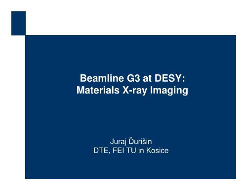
Beamline G3 at DESY: Materials X-ray Imaging
Beamline G3 at DESY: Materials X-ray Imaging
Beamline G3 at DESY: Materials X-ray Imaging

You also want an ePaper? Increase the reach of your titles
YUMPU automatically turns print PDFs into web optimized ePapers that Google loves.
<strong>Beamline</strong> <strong>G3</strong> <strong>at</strong> <strong>DESY</strong>:<br />
M<strong>at</strong>erials X-<strong>ray</strong> <strong>Imaging</strong><br />
Juraj Ďurišin<br />
DTE, FEI TU in Kosice
Why beamline <strong>G3</strong>?<br />
The majority of typical diffraction experiments determine<br />
microstructures probing larger parts of the specimen and thus<br />
averaging over the sample.<br />
But the microstructure might vary over the sample especially if it<br />
is of inhomogeneous composition or has been inhomogeneously<br />
processed (e.g. soldering, welding, brazing).
Why beamline <strong>G3</strong>?<br />
<strong>Beamline</strong> <strong>G3</strong> enables:<br />
l<strong>at</strong>eral resolution of the microstructure in direct space,<br />
visual evalu<strong>at</strong>ion of distribution of crystal phases, size of crystallites,<br />
texture or strain, structure discontinuities like surfaces, interfaces, phase<br />
or grain boundaries.<br />
crystallite<br />
1 mm<br />
Fig. 1. Crystallites of β-Sn(312)<br />
on surface of solder joint
DORIS III <strong>at</strong> <strong>DESY</strong><br />
DORIS III: storage ring for charged<br />
particles - positrons or electrons <strong>at</strong> an<br />
energy of 4.45 GeV, typically oper<strong>at</strong>es<br />
in 5 bunch mode.<br />
Beam current between 90-140 mA.<br />
Synchrotron radi<strong>at</strong>ion is produced in<br />
the bendings of the ring, where the<br />
insertion devices are loc<strong>at</strong>ed (wigglers,<br />
undul<strong>at</strong>ors, and bending magnets).<br />
The spectrum of DORIS III ranges<br />
from infrared radi<strong>at</strong>ion to hard X-<strong>ray</strong>s,<br />
and is extreme intense particularly in<br />
the X-<strong>ray</strong> range.<br />
31 beamlines.<br />
Circumference of 289 meters.<br />
It is<br />
here!<br />
Fig. 2. DORIS III<br />
[http://hasylab.desy.de]
Basic Parameters of <strong>Beamline</strong> <strong>G3</strong><br />
Monochrom<strong>at</strong>or: fixed-exit double-crystal Ge (111), also further<br />
crystals available Ge (311), Si (111), Si (511), Si (400).<br />
Wavelength range: 1 Å < λ < 2.2 Å with mirror, down to 0.5 Å<br />
without mirror (standard Ge (111) crystal).<br />
Beam dimensions <strong>at</strong> monochrom<strong>at</strong>or: ~4x16 mm 2 .<br />
Flux <strong>at</strong> the sample: ~10 8 sec -1 (depending on monochrom<strong>at</strong>or<br />
crystal and chosen energy range).
<strong>Beamline</strong> <strong>G3</strong>: Experimental St<strong>at</strong>ion<br />
Monochrom<strong>at</strong>or, slit system, air pressure shutter, scintill<strong>at</strong>ion counter,<br />
gold mirror.<br />
air pressure scintill<strong>at</strong>ion<br />
gold mirror<br />
shutter counter monochrom<strong>at</strong>or 1 st slit<br />
2 nd slit<br />
Fig. 3a. <strong>G3</strong> experimental st<strong>at</strong>ion<br />
[Rothkirch]
<strong>Beamline</strong> <strong>G3</strong>: Experimental St<strong>at</strong>ion<br />
Beam tube, gold mirror, 2 detectors, 4 circle diffractometer.<br />
detectors<br />
gold mirror<br />
4 circle<br />
diffractometer<br />
beam tube<br />
Fig. 3b. <strong>G3</strong> experimental st<strong>at</strong>ion<br />
[http://hasylab.desy.de]
<strong>Beamline</strong> <strong>G3</strong>: Monochrom<strong>at</strong>or<br />
Fixed-exit double-crystal Ge (111), also further crystals available Ge<br />
(311), Si (111), Si (511), Si (400).<br />
All movements of the monochrom<strong>at</strong>or are driven by stepper motors.<br />
The monochrom<strong>at</strong>or is w<strong>at</strong>er cooled.<br />
The tilted gold mirror (7 mrad) is used for the suppression of higher<br />
harmonics.<br />
monochrom<strong>at</strong>ic<br />
1. monocrystal beam<br />
1 st slit<br />
scintill<strong>at</strong>ion<br />
counter<br />
DORIS<br />
III<br />
polychrom<strong>at</strong>ic<br />
beam<br />
gold<br />
mirror<br />
monochrom<strong>at</strong>or<br />
box<br />
2. monocrystal<br />
(travelling)<br />
Fig. 4. <strong>G3</strong> monochrom<strong>at</strong>or<br />
2 nd slit
<strong>Beamline</strong> <strong>G3</strong>: 4 Circle Diffractometer<br />
Allows rot<strong>at</strong>ion in 4 angles: 2θ,<br />
ω, φ , χ (sample tilt: 0°< χ< 90°).<br />
Sample table enables<br />
transl<strong>at</strong>ions along x, y (±100 mm)<br />
axes and z axis (±10 mm).<br />
A sphere of 66 mm radius<br />
around the center of the<br />
diffractometer is free of<br />
mechanical components.<br />
The detector arm is equipped<br />
with a traverse allowing a radial<br />
transl<strong>at</strong>ion of the detectors of up<br />
to 380 mm.<br />
The diffractometer holds CCD<br />
detector with the MCP and<br />
point scintill<strong>at</strong>ion detector with<br />
Soller collim<strong>at</strong>or.<br />
θ/ω<br />
χ<br />
φ<br />
Ψ<br />
2θ<br />
detector arm<br />
sample table<br />
detectors<br />
Fig. 5. 4 circle diffr<strong>at</strong>ometer and detectors<br />
[http://hasylab.desy.de]
<strong>Beamline</strong> <strong>G3</strong>: Detectors<br />
Soller<br />
collim<strong>at</strong>or<br />
scintill<strong>at</strong>ion<br />
detector<br />
detector<br />
arm<br />
20.4°<br />
Fig. 5. <strong>G3</strong> detectors<br />
[http://hasylab.desy.de]<br />
microchannel<br />
pl<strong>at</strong>e<br />
CCD<br />
detector<br />
Fig. 6. Scheme of the detectors position<br />
(side view)<br />
traverse<br />
On the pl<strong>at</strong>form for the CCD/MCP detector, inclined by about 20.4º,<br />
a scintill<strong>at</strong>ion counter with Soller collim<strong>at</strong>or in front is mounted.
<strong>Beamline</strong> <strong>G3</strong>: Detectors<br />
CCD camera<br />
Hamam<strong>at</strong>su 4880,<br />
1024 x 1024 pixels (13 µm),<br />
Peltier-cooled CCD chip (-65ºC),<br />
the MCP is in contact<br />
with capton foil of the CCD camera.<br />
capton foil<br />
MCP<br />
Fig. 7. CCD camera - front view<br />
[Rothkirch]<br />
Point scintill<strong>at</strong>ion detector<br />
Ortec LABR-1X1,<br />
lanthanum bromide (LaBr 3 (Ce))<br />
detector.<br />
Fig. 8. Scintill<strong>at</strong>ion detector<br />
[www.ortec-online.com ]
<strong>Beamline</strong> <strong>G3</strong>: Microchannel pl<strong>at</strong>e<br />
The microchannel pl<strong>at</strong>e (MCP) consists of millions of very-thin, conductive<br />
glass capillaries fused together and sliced into a thin pl<strong>at</strong>e.<br />
MCP is a collim<strong>at</strong>or ar<strong>ray</strong> between the sample and a position-sensitive<br />
detector (CCD camera).<br />
Each channel of the MCP acts as a collim<strong>at</strong>or tube pointing to a certain<br />
loc<strong>at</strong>ion of the sample, channels arranged in hexagonal l<strong>at</strong>tice.<br />
Diameter of channels is 10 µm, 12.5 µm between their centers.<br />
12.5 µm<br />
Fig. 9. Microchannel pl<strong>at</strong>e<br />
(front view)<br />
[www.hamam<strong>at</strong>su.com ]<br />
Fig. 10. Scheme of the<br />
microchannel pl<strong>at</strong>e (front view)<br />
10 µm<br />
Fig. 11. Detail<br />
of hexagonal l<strong>at</strong>tice<br />
(front view)
<strong>Beamline</strong> <strong>G3</strong>: Microchannel pl<strong>at</strong>e<br />
The thickness of the pl<strong>at</strong>e is 4 mm resulting in an angular acceptance<br />
of 2.5 mrad full width and, considering the circular shape of the<br />
channels, a FWHM of 1 mrad.<br />
Typical sample to detector distance is 12 mm resulting in a sp<strong>at</strong>ial<br />
resolution of 13 µm which is also the size of each of 1024 x 1024 pixels<br />
of the CCD detector.<br />
10 µm<br />
diffracted<br />
X-<strong>ray</strong>s/<br />
fluoresence<br />
4 mm<br />
Fig. 12. Detail of hexagonal l<strong>at</strong>tice<br />
(side view)
<strong>Beamline</strong> <strong>G3</strong>: Principle of Diffraction <strong>Imaging</strong><br />
Principle of diffraction imaging lies in applic<strong>at</strong>ion of the MCP.<br />
The MCP prevents detection of crossfire<br />
from diffracted X-<strong>ray</strong>s.<br />
Sp<strong>at</strong>ial distribution of crystal phases, ...<br />
crossfire<br />
CCD<br />
camera<br />
incident<br />
beam<br />
MCP<br />
θ<br />
crossfire<br />
sample<br />
ω<br />
Fig. 13. Principle of diffraction imaging
<strong>Beamline</strong> <strong>G3</strong>: Principle of Fluorescence <strong>Imaging</strong><br />
Vari<strong>at</strong>ion of applied beam wavelength by crystal monochrom<strong>at</strong>or.<br />
The MCP prevents detection of “crossfire”<br />
from fluorescent X-<strong>ray</strong>s.<br />
Sp<strong>at</strong>ial distribution<br />
of chemical<br />
elements.<br />
crossfire<br />
CCD<br />
camera<br />
incident<br />
beam<br />
MCP<br />
Fig. 14. Effect of<br />
fluorescence<br />
crossfire<br />
sample<br />
ω<br />
Fig. 15. Principle of fluorescence imaging
<strong>Beamline</strong> <strong>G3</strong>: Parallel polycapillaries<br />
Length of 300 mm, diameter of 30 µm, arranged in a hexagonal ar<strong>ray</strong> of<br />
8 mm distance between opposing sides.<br />
Lower angular acceptance - 30 µm/ 300 mm.<br />
Small angle sc<strong>at</strong>tering - CCD does not move into the primary beam.<br />
High energy imaging - total reflection <strong>at</strong> the capillary walls is much<br />
less pronounced <strong>at</strong> high X-<strong>ray</strong> energies.<br />
parallel<br />
polycapillaries<br />
sample<br />
Fig. 16. Parallel polycapillaries <strong>at</strong> <strong>G3</strong> diffractometer<br />
[Wroblewski, Bjeoumikhov]
<strong>Beamline</strong> <strong>G3</strong>: Solid-Liquid Phase Transitions<br />
Includes applic<strong>at</strong>ion of additional monocrystal Ge (111).<br />
The monocrystal enables measurements of liquid samples.<br />
Liquid samples can not be tilted.<br />
incident<br />
beam<br />
monocrystal<br />
sample<br />
table<br />
Fig. 17. Monocrystal mounted on 4 circle<br />
diffractometer<br />
[Donges, Ovchinnikov]
<strong>Beamline</strong> <strong>G3</strong>: Solid-Liquid Phase Transitions<br />
Includes applic<strong>at</strong>ion of additional monocrystal Ge (111).<br />
Tilt angle of the monochrom<strong>at</strong>or depends on applied wavelength.<br />
end of<br />
beam<br />
tube<br />
θ 0<br />
monocrystal<br />
scintill<strong>at</strong>ion/CCD<br />
detector<br />
diffracted<br />
beam<br />
incident<br />
beam<br />
deflected<br />
beam<br />
2θ<br />
pot with<br />
liquid sample<br />
sample table<br />
(cooling/he<strong>at</strong>ing stage)<br />
Fig. 18. Principle of liquid samples measurement
<strong>Beamline</strong> <strong>G3</strong>: Solder Alloy Measurement<br />
Solder alloy: 96.5Sn3Ag0.5Cu (wt. %).<br />
The alloy was soldered on copper (Cu) foil.<br />
Goal of the measurement: visualiz<strong>at</strong>ion of distribution and<br />
orient<strong>at</strong>ion of crystal phases of the solder (β-Sn, intermetallics –<br />
Ag 3 Sn, Cu 6 Sn 5 ) via CCD camera.<br />
Samples - 2 solder spots.<br />
Ag 3 Sn<br />
β-Sn<br />
Cu 6 Sn 5<br />
Fig. 19. PCB p<strong>at</strong>tern<br />
Fig. 20. Microstructure<br />
of the solder alloy<br />
[IMR SAS]
<strong>Beamline</strong> <strong>G3</strong>: Solder Alloy Measurement<br />
1. step<br />
point scintill<strong>at</strong>ion detector,<br />
Bragg-Brentano geometry,<br />
2θ range: 30º-105º, ∆2θ=0.04º, λ = 1.54187 Å (Cu K_alpha),<br />
the solder spots positioned on the sample table of 4 circle diffractometer,<br />
Time reduction of CCD camera measurement.<br />
Intensity Intenzita [arbitrary [-]<br />
units]<br />
spot 1<br />
spot 2<br />
β-Sn<br />
Ag 3 Sn<br />
Cu 6 Sn 5<br />
Fig. 21. Diffraction p<strong>at</strong>terns of 2 solder spots
<strong>Beamline</strong> <strong>G3</strong>: Solder Alloy Measurement<br />
2. step<br />
CCD camera (detector),<br />
λ = 1.54187 Å (Cu K_alpha),<br />
2θ range selection: 2θ=60-100º, but measured was only in limit<br />
of width of Bragg peaks <strong>at</strong> their basis,<br />
∆2θ=0.04º ≈ 300 seconds.<br />
β-Sn (112)<br />
2θ = 62,52<br />
β-Sn (400)<br />
2θ = 63,64<br />
β-Sn (321)<br />
2θ = 64,44<br />
HAL spot 1000 1 HAL spot 1000 1 HAL spot 1000 1<br />
spot HAL 0 2 HAL spot 0 2 HAL spot 0 2<br />
5 mm<br />
5 mm<br />
5 mm<br />
Fig. 22. Diffraction imaging of solder spots<br />
<strong>at</strong> selected angles
<strong>Beamline</strong> <strong>G3</strong>: Solder Alloy Measurement<br />
Ag 3 Sn (032)<br />
2θ = 69,16<br />
β-Sn (420)<br />
2θ = 72,24<br />
Cu 6 Sn 5 (-733)<br />
2θ = 74,84<br />
spot 1<br />
HAL 1000<br />
spot 2<br />
HAL 0<br />
spot 1 spot 1<br />
HAL 1000<br />
HAL 1000<br />
HAL spot 0 2 HAL spot 0 2<br />
5 mm<br />
5 mm<br />
5 mm<br />
Fig. 23. Diffraction imaging of solder spots<br />
<strong>at</strong> selected angles
<strong>Beamline</strong> <strong>G3</strong>: Solder Alloy Measurement<br />
Ag 3 Sn (223)<br />
2θ = 74,80<br />
β-Sn (312)<br />
2θ = 79,48<br />
Ag 3 Sn (024)<br />
2θ = 84,98<br />
HAL 1000<br />
HAL 1000<br />
HAL spot 1000 1 spot 1 spot 1<br />
HAL 0<br />
HAL 0<br />
spot HAL 0 2 spot 2 spot 2<br />
5 mm<br />
5 mm 5 mm<br />
Fig. 24. Diffraction imaging of solder spots<br />
<strong>at</strong> selected angles
<strong>Beamline</strong> <strong>G3</strong>: Solder Alloy Measurement<br />
Brief summary<br />
<br />
<br />
Non-uniform distribution of β-Sn crystals (if crystal orient<strong>at</strong>ion<br />
taken into consider<strong>at</strong>ion),<br />
size of β-Sn crystals: ≈10 1 -10 2 µm,<br />
uniform distribution of intermetallics – Ag 3 Sn, Cu 6 Sn 5 .
Acknowledgement<br />
Thomas Wroblewski,<br />
Jörn Donges,<br />
André Rothkirch,<br />
Karel Saksl<br />
and Hermann Franz.