RF12 Universal ISM Band FSK Transceiver
RF12 Universal ISM Band FSK Transceiver
RF12 Universal ISM Band FSK Transceiver

Create successful ePaper yourself
Turn your PDF publications into a flip-book with our unique Google optimized e-Paper software.
<strong>RF12</strong> <strong>Universal</strong> <strong>ISM</strong> <strong>Band</strong><br />
<strong>FSK</strong> <strong>Transceiver</strong><br />
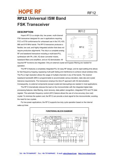
<strong>RF12</strong><br />
DESCRIPTION<br />
<strong>RF12</strong><br />
Hope’s <strong>RF12</strong> is a single chip, low power, multi-channel<br />
<strong>FSK</strong> transceiver designed for use in applications requiring<br />
FCC or ETSI conformance for unlicensed use in the 315, 433,<br />
868 and 915 MHz bands. The <strong>RF12</strong> transceiver produces a<br />
flexible, low cost, and highly integrated solution that does not<br />
require production alignments. The chip is a complete analog<br />
RF and baseband transceiver including a multi-band PLL<br />
synthesizer with PA, LNA, I/Q down converter mixers,<br />
baseband filters and amplifiers, and an I/Q demodulator. All<br />
required RF functions are integrated. Only an external crystal and bypass filtering are needed for<br />
operation.<br />
The <strong>RF12</strong> features a completely integrated PLL for easy RF design, and its rapid settling time allows<br />
for fast frequency-hopping, bypassing multi-path fading and interference to achieve robust wireless links.<br />
The PLL’s high resolution allows the usage of multiple channels in any of the bands. The receiver<br />
baseband bandwidth (BW) is programmable to accommodate various deviation, data rate and crystal<br />
tolerance requirements. The transceiver employs the Zero-IF approach with I/Q demodulation.<br />
Consequently, no external components (except crystal and decoupling) are needed in most applications.<br />
The <strong>RF12</strong> dramatically reduces the load on the microcontroller with the integrated digital data<br />
processing features: data filtering, clock recovery, data pattern recognition, integrated FIFO and TX data<br />
register. The automatic frequency control (AFC) feature allows the use of a low accuracy (low cost)<br />
crystal. To minimize the system cost, the <strong>RF12</strong> can provide a clock signal for the microcontroller, avoiding<br />
the need for two crystals.<br />
For low power applications, the <strong>RF12</strong> supports low duty cycle operation based on the internal<br />
wake-up timer.<br />
Tel: +86-755-86096587 Fax: +86-755-86096602 E-mail: sales@hoperf.com http://www.hoperf.com
FEATURES<br />
<strong>RF12</strong><br />
• Fully integrated (low BOM, easy design-in)<br />
• No alignment required in production<br />
• Fast-settling, programmable, high-resolution PLL synthesizer<br />
• Fast frequency-hopping capability<br />
• High bit rate (up to 115.2 kbps in digital mode and 256 kbps in analog mode)<br />
• Direct differential antenna input/output<br />
• Integrated power amplifier<br />
• Programmable TX frequency deviation (15 to 240 KHz)<br />
• Programmable RX baseband bandwidth (67 to 400 kHz)<br />
• Analog and digital RSSI outputs<br />
• Automatic frequency control (AFC)<br />
• Data quality detection (DQD)<br />
• Internal data filtering and clock recovery<br />
• RX synchron pattern recognition<br />
• SPI compatible serial control interface<br />
• Clock and reset signals for microcontroller<br />
• 16 bit RX Data FIFO<br />
• Two 8 bit TX data registers<br />
• Low power duty cycle mode<br />
• Standard 10 MHz crystal reference<br />
• Wake-up timer<br />
• Low power consumption<br />
• Low standby current (0.3 µA)<br />
TYPICAL APPLICATIONS<br />
• Remote control<br />
• Home security and alarm<br />
• Wireless keyboard/mouse and other PC peripherals<br />
• Toy controls<br />
• Remote keyless entry<br />
• Tire pressure monitoring<br />
• Telemetry<br />
• Personal/patient data logging<br />
• Remote automatic meter reading<br />
Tel: +86-755-86096587 Fax: +86-755-86096602 E-mail: sales@hoperf.com http://www.hoperf.com
<strong>RF12</strong><br />
DETAILED FEATURE-LEVEL DESCRIPTION<br />
The <strong>RF12</strong> <strong>FSK</strong> transceiver is designed to cover the unlicensed frequency bands at 315, 433, 868<br />
and 915 MHz. The devices facilitate compliance with FCC and ETSI requirements.<br />
The receiver block employs the Zero-IF approach with I/Q demodulation, allowing the use of a<br />
minimal number of external components in a typical application. The <strong>RF12</strong> incorporates a fully integrated<br />
multi-band PLL synthesizer, PA with antenna tuning, an LNA with switch-able gain, I/Q down converter<br />
mixers, baseband filters and amplifiers, and an I/Q demodulator followed by a data filter.<br />
PLL<br />
The programmable PLL synthesizer determines the operating frequency, while preserving accuracy<br />
based on the on-chip crystal-controlled reference oscillator. The PLL’s high resolution allows the usage of<br />
multiple channels in any of the bands.<br />
The RF VCO in the PLL performs automatic calibration, which requires only a few microseconds.<br />
Calibration always occurs when the synthesizer starts. If temperature or supply voltage changes<br />
significantly, VCO recalibration can be invoked easily. Recalibration can be initiated at any time by<br />
switching the synthesizer off and back on again.<br />
RF Power Amplifier (PA)<br />
The power amplifier has an open-collector differential output and can directly drive a loop antenna<br />
with a programmable output power level. An automatic antenna tuning circuit is built in to avoid costly<br />
trimming procedures and the so-called “hand effect.”<br />
LNA<br />
The LNA has 250 Ohm input impedance, which functions well with the proposed antennas. If the<br />
RF input of the chip is connected to 50 Ohm devices, an external matching circuit is required to provide<br />
the correct matching and to minimize the noise figure of the receiver.<br />
The LNA gain can be selected (0, –6, –14, –20 dB relative to the highest gain) according to RF signal<br />
strength. It can be useful in an environment with strong interferers.<br />
Baseband Filters<br />
The receiver bandwidth is selectable<br />
by programming the bandwidth ( BW) of<br />
the baseband filters. This allows setting<br />
up the receiver according to the<br />
characteristics of the signal to be<br />
received.<br />
An appropriate bandwidth can be<br />
chosen to accommodate various <strong>FSK</strong><br />
deviation, data rate and crystal tolerance<br />
requirements. The filter structure is 7th<br />
order Butterworth low-pass with 40 dB<br />
suppression at 2*BW frequency. Offset cancellation is done by using a high-pass filter with a cut-off<br />
frequency below 7 kHz.<br />
Tel: +86-755-86096587 Fax: +86-755-86096602 E-mail: sales@hoperf.com http://www.hoperf.com
Data Filtering and Clock Recovery<br />
<strong>RF12</strong><br />
Output data filtering can be completed by an external capacitor or by using digital filtering according<br />
to the final application.<br />
Analog operation: The filter is an RC type low-pass filter followed by a Schmitt-trigger (St). The<br />
resistor (10 kOhm) and the St are integrated on the chip. An (external) capacitor can be chosen<br />
according to the actual bit rate. In this mode, the receiver can handle up to 256 kbps data rate. The FIFO<br />
can not be used in this mode and clock is not provided for the demodulated data.<br />
Digital operation: A digital filter is used with a clock frequency at 29 times the bit rate. In this mode<br />
there is a clock recovery circuit (CR), which can provide synchronized clock to the data. Using this clock<br />
the received data can fill a FIFO. The CR has three operation modes: fast, slow, and automatic. In slow<br />
mode, its noise immunity is very high, but it has slower settling time and requires more accurate data<br />
timing than in fast mode. In automatic mode the CR automatically changes between fast and slow mode.<br />
The CR starts in fast mode, then after locking it automatically switches to slow mode (Only the digital data<br />
filter and the clock recovery use the bit rate clock. For analog operation, there is no need for setting the<br />
correct bit rate.)<br />
Data Validity Blocks<br />
RSSI<br />
A digital RSSI output is provided to monitor the input signal level. It goes high if the received signal<br />
strength exceeds a given preprogrammed level. An analog RSSI signal is also available. The RSSI<br />
settling time depends on the external filter capacitor. Pin 19 is used as analog RSSI output. The digital<br />
RSSI can be monitored by reading the status register.<br />
P1 -65 dBm 1300 mV<br />
P2 -65 dBm 1000 mV<br />
P3 -100 dBm 600 mV<br />
P4 -100 dBm 300 mV<br />
DQD<br />
The Data Quality Detector is based on counting the spikes on the unfiltered received data. For<br />
correct operation, the “DQD threshold” parameter must be filled in by using the Data Filter Command.<br />
AFC<br />
By using an integrated Automatic Frequency Control (AFC) feature, the receiver can minimize the<br />
TX/RX offset in discrete steps, allowing the use of:<br />
Tel: +86-755-86096587 Fax: +86-755-86096602 E-mail: sales@hoperf.com http://www.hoperf.com
1, Inexpensive, low accuracy crystals<br />
2, Narrower receiver bandwidth (i.e. increased sensitivity)<br />
3, Higher data rate<br />
<strong>RF12</strong><br />
Crystal Oscillator<br />
The <strong>RF12</strong> has a single-pin crystal oscillator circuit, which provides a 10 MHz reference signal for the<br />
PLL. To reduce external parts and simplify design, the crystal load capacitor is internal and<br />
programmable. Guidelines for selecting the appropriate crystal can be found later in this datasheet.<br />
The transceiver can supply the clock signal for the microcontroller; so accurate timing is possible<br />
without the need for a second crystal.<br />
When the microcontroller turns the crystal oscillator off by clearing the appropriate bit using the<br />
Configuration Setting Command, the chip provides a fixed number (196) of further clock pulses (“clock<br />
tail”) for the microcontroller to let it go to idle or sleep mode.<br />
Low Battery Voltage Detector<br />
The low battery detector circuit monitors the supply voltage and generates an interrupt if it falls below<br />
a programmable threshold level. The detector circuit has 50mV hysteresis.<br />
Wake-Up Timer<br />
The wake-up timer has very low current consumption (1.5μA typical) and can be programmed from<br />
1 ms to several days with an accuracy of ±5%.<br />
It calibrates itself to the crystal oscillator at every startup, and then at every 30 seconds. When the<br />
crystal oscillator is switched off, the calibration circuit switches it back on only long enough for a quick<br />
calibration (a few milliseconds) to facilitate accurate wake-up timing.<br />
Event Handling<br />
In order to minimize current consumption, the transceiver supports different power saving modes.<br />
Active mode can be initiated by several wake-up events (negative logical pulse on nINT input, wake-up<br />
timer timeout, low supply voltage detection, on-chip FIFO filled up or receiving a request through the<br />
serial interface).<br />
If any wake-up event occurs, the wake-up logic generates an interrupt signal, which can be used to<br />
wake up the microcontroller, effectively reducing the period the microcontroller has to be active. The<br />
source of the interrupt can be read out from the transceiver by the microcontroller through the SDO pin.<br />
Interface and Controller<br />
An SPI compatible serial interface lets the user select the frequency band, center frequency of the<br />
synthesizer, and the bandwidth of the baseband signal path. Division ratio for the microcontroller clock,<br />
wake-up timer period, and low supply voltage detector threshold are also programmable. Any of these<br />
auxiliary functions can be disabled when not needed. All parameters are set to default after power-on; the<br />
programmed values are retained during sleep mode. The interface supports the read-out of a status<br />
register, providing detailed information about the status of the transceiver and the received data.<br />
The transmitter block is equipped with an 8 bit wide TX data register. It is possible to write 8 bits into<br />
the register in burst mode and the internal bit rate generator transmits the bits out with the predefined<br />
rate.<br />
It is also possible to store the received data bits into a FIFO register and read them out in a buffered<br />
mode.<br />
Tel: +86-755-86096587 Fax: +86-755-86096602 E-mail: sales@hoperf.com http://www.hoperf.com
<strong>RF12</strong><br />
PACKAGE PIN DEFINITIONS<br />
Pin type key: D=digital, A=analog, S=supply, I=input, O=output, IO=input/output<br />
Pin Name Type Function<br />
1 SDI DI Data input of the serial control interface (SPI compatible)<br />
2 SCK DI Clock input of the serial control interface<br />
3 nSEL DI Chip select input of the serial control interface (active low)<br />
4 SDO DO Serial data output with bus hold<br />
5 nIRQ DO Interrupt request output (active low)<br />
<strong>FSK</strong> DI Transmit <strong>FSK</strong> data input<br />
6 DATA DO Received data output (FIFO not used)<br />
nFFS DI FIFO select input (active low) In FIFO mode, when bit ef is set in Configuration<br />
Setting Command<br />
DLCK DO Received data clock output (Digital filter used, FIFO not used)<br />
7 CFIL AIO External data filter capacitor connection (Analog filter used)<br />
FFIT DO<br />
FIFO interrupt (active high) Number of the bits in the RX FIFO that reach the<br />
preprogrammed limit In FIFO mode, when bit ef is set in Configuration Setting<br />
Command<br />
Tel: +86-755-86096587 Fax: +86-755-86096602 E-mail: sales@hoperf.com http://www.hoperf.com
<strong>RF12</strong><br />
8 CLK DO Microcontroller clock output<br />
Crystal connection (the other terminal of crystal to VSS) or external reference<br />
XTL AIO<br />
9<br />
input<br />
REF AIO External reference input. Use 33 pF series coupling capacitor<br />
10 nRES DIO Open drain reset output with internal pull-up and input buffer (active low)<br />
11 VSS_D S Digital VSS(Connect to VSS)<br />
12 VSS_A S Analog VSS(Connect to VSS)<br />
13 VSS_RF S RF VSS(Connect to VSS)<br />
14 RF2 AIO RF differential signal input/output<br />
15 RF1 AIO RF differential signal input/output<br />
16 VDD_RF S RF VDD(Connect to VDD)<br />
17 VDD_A S Analog VDD(Connect to VDD)<br />
18 VDD_D S Digital VDD(Connect to VDD)<br />
19 ARSSI AO Analog RSSI output<br />
20<br />
nINT DI Interrupt input (active low)<br />
VDI DO Valid data indicator output<br />
Note: The actual mode of the multipurpose pins (pin 6 and 7) is determined by the TX/RX data I/O<br />
settings of the transceiver.<br />
Typical Application<br />
Typical application with FIFO usage<br />
Tel: +86-755-86096587 Fax: +86-755-86096602 E-mail: sales@hoperf.com http://www.hoperf.com
Pin 6 Pin 7<br />
<strong>RF12</strong><br />
Transmit mode el=0 in Configuration Setting Command TX Data input -<br />
Transmit mode el=1 in Configuration Setting Command Connect to logic high -<br />
Receive mode ef=0 in Configuration Setting Command RX Data output RX Data clock output<br />
Receive mode ef=1 in Configuration Setting Command nFFS input FFIT output<br />
GENERAL DEVICE SPECIFICATION<br />
All voltages are referenced to V ss , the potential on the ground reference pin VSS.<br />
Absolute Maximum Ratings (non-operating)<br />
Symbol Parameter Min Max Units<br />
V dd Positive supply voltage -0.5 6 V<br />
V in Voltage on any pin (except RF1 and RF2) -0.5 V dd +0.5 V<br />
V oc Voltage on open collector outputs (RF1, RF2) -0.5 V dd +1.5 (Note 1) V<br />
I in Input current into any pin except VDD and VSS -25 25 mA<br />
ESD Electrostatic discharge with human body model 1000 V<br />
T st Storage temperature -55 125 oC<br />
Recommended Operating Range<br />
Symbol Parameter Min Max Units<br />
V dd Positive supply voltage 2.2 5.4 V<br />
V ocDC DC voltage on open collector outputs (RF1,RF2) V dd +1.5(Note2) V<br />
V ocAC AC peak voltage on open collector outputs (RF1,RF2) V dd -1.5(Note1) V dd +1.5 V<br />
T op Ambient operating temperature -40 85 ℃<br />
Note 1: At maximum, V dd +1.5V cannot be higher than 7V. At minimum, V dd -1.5V cannot be lower than 1.2V.<br />
Note 2: At maximum, V dd +1.5V cannot be higher than 5.5V.<br />
ELECTRICAL SPECIFICATION<br />
(Min/max values are valid over the whole recommended operating range. Typical conditions: T op = 27℃; V dd =V oc =2.7V)<br />
DC Characteristics<br />
Symbol Parameter Conditions/Notes Min Typ Max Units<br />
I dd_TX_0<br />
I dd_TX_PMAX<br />
315/433 MHz bands<br />
13 14<br />
Supply current (TX mode,<br />
868 MHz band<br />
16 18<br />
Pout = 0 dBm)<br />
915 MHz band<br />
17 19<br />
mA<br />
315/433 MHz bands<br />
21 22<br />
Supply current (TX mode,<br />
868 MHz band<br />
23 25<br />
Pout = Pmax)<br />
915 MHz band<br />
24 26<br />
mA<br />
Tel: +86-755-86096587 Fax: +86-755-86096602 E-mail: sales@hoperf.com http://www.hoperf.com
I dd_RX<br />
I pd<br />
I lb<br />
I wt<br />
I x<br />
V lb<br />
V lba<br />
V il<br />
V ih<br />
<strong>RF12</strong><br />
Supply current (RX mode)<br />
315/433 MHz bands<br />
868 MHz band<br />
915 MHz band<br />
11<br />
12<br />
13<br />
13<br />
14<br />
15<br />
mA<br />
Standby current (Sleep<br />
mode)<br />
All blocks disabled 0.3 µA<br />
Low battery voltage<br />
detector current<br />
0.5 µA<br />
consumption<br />
Wake-up timer current<br />
consumption<br />
1.5 µA<br />
Idle current<br />
Low battery detect<br />
threshold<br />
Low battery detection<br />
Crystal oscillator and<br />
3 3.5 mA<br />
baseband parts are on<br />
Programmable in 0.1 V<br />
2.2 5.3 V<br />
steps<br />
accuracy ±75<br />
Digital input low level<br />
voltage<br />
Digital input high level<br />
0.7*V dd<br />
voltage<br />
mV<br />
0.3*V dd V<br />
V<br />
I il Digital input current V il = 0 V -1 1 µA<br />
I ih Digital input current V ih = V dd , V dd = 5.4 V -1 1 µA<br />
V ol Digital output low level I ol = 2 mA 0.4 V<br />
V oh Digital output high level I oh = -2 mA V dd -0.4 V<br />
AC Characteristics (PLL parameters)<br />
Symbol Parameter Conditions/Notes Min Typ Max Units<br />
f ref<br />
PLL reference<br />
frequency<br />
(Note 1) 8 10 12 MHz<br />
Receiver LO /<br />
f o Transmitter carrier<br />
frequency<br />
315MHz band,2.5kHz resolution<br />
433MHz band,2.5kHz resolution<br />
868MHz band,5.0kHz resolution<br />
915MHz band,7.5kHz resolution<br />
310.24<br />
430.24<br />
860.48<br />
900.72<br />
319.75<br />
439.75<br />
879.51<br />
929.27<br />
Frequency error < 1kHz after<br />
t lock PLL lock time<br />
20 us<br />
10MHz step<br />
t st, P PLL startup time With a running crystal oscillator 250 us<br />
MHz<br />
Tel: +86-755-86096587 Fax: +86-755-86096602 E-mail: sales@hoperf.com http://www.hoperf.com
AC Characteristics (Receiver)<br />
<strong>RF12</strong><br />
Symbol Parameter Conditions/Notes Min Typ Max Units<br />
BW<br />
Receiver<br />
bandwidth<br />
mode 0<br />
mode 1<br />
mode 2<br />
mode 3<br />
mode 4<br />
mode 5<br />
BR <strong>FSK</strong> bit rate With internal digital filters 0.6 115.2 kbps<br />
BRA <strong>FSK</strong> bit rate With analog filter 256 kbps<br />
Receiver<br />
BER 10 -3 , BW=67kHz, BR=1.2kbps<br />
-109 -100<br />
P min<br />
dBm<br />
Sensitivity<br />
(Note 2)<br />
AFC locking range df <strong>FSK</strong> : <strong>FSK</strong> deviation in the received<br />
0.8*df <strong>FSK</strong><br />
AFC range<br />
signal<br />
Input IP3 In band interferers in high bands(868, -21<br />
IIP3 inh dBm<br />
915 MHz)<br />
IIP3 outh<br />
Input IP3 Out of band interferers l f-f o l > 4 MHz -18 dBm<br />
IIP3 inl<br />
IIP3 (LNA –6 dB In band interferers in low bands (315, -15<br />
gain)<br />
433 MHz)<br />
dBm<br />
IIP3 outl<br />
IIP3 (LNA –6 dB Out of band interferers l f-f o l > 4 MHz -12<br />
gain)<br />
dBm<br />
P max<br />
Maximum input LNA: high gain 0<br />
power<br />
dBm<br />
C in<br />
RF input<br />
1<br />
capacitance<br />
pF<br />
RS a RSSI accuracy +/-5 dB<br />
RS r RSSI range 46 dB<br />
C ARSSI<br />
Filter capacitor for<br />
1<br />
ARSSI<br />
nF<br />
RS step<br />
RSSI<br />
programmable<br />
6<br />
dB<br />
level steps<br />
DRSSI response Until the RSSI signal goes high after 500<br />
RS resp time<br />
the input signal exceeds the<br />
preprogrammed limit C ARRSI = 5 nF<br />
us<br />
AC Characteristics (Transmitter)<br />
Symbol Parameter Conditions/Notes Min Typ Max Units<br />
Open collector output DC<br />
I OUT<br />
Programmable 0.5 6 mA<br />
current<br />
P max<br />
P out<br />
P sp<br />
Available output power with<br />
optimal antenna impedance<br />
(Note 3, 4)<br />
Typical output power<br />
Spurious emission<br />
In low bands<br />
In high bands<br />
Selectable in 3 dB steps<br />
(Note 5)<br />
At max power with loop<br />
antenna (Note 6)<br />
60<br />
120<br />
180<br />
240<br />
300<br />
360<br />
P max -21<br />
67<br />
134<br />
200<br />
270<br />
350<br />
400<br />
8<br />
4<br />
75<br />
150<br />
225<br />
300<br />
375<br />
450<br />
P max<br />
dBm<br />
dBm<br />
-50 dBc<br />
kHz<br />
Tel: +86-755-86096587 Fax: +86-755-86096602 E-mail: sales@hoperf.com http://www.hoperf.com
C o<br />
Q o<br />
L out<br />
<strong>RF12</strong><br />
Output capacitance (set by the<br />
automatic antenna tuning<br />
circuit)<br />
In low bands<br />
In high bands<br />
2<br />
2.1<br />
2.6<br />
2.7<br />
3.2<br />
3.3 pF<br />
Quality factor of the output In low bands<br />
13 15 17<br />
capacitance<br />
In high bands<br />
8 10 12<br />
Output phase noise<br />
100 kHz from carrier 1<br />
-75<br />
MHz from carrier<br />
-85<br />
dBc/Hz<br />
BR <strong>FSK</strong> bit rate 256 kbps<br />
df fsk<br />
Programmable in 15 kHz<br />
<strong>FSK</strong> frequency deviation<br />
15 240 kHz<br />
steps<br />
AC Characteristics (Turn-on/Turnaround timings)<br />
Symbol Parameter Conditions/Notes Min Typ Max Units<br />
Crystal oscillator<br />
t sx<br />
Crystal ESR < 100 5 ms<br />
startup time<br />
Transmitter -<br />
T tx_rx_XTAL_ON Receiver turnover<br />
time<br />
Receiver<br />
T rx_tx_XTAL_ON -Transmitter<br />
turnover time<br />
Transmitter -<br />
T tx_rx_SYNT_ON Receiver turnover<br />
time<br />
T rx_tx_SYNT_ON<br />
Receiver<br />
-Transmitter<br />
turnover time<br />
Synthesizer off, crystal oscillator on<br />
during TX/RX change with 10 MHz<br />
step<br />
Synthesizer off, crystal oscillator on<br />
during RX/TX change with 10 MHz<br />
step<br />
Synthesizer and crystal oscillator on<br />
during TX/RX change with 10 MHz<br />
step<br />
Synthesizer and crystal oscillator on<br />
during RX/TX change with 10 MHz<br />
step<br />
450 us<br />
350 us<br />
425 us<br />
300 us<br />
AC Characteristics (Others)<br />
Symbol Parameter Conditions/Notes Min Typ Max Units<br />
C xl<br />
t POR<br />
Crystal load capacitance, see Programmable in 0.5 pF steps,<br />
8.5 16 pF<br />
crystal selection guide<br />
tolerance +/- 10%<br />
After V dd has reached 90% of<br />
Internal POR timeout<br />
100 ms<br />
final value (Note 7)<br />
t PBt Wake-up timer clock period Calibrated every 30 seconds 0.95 1.05 ms<br />
C in, D Digital input capacitance 2 pF<br />
t r , f Digital output rise/fall time 15 pF pure capacitive load 10 ns<br />
Note 1: Not using a 10 MHz crystal is allowed but not recommended because all crystal referred timing<br />
and frequency parameters will change accordingly.<br />
Note 2: See the BER diagrams in the measurement results section for detailed information (Not available<br />
at this time).<br />
Note 3: See matching circuit parameters and antenna design guide for information.<br />
Tel: +86-755-86096587 Fax: +86-755-86096602 E-mail: sales@hoperf.com http://www.hoperf.com
Note 4: Optimal antenna admittance/impedance:<br />
<strong>RF12</strong><br />
<strong>RF12</strong> Yantenna [S] Zantenna [Ohm] Lantenna [nH]<br />
315 MHz 1.5E-3 -j5.14E-3 52 + j179 98.00<br />
433 MHz 1.4E-3 -j7.1E-3 27 + j136 52.00<br />
868 MHz 2E-3 -j1.5E-2 8.7 + j66 12.50<br />
915 MHz 2.2E-3 -j1.55E-2 9 + j63 11.20<br />
Note 5: Adjustable in 8 steps.<br />
Note 6: With selective resonant antennas<br />
Note 7: During this period, commands are not accepted by the chip.<br />
CONTROL INTERFACE<br />
Commands to the transmitter are sent serially. Data bits on pin SDI are shifted into the device upon<br />
the rising edge of the clock on pin SCK whenever the chip select pin nSEL is low. When the nSEL signal<br />
is high, it initializes the serial interface. All commands consist of a command code, followed by a varying<br />
number of parameter or data bits. All data are sent MSB first (e.g. bit 15 for a 16-bit command). Bits<br />
having no influence (don’t care) are indicated with X. The Power On Reset (POR) circuit sets default<br />
values in all control and command registers.<br />
The receiver will generate an interrupt request (IT) for the microcontroller - by pulling the<br />
nIRQ pin low - on the following events:<br />
· The TX register is ready to receive the next byte (RGIT)<br />
· The FIFO has received the preprogrammed amount of bits (FFIT)<br />
· Power-on reset (POR)<br />
· FIFO overflow (FFOV) / TX register under run (RGUR)<br />
· Wake-up timer timeout (WKUP)<br />
· Negative pulse on the interrupt input pin nINT (EXT)<br />
· Supply voltage below the preprogrammed value is detected (LBD)<br />
FFIT and FFOV are applicable when the FIFO is enabled. RGIT and RGUR are applicable only when the<br />
TX register is enabled. To identify the source of the IT, the status bits should be read out.<br />
Timing Specification<br />
Symbol Parameter<br />
Minimum Value [ns]<br />
t CH Clock high time 25<br />
t CL Clock low time 25<br />
t SS Select setup time (nSEL falling edge to SCK rising edge) 10<br />
t SH Select hold time (SCK falling edge to nSEL rising edge) 10<br />
t SHI Select high time 25<br />
t DS Data setup time (SDI transition to SCK rising edge) 5<br />
t DH Data hold time (SCK rising edge to SDI transition) 5<br />
t OD Data delay time 10<br />
Tel: +86-755-86096587 Fax: +86-755-86096602 E-mail: sales@hoperf.com http://www.hoperf.com
Timing Diagram<br />
<strong>RF12</strong><br />
Control Commands<br />
Control Command<br />
Related Parameters/Functions<br />
Related control<br />
bits<br />
1<br />
Configuration Setting Frequency band, crystal oscillator load<br />
el, ef, b1 to b0,<br />
Command<br />
capacitance, baseband filter bandwidth, etc. x3 to x0<br />
2<br />
Receiver/Transmitter mode change,<br />
Power Management<br />
er, ebb, et, es,<br />
synthesizer, xtal osc, PA, wake-up timer, clock<br />
Command<br />
ex, eb, ew, dc<br />
output can be enabled here<br />
3<br />
Frequency Setting<br />
Data frequency of the local oscillator/carrier<br />
Command<br />
signal<br />
f11 to f0<br />
4 Data Rate Command Bit rate cs, r6 to r0<br />
5 Receiver Control Command<br />
Function of pin 20, Valid Data Indicator,<br />
baseband bw, LNA gain, digital RSSI threshold<br />
p20, d1 to d0, i2<br />
to i0, g1 to g0,<br />
r2 to r0<br />
6 Data Filter Command Data filter type, clock recovery parameters<br />
al, ml, s1 to s0,<br />
f2 to f0<br />
7<br />
FIFO and Reset Mode Data FIFO IT level, FIFO start control, FIFO f3 to f0, s1 to s0,<br />
Command<br />
enable and FIFO fill enable<br />
ff, fe<br />
8<br />
Receiver FIFO Read<br />
Command<br />
RX FIFO can be read with this command<br />
9 AFC Command AFC parameters<br />
a1 to a0, rl1 to<br />
rl0, st, fi, oe, en<br />
TX Configuration Control<br />
mp, m3 to m0,<br />
10 Modulation parameters, output power, ea<br />
Command<br />
p2 to p0<br />
Transmitter Register Write TX data register can be written with this<br />
11<br />
Command<br />
command<br />
t7 to t0<br />
12 Wake-Up Timer Command Wake-up time period<br />
r4 to r0, m7 to<br />
m0<br />
13 Low Duty-Cycle Command Enable low duty-cycle mode. Set duty-cycle. d6 to d0, en<br />
Tel: +86-755-86096587 Fax: +86-755-86096602 E-mail: sales@hoperf.com http://www.hoperf.com
<strong>RF12</strong><br />
Low Battery Detector and<br />
LBD voltage and microcontroller clock division d2 to d0, v4 to<br />
14 Microcontroller Clock Divider<br />
ratio<br />
v0<br />
Command<br />
15 Status Read Command Status bits can be read out<br />
In general, setting the given bit to one will activate the related function. In the following tables, the POR<br />
column shows the default values of the command registers after power-on.<br />
Description of the Control Commands<br />
1. Configuration Setting Command<br />
bit 15 14 13 12 11 10 9 8 7 6 5 4 3 2 1 0 POR<br />
1 0 0 0 0 0 0 0 el ef b1 b0 x3 x2 x1 x0 8008h<br />
Bit el enables the internal data register. If the data register is used the <strong>FSK</strong> pin must be connected to<br />
logic high level.<br />
Bit ef enables the FIFO mode. If ef=0 then DATA (pin 6) and DCLK (pin 7) are used for data and data<br />
clock output.<br />
b1 b0 Frequency <strong>Band</strong> {MHz]<br />
0 0 315<br />
0 1 433<br />
1 0 868<br />
1 1 915<br />
x3 x2 x1 x0 Crystal Load Capacitance [pF]<br />
0 0 0 0 8.5<br />
0 0 0 1 9.0<br />
0 0 1 0 9.5<br />
0 0 1 1 10.0<br />
…<br />
1 1 1 0 15.5<br />
1 1 1 1 16.0<br />
2. Power Management Command<br />
bit 15 14 13 12 11 10 9 8 7 6 5 4 3 2 1 0 POR<br />
1 0 0 0 0 0 1 0 er ebb et es ex eb ew dc 8208h<br />
Bit Function of the control bit Related blocks<br />
er<br />
Enables the whole receiver chain<br />
RF front end, baseband,<br />
synthesizer, oscillator<br />
ebb The receiver baseband circuit can be separately switched on Baseband<br />
et<br />
Switches on the PLL, the power amplifier, and starts the Power amplifier, synthesizer,<br />
transmission (If TX register is enabled)<br />
oscillator<br />
es Turns on the synthesizer Synthesizer<br />
ex Turns on the crystal oscillator Crystal oscillator<br />
eb Enables the low battery detector Low battery detector<br />
ew Enables the wake-up timer Wake-up timer<br />
dc Disables the clock output (pin 8) Clock output buffer<br />
The ebb, es, and ex bits are provided to optimize the TX to RX or RX to TX turnaround time.<br />
Tel: +86-755-86096587 Fax: +86-755-86096602 E-mail: sales@hoperf.com http://www.hoperf.com
Logic connections between power control bits:<br />
<strong>RF12</strong><br />
3. Frequency Setting Command<br />
bit 15 14 13 12 11 10 9 8 7 6 5 4 3 2 1 0 POR<br />
1 0 1 0 f11 f10 f9 f8 f7 f6 f5 f4 f3 f2 f1 f0 A680h<br />
The 12-bit parameter F (bits f11 to f0) should be in the range of 96 and 3903. When F value sent is out of<br />
range, the previous value is kept. The synthesizer band center frequency f 0 can be calculated as:<br />
f 0 = 10 * C1 * (C2 + F/4000) [MHz]<br />
The constants C1 and C2 are determined by the selected band as:<br />
<strong>Band</strong> [MHz] C1 C2<br />
315 1 31<br />
433 1 43<br />
868 2 43<br />
915 3 30<br />
Tel: +86-755-86096587 Fax: +86-755-86096602 E-mail: sales@hoperf.com http://www.hoperf.com
<strong>RF12</strong><br />
4. Data Rate Command<br />
bit 15 14 13 12 11 10 9 8 7 6 5 4 3 2 1 0 POR<br />
1 1 0 0 0 1 1 0 cs r6 r5 r4 r3 r2 r1 r0 C623h<br />
The actual bit rate in transmit mode and the expected bit rate of the received data stream in receive<br />
mode is determined by the 7-bit parameter R (bits r6 to r0) and bit cs.<br />
BR = 10000 / 29 / (R+1) / (1+cs*7) [kbps]<br />
In the receiver set R according to the next function:<br />
R= (10000 / 29 / (1+cs*7) / BR) – 1, where BR is the expected bit rate in kbps.<br />
Apart from setting custom values, the standard bit rates from 600 bps to 115.2 kbps can be<br />
approximated with small error. Data rate accuracy requirements:<br />
• Clock recovery in slow mode: ∆BR/BR < 1/(29*N bit )<br />
• Clock recovery in fast mode: ∆BR/BR < 3/(29*N bit )<br />
BR is the bit rate set in the receiver and ∆BR is the bit rate difference between the transmitter and<br />
the receiver. N bit is the maximal number of consecutive ones or zeros in the data stream. It is<br />
recommended for long data packets to include enough 1/0 and 0/1 transitions, and be careful to use the<br />
same division ratio in the receiver and in the transmitter.<br />
5. Receiver Control Command<br />
bit 15 14 13 12 11 10 9 8 7 6 5 4 3 2 1 0 POR<br />
1 0 0 1 0 p20 d1 d0 i2 i1 i0 g1 g0 r2 r1 r0 9080h<br />
Bit 10 (p20): pin20 function select<br />
p20 Function of pin 20<br />
0 Interrupt input<br />
1 VDI output<br />
Bits 9-8 (d1 to d0): VDI (valid data indicator) signal response time setting:<br />
d1 d0 Response<br />
0 0 Fast<br />
0 1 Medium<br />
1 0 Slow<br />
1 1 Always on<br />
Tel: +86-755-86096587 Fax: +86-755-86096602 E-mail: sales@hoperf.com http://www.hoperf.com
<strong>RF12</strong><br />
Bits 7-5 (i2 to i0): Receiver baseband bandwidth (BW) select:<br />
i2 i1 i0 BW [kHz]<br />
Bits 2-0 (r2 to r0): RSSI detector threshold:<br />
0 0 0 reserved<br />
0 0 1 400<br />
r2 r1 r0 RSSIsetth [dBm]<br />
0 1 0 340<br />
0 0 0 -103<br />
0 1 1 270<br />
0 0 1 -97<br />
1 0 0 200<br />
0 1 0 -91<br />
1 0 1 134<br />
0 1 1 -85<br />
1 1 0 67<br />
1 0 0 -79<br />
1 1 1 reserved<br />
1 0 1 -73<br />
1 1 0 -67<br />
Bits 4-3 (g1 to g0): LNA gain select:<br />
1 0 1 -61<br />
g1 g0 relative to maximum [dB]<br />
0 0 0<br />
0 1 -6<br />
1 0 -14<br />
1 1 -20<br />
The RSSI threshold depends on the LNA gain, the real RSSI threshold can be calculated:<br />
RSSI th = RSSI setth + G LNA<br />
6. Data Filter Command<br />
bit 15 14 13 12 11 10 9 8 7 6 5 4 3 2 1 0 POR<br />
1 1 0 0 0 0 1 0 al ml 1 s 1 f2 f1 f0 C22Ch<br />
Bit 7 (al) : Clock recovery (CR) auto lock control, if set.<br />
CR will start in fast mode, then after locking it will automatically switch to slow mode.<br />
Bit 6 (ml): Clock recovery lock control<br />
1: fast mode, fast attack and fast release (6 to 8 bit preamble (1010...) is recommended)<br />
0: slow mode, slow attack and slow release (12 to 16 bit preamble is recommended)<br />
Using the slow mode requires more accurate bit timing (see Data Rate Command).<br />
Bits 4 (s): Select the type of the data filter:<br />
s Filter Type<br />
0 Digital filter<br />
1 Analog RC filter<br />
Digital: This is a digital realization of an analog RC filter followed by a comparator with<br />
hysteresis. The time constant is automatically adjusted to the bit rate defined by the Data Rate<br />
Command.<br />
Note: Bit rate can not exceed 115 kpbs in this mode. Analog RC filter: The demodulator<br />
output is fed to pin 7 over a 10 kOhm resistor. The filter cut-off frequency is set by the external<br />
capacitor connected to this pin and VSS. C = 1 / (3 * R * Bit Rate), therefore the suggested<br />
value for 9600 bps is 3.3 nF<br />
Note: If analog RC filter is selected the internal clock recovery circuit and the FIFO can not<br />
be used.<br />
Tel: +86-755-86096587 Fax: +86-755-86096602 E-mail: sales@hoperf.com http://www.hoperf.com
<strong>RF12</strong><br />
Bits 2-0 (f2 to f0): DQD threshold parameter.<br />
Note: To let the DQD report "good signal quality" the threshold parameter should be less<br />
than 4 in the case when the bit-rate is close to the deviation. At higher deviation/bit-rate<br />
settings higher threshold parameter can report "good signal quality" as well.<br />
7. FIFO and Reset Mode Command<br />
bit 15 14 13 12 11 10 9 8 7 6 5 4 3 2 1 0 POR<br />
1 1 0 0 1 0 1 0 f3 f2 f1 f0 0 al ff dr CA80h<br />
Bits 7-4 (f4 to f0): FIFO IT level. The FIFO generates IT when the number of received data bits reaches<br />
this level.<br />
Bit 2 (al): Set the input of the FIFO fill start condition:<br />
al<br />
0 Synchron pattern<br />
1 Always fill<br />
Note: Synchron pattern is 2DD4h.<br />
Note: For details see the Configuration Setting Command<br />
For details see the Power Management Command<br />
Bit 1 (ff): FIFO fill will be enabled after synchron pattern reception. The FIFO fill stops when this bit is<br />
cleared.<br />
Bit 0 (dr): Disables the highly sensitive RESET mode. If this bit is cleared, a 200 mV glitch in the power<br />
supply may cause a system reset.<br />
Note: To restart the synchron pattern recognition, bit 1 should be cleared and set.<br />
8. Receiver FIFO Read Command<br />
bit 15 14 13 12 11 10 9 8 7 6 5 4 3 2 1 0 POR<br />
1 0 1 1 0 0 0 0 0 0 0 0 0 0 0 0 B000h<br />
With this command, the controller can read 8 bits from the receiver FIFO. Bit 6 (ef) must be set in<br />
Configuration Setting Command.<br />
Tel: +86-755-86096587 Fax: +86-755-86096602 E-mail: sales@hoperf.com http://www.hoperf.com
<strong>RF12</strong><br />
Note: The transceiver is in receive (RX) mode when bit er is set using the Power Management<br />
Command<br />
9. AFC Command<br />
bit 15 14 13 12 11 10 9 8 7 6 5 4 3 2 1 0 POR<br />
1 1 0 0 0 1 0 0 a1 a0 rl1 rl0 st fi oe en C4F7h<br />
Bit 7-6 (a1 to a0): Automatic operation mode selector:<br />
a1 a0<br />
0 0 Auto mode off (Strobe is controlled by microcontroller)<br />
0 1 Runs only once after each power-up<br />
1 0 Keep the foffset only during receiving (VDI=high)<br />
1 1 Keep the foffset value independently from the state of the VDI signal<br />
Bit 5-4 (rl1 to rl0): Range limit. Limits the value of the frequency offset register to the next values:<br />
rl1 rl0 Max deviation<br />
0 0 No restriction<br />
0 1 +15 f res to -16 f res<br />
1 0 +7 f res to -8 f res<br />
1 1 +3 f res to -4 f res<br />
f res:<br />
315, 433 MHz bands: 2.5 kHz<br />
868 MHz band: 5 kHz<br />
915 MHz band: 7.5 kHz<br />
Bit 3 (st): Strobe edge, when st goes to high, the actual latest calculated frequency error is stored into the<br />
offset register of the AFC block.<br />
Bit 2 (fi): Switches the circuit to high accuracy (fine) mode. In this case, the processing time is about twice<br />
longer, but the measurement uncertainty is about the half.<br />
Bit 1 (oe): Enables the frequency offset register. It allows the addition of the offset register to the<br />
frequency control word of the PLL.<br />
Bit 0 (en): Enables the calculation of the offset frequency by the AFC circuit.<br />
Tel: +86-755-86096587 Fax: +86-755-86096602 E-mail: sales@hoperf.com http://www.hoperf.com
<strong>RF12</strong><br />
Note:<br />
Lock bit is high when the AFC loop is locked, f same bit indicates when two subsequent measuring<br />
results are the same, toggle bit changes state in every measurement cycle.<br />
In automatic operation mode (no strobe signal is needed from the microcontroller to update the<br />
output offset register) the AFC circuit is automatically enabled when the VDI indicates potential incoming<br />
signal during the whole measurement cycle and the circuit measures the same result in two subsequent<br />
cycles.<br />
There are three operation modes, example from the possible application:<br />
1, (a1=0, a0=1) The circuit measures the frequency offset only once after power up. In this way<br />
extended TX-RX maximum distance can be achieved.<br />
Possible application:<br />
In the final application, when the user inserts the battery, the circuit measures and compensates for<br />
the frequency offset caused by the crystal tolerances. This method allows for the use of a cheaper quartz<br />
in the application and provides protection against tracking an interferer.<br />
2a, (a1=1, a0=0) The circuit automatically measures the frequency offset during an initial effective<br />
low data rate pattern –easier to receive (i.e.: 00110011) of the package and changes the receiving<br />
frequency accordingly. The further part of the package can be received by the corrected frequency<br />
settings.<br />
2b, (a1=1, a0=0) The transmitter must transmit the first part of the packet with a step higher<br />
deviation and later there is a possibility to reduce it.<br />
In both cases (2a and 2b), when the VDI indicates poor receiving conditions (VDI goes low), the<br />
output register is automatically cleared. Use these settings when receiving signals from different<br />
transmitters transmitting in the same nominal frequencies.<br />
3, (a1=1, a0=1) It’s the same as 2a and 2b modes, but suggested to use when a receiver operates<br />
with only one transmitter. After a complete measuring cycle, the measured value is kept independently of<br />
the state of the VDI signal.<br />
Tel: +86-755-86096587 Fax: +86-755-86096602 E-mail: sales@hoperf.com http://www.hoperf.com
<strong>RF12</strong><br />
10. TX Configuration Control Command<br />
bit 15 14 13 12 11 10 9 8 7 6 5 4 3 2 1 0 POR<br />
1 0 0 1 1 0 0 mp m3 m2 m1 m0 0 p2 p1 p0 9800h<br />
Bits 8-4 (mp, m3 to m0):<br />
<strong>FSK</strong> modulation parameters:<br />
The resulting output frequency can be calculated as:<br />
f out = f 0 + (-1) SIGN * (M + 1) * (15 kHz)<br />
where:<br />
f 0 is the channel center frequency (see the Frequency Setting Command)<br />
M is the four bit binary number <br />
SIGN = (mp) XOR (<strong>FSK</strong> input)<br />
Bits 2-0 (p2 to p0): Output power:<br />
p2 p1 p0 Relative Output Power [dB]<br />
0 0 0 0<br />
0 0 1 -3<br />
0 1 0 -6<br />
0 1 1 -9<br />
1 0 0 -12<br />
1 0 1 -15<br />
1 1 0 -18<br />
1 1 1 -21<br />
The output power given in the table is relative to the maximum available power, which depends on the<br />
actual antenna impedance.<br />
11. Transmitter Register Write Command<br />
bit 15 14 13 12 11 10 9 8 7 6 5 4 3 2 1 0 POR<br />
1 0 1 1 1 0 0 0 t7 t6 t5 t4 t3 t2 t1 t0 B8AAh<br />
With this command, the controller can write 8 bits (t7 to t0) to the transmitter data register. Bit 7 (el) must<br />
be set in Configuration Setting Command.<br />
Tel: +86-755-86096587 Fax: +86-755-86096602 E-mail: sales@hoperf.com http://www.hoperf.com
<strong>RF12</strong><br />
12. Wake-Up Timer Command<br />
bit 15 14 13 12 11 10 9 8 7 6 5 4 3 2 1 0 POR<br />
1 1 1 r4 r3 r2 r1 r0 m7 m6 m5 m4 m3 m2 m1 m0 E196h<br />
The wake-up time period can be calculated by (m7 to m0) and (r4 to r0):<br />
T wake-up = M * 2 R [ms]<br />
Note:<br />
• For continual operation the et bit should be cleared and set at the end of every cycle.<br />
• For future compatibility, use R in a range of 0 and 29.<br />
13. Low Duty-Cycle Command<br />
bit 15 14 13 12 11 10 9 8 7 6 5 4 3 2 1 0 POR<br />
1 1 0 0 1 0 0 r0 d6 d5 d4 d3 d2 d1 d0 en C80Eh<br />
With this command, Low Duty-Cycle operation can be set in order to decrease the average power<br />
consumption in receiver mode. The time cycle is determined by the Wake-Up Timer Command. The<br />
Duty-Cycle can be calculated by using (d6 to d0) and M. (M is parameter in a Wake-Up Timer<br />
Command.)<br />
Duty-Cycle= (D * 2 +1) / M *100%<br />
Bit 0 (en): Enables the Low Duty-Cycle Mode. Wake-up timer interrupt not generated in this mode.<br />
Note: In this operation mode, bit er must be cleared and bit ew must be set in the Power Management<br />
Command.<br />
14. Low Battery Detector and Microcontroller Clock Divider Command<br />
bit 15 14 13 12 11 10 9 8 7 6 5 4 3 2 1 0 POR<br />
1 1 0 0 0 0 0 0 d2 d1 d0 v4 v3 v2 v1 v0 C000h<br />
The 5 bit parameter (v4 to v0) represents the value V, which defines the threshold voltage V lb of the<br />
detector:<br />
V lb = 2.2 + V * 0.1 [V]<br />
Clock divider configuration:<br />
d2 d1 d0 Clock Output Frequency [ M Hz]<br />
0 0 0 1<br />
0 0 1 1.25<br />
0 1 0 1.66<br />
0 1 1 2<br />
Tel: +86-755-86096587 Fax: +86-755-86096602 E-mail: sales@hoperf.com http://www.hoperf.com
<strong>RF12</strong><br />
1 0 0 2.5<br />
1 0 1 3.33<br />
1 1 0 5<br />
1 1 1 10<br />
The low battery detector and the clock output can be enabled or disabled by bits eb and dc, respectively,<br />
using the Power Management Command.<br />
15. Status Read Command<br />
The read command starts with a zero, whereas all other control commands start with a one. If a read<br />
command is identified, the status bits will be clocked out on the SDO pin as follows:<br />
Status Register Read Sequence with FIFO Read Example:<br />
RGIT<br />
TX register is ready to receive the next byte (Can be cleared by Transmitter<br />
Register Write Command )<br />
FFIT<br />
The number of data bits in the RX FIFO has reached the pre-programmed limit (Can<br />
be cleared by any of the FIFO read methods)<br />
POR Power-on reset (Cleared after Status Read Command )<br />
RGUR TX register under run, register over write (Cleared after Status Read Command )<br />
FFOV RX FIFO overflow (Cleared after Status Read Command )<br />
WKUP Wake-up timer overflow (Cleared after Status Read Command )<br />
EXT<br />
Logic level on interrupt pin (pin 16) changed to low (Cleared after Status Read<br />
Command )<br />
LBD Low battery detect, the power supply voltage is below the pre-programmed limit<br />
FFEM FIFO is empty<br />
ATS Antenna tuning circuit detected strong enough RF signal<br />
RSSI The strength of the incoming signal is above the pre-programmed limit<br />
DQD Data quality detector output<br />
CRL Clock recovery locked<br />
ATGL Toggling in each AFC cycle<br />
OFFS(6) MSB of the measured frequency offset (sign of the offset value)<br />
OFFS(3)-OFFS(0)<br />
Offset value to be added to the value of the frequency control parameter (Four LSB<br />
bits)<br />
Tel: +86-755-86096587 Fax: +86-755-86096602 E-mail: sales@hoperf.com http://www.hoperf.com
TX REGISTER BUFFERED DATA TRANSMISSION<br />
<strong>RF12</strong><br />
In this operating mode (enabled by bit el, the Configuration Control Command) the TX data is clocked<br />
into one of the two 8-bit data registers. The transmitter starts to send out the data from the first register<br />
(with the given bit rate) when bit et is set with the Power Management Command. The initial value of the<br />
data registers (AAh) can be used to generate preamble. During this mode, the SDO pin can be monitored<br />
to check whether the register is ready (SDO is high) to receive the next byte from the microcontroller.<br />
TX register simplified block diagram (before transmit)<br />
TX register simplified block diagram (during transmit)<br />
Typical TX register usage<br />
Note: The content of the data registers are initialized by clearing bit et.<br />
Tel: +86-755-86096587 Fax: +86-755-86096602 E-mail: sales@hoperf.com http://www.hoperf.com
RX FIFO BUFFERED DATA READ<br />
<strong>RF12</strong><br />
In this operating mode, incoming data are clocked into a 16 bit FIFO buffer. The receiver starts to fill<br />
up the FIFO when the Valid Data Indicator (VDI) bit and the synchron pattern recognition circuit indicates<br />
potentially real incoming data. This prevents the FIFO from being filled with noise and overloading the<br />
external microcontroller.<br />
Polling Mode:<br />
The nFFS signal selects the buffer directly and its content can be clocked out through pin SDO by<br />
SCK. Set the FIFO IT level to 1. In this case, as long as FFIT indicates received bits in the FIFO, the<br />
controller may continue to take the bits away. When FFIT goes low, no more bits need to be taken. An<br />
SPI read command is also available.<br />
Interrupt Controlled Mode:<br />
The user can define the FIFO level (the number of received bits) which will generate the nFFIT when<br />
exceeded. The status bits report the changed FIFO status in this case.<br />
FIFO Read Example with FFIT Polling<br />
During FIFO access f SCK cannot be higher than f ref /4, where f ref is the crystal oscillator frequency.<br />
CRYSTAL SELECTION GUIDELINES<br />
The crystal oscillator of the <strong>RF12</strong> requires a 10 MHz parallel mode crystal. The circuit contains an<br />
integrated load capacitor in order to minimize the external component count. The internal load<br />
capacitance value is programmable from 8.5 pF to 16 pF in 0.5 pF steps. With appropriate PCB layout,<br />
the total load capacitance value can be 10 pF to 20 pF so a variety of crystal types can be used.<br />
When the total load capacitance is not more than 20 pF and a worst case 7 pF shunt capacitance (C 0 )<br />
value is expected for the crystal, the oscillator is able to start up with any crystal having less than 300<br />
ohms ESR (equivalent series loss resistance). However, lower C 0 and ESR values guarantee faster<br />
oscillator startup.<br />
The crystal frequency is used as the reference of the PLL, which generates the local oscillator<br />
frequency (f LO ). Therefore f LO is directly proportional to the crystal frequency. The accuracy requirements<br />
for production tolerance, temperature drift and aging can thus be determined from the maximum<br />
Tel: +86-755-86096587 Fax: +86-755-86096602 E-mail: sales@hoperf.com http://www.hoperf.com
<strong>RF12</strong><br />
allowable local oscillator frequency error.<br />
Whenever a low frequency error is essential for the application, it is possible to “pull” the crystal to<br />
the accurate frequency by changing the load capacitor value. The widest pulling range can be achieved if<br />
the nominal required load capacitance of the crystal is in the “midrange”, for example 16 pF. The<br />
“pull-ability” of the crystal is defined by its motional capacitance and C 0 .<br />
RX-TX ALIGNMENT PROCEDURES<br />
RX-TX frequency offset can be caused only by the differences in the actual reference frequency. To<br />
minimize these errors it is suggested to use the same crystal type and the same PCB layout for the<br />
crystal placement on the RX and TX PCBs.<br />
To verify the possible RX-TX offset it is suggested to measure the CLK output of both chips with a<br />
high level of accuracy. Do not measure the output at the XTL pin since the measurement process itself<br />
will change the reference frequency. Since the carrier frequencies are derived from the reference<br />
frequency, having identical reference frequencies and nominal frequency settings at the TX and RX side<br />
there should be no offset if the CLK signals have identical frequencies.<br />
It is possible to monitor the actual RX-TX offset using the AFC status report included in the status<br />
byte of the receiver. By reading out the status byte from the receiver the actual measured offset<br />
frequency will be reported. In order to get accurate values the AFC has to be disabled during the read by<br />
clearing the "en" bit in the AFC Control Command (bit 0).<br />
Tel: +86-755-86096587 Fax: +86-755-86096602 E-mail: sales@hoperf.com http://www.hoperf.com
REFERENCE DESIGNS<br />
<strong>RF12</strong><br />
Schematic<br />
PCB layout<br />
Top view<br />
Bottom view<br />
Tel: +86-755-86096587 Fax: +86-755-86096602 E-mail: sales@hoperf.com http://www.hoperf.com
SGS Reports<br />
<strong>RF12</strong><br />
Tel: +86-755-86096587 Fax: +86-755-86096602 E-mail: sales@hoperf.com http://www.hoperf.com
<strong>RF12</strong><br />
Tel: +86-755-86096587 Fax: +86-755-86096602 E-mail: sales@hoperf.com http://www.hoperf.com
<strong>RF12</strong> BONDING DIAGRAM<br />
<strong>RF12</strong><br />
Pad Opening: 85um square, except 76um octagon pads (AN1, AN2)<br />
Die Size: 2910 X 3315 um<br />
Tel: +86-755-86096587 Fax: +86-755-86096602 E-mail: sales@hoperf.com http://www.hoperf.com
<strong>RF12</strong><br />
HOPE MICROELECTRONICS CO.,LTD<br />
4/F, Block B3, East Industrial Area,<br />
Huaqiaocheng, Shenzhen, Guangdong,<br />
China<br />
Tel: 86-755-86096602<br />
Fax: 86-755-86096587<br />
Email: sales@hoperf.com<br />
Website: http://www.hoperf.com<br />
http://www.hoperf.cn<br />
http://hoperf.en.alibaba.com<br />
This document may contain preliminary information and is subject to<br />
change by Hope Microelectronics without notice. Hope Microelectronics<br />
assumes no responsibility or liability for any use of the information<br />
contained herein. Nothing in this document shall operate as an express<br />
or implied license or indemnity under the intellectual property rights of<br />
Hope Microelectronics or third parties. The products described in this<br />
document are not intended for use in implantation or other direct life<br />
support applications where malfunction may result in the direct physical<br />
harm or injury to persons. NO WARRANTIES OF ANY KIND,<br />
INCLUDING, BUT NOT LIMITED TO, THE IMPLIED WARRANTIES OF<br />
MECHANTABILITY OR FITNESS FOR A ARTICULAR PURPOSE, ARE<br />
OFFERED IN THIS DOCUMENT.<br />
©2006, HOPE MICROELECTRONICS CO.,LTD. All rights reserved.<br />
Tel: +86-755-86096587 Fax: +86-755-86096602 E-mail: sales@hoperf.com http://www.hoperf.com