Quad SPST JFET Analog Switches - Datasheet Catalog
Quad SPST JFET Analog Switches - Datasheet Catalog
Quad SPST JFET Analog Switches - Datasheet Catalog

You also want an ePaper? Increase the reach of your titles
YUMPU automatically turns print PDFs into web optimized ePapers that Google loves.
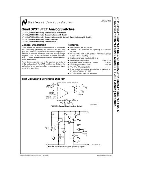
<strong>Quad</strong> <strong>SPST</strong> <strong>JFET</strong> <strong>Analog</strong> <strong>Switches</strong><br />
LF11331 LF13331 4 Normally Open <strong>Switches</strong> with Disable<br />
LF11332 LF13332 4 Normally Closed <strong>Switches</strong> with Disable<br />
LF11333 LF13333 2 Normally Closed <strong>Switches</strong> and 2 Normally Open <strong>Switches</strong> with Disable<br />
LF11201 LF13201 4 Normally Closed <strong>Switches</strong><br />
LF11202 LF13202 4 Normally Open <strong>Switches</strong><br />
General Description<br />
These devices are a monolithic combination of bipolar and<br />
<strong>JFET</strong> technology producing the industry’s first one chip<br />
quad <strong>JFET</strong> switch A unique circuit technique is employed to<br />
maintain a constant resistance over the analog voltage<br />
range of g10V The input is designed to operate from minimum<br />
TTL levels and switch operation also ensures a breakbefore-make<br />
action<br />
These devices operate from g15V supplies and swing a<br />
g10V analog signal The <strong>JFET</strong> switches are designed for<br />
applications where a dc to medium frequency analog signal<br />
needs to be controlled<br />
Test Circuit and Schematic Diagram<br />
Features<br />
FIGURE 1 Typical Circuit for One Switch<br />
January 1995<br />
Y <strong>Analog</strong> signals are not loaded<br />
Y Constant ‘‘ON’’ resistance for signals up to g10V and<br />
100 kHz<br />
Y Pin compatible with CMOS switches with the advantage<br />
of blow out free handling<br />
Y Small signal analog signals to 50 MHz<br />
Y Break-before-make action tOFF k t ON<br />
Y High open switch isolation at 10 MHz b50 dB<br />
Y Low leakage in ‘‘OFF’’ state k10 nA<br />
Y TTL DTL RTL compatibility<br />
Y Single disable pin opens all switches in package on<br />
LF11331 LF11332 LF11333<br />
Y LF11201 is pin compatible with DG201<br />
TLH5667–2<br />
LF11331LF13331LF11332LF13332LF11333LF13333LF11201<br />
LF13201LF11202LF13202 <strong>Quad</strong> <strong>SPST</strong> <strong>JFET</strong> <strong>Analog</strong> <strong>Switches</strong><br />
FIGURE 2 Schematic Diagram (Normally Open)<br />
TLH5667–12<br />
C1995 National Semiconductor Corporation<br />
TLH5667<br />
RRD-B30M75Printed in U S A
Absolute Maximum Ratings<br />
If MilitaryAerospace specified devices are required<br />
please contact the National Semiconductor Sales<br />
OfficeDistributors for availability and specifications<br />
(Note 1)<br />
Supply Voltage (V CC bV EE )<br />
Reference Voltage<br />
Logic Input Voltage<br />
<strong>Analog</strong> Voltage<br />
<strong>Analog</strong> Current<br />
36V<br />
V EE sV R sV CC<br />
V R b40VsV IN sV R a60V<br />
V EE sV A sV CC a6V<br />
V A sV EE a36V<br />
lI Al k 20 mA<br />
Power Dissipation (Note 2)<br />
Molded DIP (N Suffix)<br />
Cavity DIP (D Suffix)<br />
Operating Temperature Range<br />
LF11201 2 and LF11331 2 3<br />
LF13201 2 and LF13331 2 3<br />
Storage Temperature<br />
Soldering Information<br />
N and D Package (10 sec)<br />
SO Package<br />
Vapor Phase (60 sec)<br />
Infrared (15 sec)<br />
500 mW<br />
900 mW<br />
b55Ctoa125C<br />
0Ctoa70C<br />
b65Ctoa150C<br />
300C<br />
215C<br />
220C<br />
Electrical Characteristics (Note 3)<br />
LF1133123 LF1333123<br />
Symbol Parameter Conditions LF112012 LF132012 Units<br />
Min Typ Max Min Typ Max<br />
R ON ‘‘ON’’ Resistance V A e0 I D e1mA T A e25C 150 200 150 250 X<br />
200 300 200 350 X<br />
R ON Match ‘‘ON’’ Resistance Matching T A e25C 5 20 10 50 X<br />
V A <strong>Analog</strong> Range g10 g11 g10 g11 V<br />
I S(ON) a Leakage Current in ‘‘ON’’ Condition Switch ‘‘ON’’ V S eV D e g10V T A e25C 03 5 03 10 nA<br />
I D(ON) 3 100 3 30 nA<br />
I S(OFF) Source Current in ‘‘OFF’’ Condition Switch ‘‘OFF’’ V S ea10V T A e25C 04 5 04 10 nA<br />
V D eb10V 3 100 3 30 nA<br />
I D(OFF) Drain Current in ‘‘OFF’’ Condition Switch ‘‘OFF’’ V S ea10V<br />
01 5 01 10 nA<br />
T A e25C<br />
V D eb10V 3 100 3 30 nA<br />
V INH Logical ‘‘1’’ Input Voltage 20 20 V<br />
V INL Logical ‘‘0’’ Input Voltage 08 08 V<br />
I INH Logical ‘‘1’’ Input Current V IN e5V T A e25C 36 10 36 40 mA<br />
25 100 mA<br />
I INL Logical ‘‘0’’ Input Current V IN e08 T A e25C 01 01 mA<br />
1 1 mA<br />
t ON Delay Time ‘‘ON’’ V S e g10V (Figure 3) T A e25C 500 500 ns<br />
t OFF Delay Time ‘‘OFF’’ V S e g10V (Figure 3) T A e25C 90 90 ns<br />
t ON bt OFF Break-Before-Make V S e g10V (Figure 3) T A e25C 80 80 ns<br />
C S(OFF) Source Capacitance Switch ‘‘OFF’’ V S e g10V T A e25C 40 40 pF<br />
C D(OFF) Drain Capacitance Switch ‘‘OFF’’ V D e g10V T A e25C 30 30 pF<br />
C S(ON) a Active Source and Drain Capacitance Switch ‘‘ON’’ V S eV D e0V T A e25C 50 50 pF<br />
C D(ON)<br />
I SO(OFF) ‘‘OFF’’ Isolation (Figure 4) (Note 4) T A e25C b50 b50 dB<br />
CT Crosstalk (Figure 4) (Note 4) T A e25C b65 b65 dB<br />
SR <strong>Analog</strong> Slew Rate (Note 5) T A e25C 50 50 Vms<br />
I DIS Disable Current (Figure 5) (Note 6) T A e25C 04 10 06 15 mA<br />
06 15 09 23 mA<br />
I EE Negative Supply Current All <strong>Switches</strong> ‘‘OFF’’ V S e g10V T A e25C 30 50 43 70 mA<br />
42 75 60 105 mA<br />
I R Reference Supply Current All <strong>Switches</strong> ‘‘OFF’’ V S e g10V T A e25C 20 40 27 50 mA<br />
28 60 38 75 mA<br />
I CC Positive Supply Current All <strong>Switches</strong> ‘‘OFF’’ V S e g10V T A e25C 45 60 70 90 mA<br />
63 90 98 135 mA<br />
Note 1 Refer to RETSF11201X RETSF11331X RETSF11332X and RETSF11333X for military specifications<br />
Note 2 For operating at high temperature the molded DIP products must be derated based on a a100C maximum junction temperature and a thermal resistance<br />
of a150CW devices in the cavity DIP are based on a a150C maximum junction temperature and are derated at g100CW<br />
Note 3 Unless otherwise specified V CC ea15V V EE eb15V V R e0V and limits apply for b55CsT A sa125C for the LF1133123 and the LF112012<br />
b25CsT A sa85C for the LF1333123 and the LF132012<br />
Note 4 These parameters are limited by the pin to pin capacitance of the package<br />
Note 5 This is the analog signal slew rate above which the signal is distorted as a result of finite internal slew rates<br />
Note 6 All switches in the device are turned ‘‘OFF’’ by saturating a transistor at the disable node as shown in Figure 5 The delay time will be approximately equal<br />
to the t ON or t OFF plus the delay introduced by the external transistor<br />
Note 7 This graph indicates the analog current at which 1% of the analog current is lost when the drain is positive with respect to the source<br />
Note 8 i JA (Typical) Thermal Resistance<br />
Molded DIP (N) 85CW<br />
Cavity DIP (D) 100CW<br />
Small Outline (M) 105CW<br />
2
Connection Diagrams (Top View for SO and Dual-In-Line Packages) (All <strong>Switches</strong> Shown are For Logical ‘‘0’’)<br />
LF11331LF13331<br />
LF11332LF13332<br />
TLH5667–1<br />
TLH5667–13<br />
LF11333LF13333<br />
LF11201LF13201<br />
TLH5667–14<br />
TLH5667–15<br />
LF11202LF13202<br />
Order Number LF13201D LF11201D LF11201D883<br />
LF13202D LF11202D LF11202D883 LF13331D<br />
LF11331D LF11331D883 LF13332D LF11332D<br />
LF11332D883 LF13333D LF11333D or LH11333D883<br />
See NS Package Number D16C<br />
Order Number LF13201M LF13202M LF13331M<br />
LF13332M or LF13333M<br />
See NS Package Number M16A<br />
Order Number LF13201N LF13202N LF13331N<br />
LF13332N or LF13333N<br />
See NS Package Number N16A<br />
TLH5667–16<br />
3
Test Circuit and Typical Performance Curves<br />
Delay Time Rise Time Settling Time and Switching Transients<br />
TLH5667–3<br />
Additional Test Circuits<br />
FIGURE 3 t ON t OFF Test Circuit and Waveforms for a Normally Open Switch<br />
FIGURE 4 ‘‘OFF’’ Isolation Crosstalk Small Signal Response<br />
TLH5667–4<br />
4
Typical Performance Characteristics<br />
‘‘ON’’ Resistance ‘‘ON’’ Resistance ‘‘ON’’ Resistance Break-Before-Make Action<br />
Switching Times<br />
Crosstalk and ‘‘OFF’’<br />
Isolation vs Frequency<br />
Using Test Circuit<br />
of Figure 5 Supply Current Supply Current<br />
Supply Current Switch Leakage Currents Switch Leakage Current Switch Capacitances<br />
Slew Rate of <strong>Analog</strong><br />
Voltage Above Which<br />
Signal Loading Occurs<br />
Small Signal Response<br />
Maximum Accurate<br />
<strong>Analog</strong> Current<br />
vs Temperature<br />
Logical ‘‘1’’ Input Bias<br />
Current<br />
TLH5667–5<br />
5
Application Hints<br />
GENERAL INFORMATION<br />
These devices are monolithic quad <strong>JFET</strong> analog switches<br />
with ‘‘ON’’ resistances which are essentially independent of<br />
analog voltage or analog current The leakage currents are<br />
typically less than 1 nA at 25C in both the ‘‘OFF’’and ‘‘ON’’<br />
switch states and introduce negligible errors in most applications<br />
Each switch is controlled by minimum TTL logic<br />
levels at its input and is designed to turn ‘‘OFF’’ faster than<br />
it will turn ‘‘ON’’ This prevents two analog sources from<br />
being transiently connected together during switching The<br />
switches were designed for applications which require<br />
break-before-make action no analog current loss medium<br />
speed switching times and moderate analog currents<br />
Because these analog switches are <strong>JFET</strong> rather than<br />
CMOS they do not require special handling<br />
LOGIC INPUTS<br />
The logic input (IN) of each switch is referenced to two<br />
forward diode drops (14V at 25C) from the reference supply<br />
(V R ) which makes it compatible with DTL RTL and TTL<br />
logic families For normal operation the logic ‘‘0’’ voltage<br />
can range from 08V to b40V with respect to V R and the<br />
logic ‘‘1’’ voltage can range from 20V to 60V with respect<br />
to V R provided V IN is not greater than (V CC b25V) If the<br />
input voltage is greater than (V CC b25V) the input current<br />
will increase If the input voltage exceeds 60V or b40V<br />
with respect to V R a resistor in series with the input should<br />
be used to limit the input current to less than 100mA<br />
ANALOG VOLTAGE AND CURRENT<br />
<strong>Analog</strong> Voltage<br />
Each switch has a constant ‘‘ON’’ resistance (R ON ) for analog<br />
voltages from (V EE a5V) to (V CC b5V) For analog voltages<br />
greater than (V CC b5V) the switch will remain ON independent<br />
of the logic input voltage For analog voltages<br />
less than (V EE a5V) the ON resistance of the switch will<br />
increase Although the switch will not operate normally<br />
when the analog voltage is out of the previously mentioned<br />
range the source voltage can go to either (V EE a36V) or<br />
(V CC a6V) whichever is more positive and can go as negative<br />
as V EE without destruction The drain (D) voltage can<br />
also go to either (V EE a36V) or (V CC a6V) whichever is<br />
more positive and can go as negative as (V CC b36V) without<br />
destruction<br />
<strong>Analog</strong> Current<br />
With the source (S) positive with respect to the drain (D) the<br />
R ON is constant for low analog currents but will increase at<br />
higher currents (l5 mA) when the FET enters the saturation<br />
region However if the drain is positive with respect to<br />
the source and a small analog current loss at high analog<br />
currents (Note 6) is tolerable a low R ON can be maintained<br />
for analog currents greater than 5 mA at 25C<br />
LEAKAGE CURRENTS<br />
The drain and source leakage currents in both the ON and<br />
the OFF states of each switch are typically less than 1 nA<br />
at 25C and less than 100 nA at 125C As shown in the<br />
typical curves these leakage currents are Dependent on<br />
power supply voltages analog voltage analog current and<br />
the source to drain voltage<br />
DELAY TIMES<br />
The delay time OFF (t OFF ) is essentially independent of<br />
both the analog voltage and temperature The delay time<br />
ON (t ON ) will decrease as either (V CC bV A ) decreases or<br />
the temperature decreases<br />
POWER SUPPLIES<br />
The voltage between the positive supply (V CC ) and either<br />
the negative supply (V EE ) or the reference supply (V R ) can<br />
be as much as 36V To accommodate variations in input<br />
logic reference voltages V R can range from V EE to<br />
(V CC b45V) Care should be taken to ensure that the power<br />
supply leads for the device never become reversed in polarity<br />
or that the device is never inadvertantly installed backwards<br />
in a test socket If one of these conditions occurs the<br />
supplies would zener an internal diode to an unlimited current<br />
and result in a destroyed device<br />
SWITCHING TRANSIENTS<br />
When a switch is turned OFF or ON transients will appear<br />
at the load due to the internal transient voltage at the gate<br />
of the switch <strong>JFET</strong> being coupled to the drain and source by<br />
the junction capacitances of the <strong>JFET</strong> The magnitude of<br />
these transients is dependent on the load A lower value R L<br />
produces a lower transient voltage A negative transient occurs<br />
during the delay time ON while a positive transient<br />
occurs during the delay time OFF These transients are relatively<br />
small when compared to faster switch families<br />
DISABLE NODE<br />
This node can be used as shown in Figure 5 to turn all the<br />
switches in the unit off independent of logic inputs Normally<br />
the node floats freely at an internal diode drop (07V)<br />
above V R When the external transistor in Figure 5 is saturated<br />
the node is pulled very close to V R and the unit is<br />
disabled Typically the current from the node will be less<br />
than 1 mA This feature is not available on the LF11201 or<br />
LF11202 series<br />
FIGURE 5 Disable Function<br />
TLH5667–6<br />
6
Typical Applications<br />
Sample and Hold with Reset<br />
Programmable Inverting Non-Inverting Operational Amplifier<br />
Programmable Gain Operational Amplifier<br />
TLH5667–7<br />
7
Typical Applications (Continued)<br />
Demultiplexer<br />
MultiplexerMixer<br />
8-Channel <strong>Analog</strong> Commutator with 6-Channel Select Logic<br />
8<br />
TLH5667–8
Typical Applications (Continued)<br />
Chopper Channel Amplifier<br />
Self-Zeroing Operational Amplifier<br />
TLH5667–9<br />
9
Typical Applications (Continued)<br />
Programmable Integrator with Reset and Hold<br />
Staircase Transfer Function Operational Amplifier<br />
TLH5667–10<br />
10
Typical Applications (Continued)<br />
DSB Modulator-Demodulator<br />
TLH5667–11<br />
11
Physical Dimensions inches (millimeters)<br />
Order Number LF11201D LF11201D883 LF13201D LF11202D LF11202D883 LF13202D LF11331D<br />
LF11331D883 LF13331D LF11332D LF11332D883 LF13332D LF11333D LF11333D883 or LF13333D<br />
NS Package Number D16C<br />
Order Number LF13201M LF13202M<br />
LF13331M LF13332M or LF13333M<br />
NS Package Number M16A<br />
13
LF11331LF13331LF11332LF13332LF11333LF13333LF11201<br />
LF13201LF11202LF13202 <strong>Quad</strong> <strong>SPST</strong> <strong>JFET</strong> <strong>Analog</strong> <strong>Switches</strong><br />
Physical Dimensions inches (millimeters)<br />
Order Number LF13201N LF13202N LF13331N LF13332N or LF13333N<br />
NS Package Number N16A<br />
LIFE SUPPORT POLICY<br />
NATIONAL’S PRODUCTS ARE NOT AUTHORIZED FOR USE AS CRITICAL COMPONENTS IN LIFE SUPPORT<br />
DEVICES OR SYSTEMS WITHOUT THE EXPRESS WRITTEN APPROVAL OF THE PRESIDENT OF NATIONAL<br />
SEMICONDUCTOR CORPORATION As used herein<br />
1 Life support devices or systems are devices or 2 A critical component is any component of a life<br />
systems which (a) are intended for surgical implant support device or system whose failure to perform can<br />
into the body or (b) support or sustain life and whose be reasonably expected to cause the failure of the life<br />
failure to perform when properly used in accordance support device or system or to affect its safety or<br />
with instructions for use provided in the labeling can effectiveness<br />
be reasonably expected to result in a significant injury<br />
to the user<br />
National Semiconductor National Semiconductor National Semiconductor National Semiconductor National Semiconductores National Semiconductor<br />
Corporation GmbH Japan Ltd Hong Kong Ltd Do Brazil Ltda (Australia) Pty Ltd<br />
2900 Semiconductor Drive Livry-Gargan-Str 10 Sumitomo Chemical 13th Floor Straight Block Rue Deputado Lacorda Franco Building 16<br />
PO Box 58090 D-82256 F4urstenfeldbruck Engineering Center Ocean Centre 5 Canton Rd 120-3A Business Park Drive<br />
Santa Clara CA 95052-8090 Germany Bldg 7F Tsimshatsui Kowloon Sao Paulo-SP Monash Business Park<br />
Tel 1(800) 272-9959 Tel (81-41) 35-0 1-7-1 Nakase Mihama-Ku Hong Kong Brazil 05418-000 Nottinghill Melbourne<br />
TWX (910) 339-9240 Telex 527649 Chiba-City Tel (852) 2737-1600 Tel (55-11) 212-5066 Victoria 3168 Australia<br />
Fax (81-41) 35-1 Ciba Prefecture 261 Fax (852) 2736-9960 Telex 391-1131931 NSBR BR Tel (3) 558-9999<br />
Tel (043) 299-2300 Fax (55-11) 212-1181 Fax (3) 558-9998<br />
Fax (043) 299-2500<br />
National does not assume any responsibility for use of any circuitry described no circuit patent licenses are implied and National reserves the right at any time without notice to change said circuitry and specifications
This datasheet has been download from:<br />
www.datasheetcatalog.com<br />
<strong>Datasheet</strong>s for electronics components.