6802 - AndysArcade.De
6802 - AndysArcade.De
6802 - AndysArcade.De

You also want an ePaper? Increase the reach of your titles
YUMPU automatically turns print PDFs into web optimized ePapers that Google loves.
MC<strong>6802</strong><br />
MC6808<br />
MC<strong>6802</strong>NS<br />
MICROPROCESSOR WITH CLOCK AND OPTIONAL RAM<br />
The MC<strong>6802</strong> is a monolithic 8-bit microprocessor that contains all the<br />
registers and accumulators of the present MC~OO plus an internal clock<br />
oscillator and driver on the same chip. In addition, the MCW02 has 128<br />
bytes of on-board RAM located at hex addresses $~ to $O07F. The<br />
first 32 bytes of RAM, at hex addresses $~ to $001 F, may be retained<br />
in a low power mode by utilizing VCC standby; thus, facilitating<br />
memory ietention during a power-down situation.<br />
The MC<strong>6802</strong> is completely software compatible with the MC68W as<br />
well as the entire M~W family of parts. Hence, the MC<strong>6802</strong> is expandable<br />
to WK words.<br />
The MC<strong>6802</strong>NS is identical to the MC<strong>6802</strong> without standby RAM<br />
feature. The MC6808 is identical to the MC<strong>6802</strong> without on-board<br />
RAM,<br />
● On-Chip Clock Circuit<br />
● 128x8 Bit On-Chip RAM<br />
~>,,~<br />
● 32 Bytes of RAM are Retainable<br />
;\J:<br />
.!$;~,~:<br />
● Software-Compatible with the MC68~ ~\R,!. t<br />
*$\i,<br />
● Expandable to 64K Words<br />
‘$. ~.~., $\iM<br />
~..;,, ,<br />
.,,<br />
,W ..,~$!,‘~<br />
● Standard TTL-Compatible Inputs and Outputs<br />
..<br />
~.~:;, ‘>~.<br />
.*.:Xl~,o,,<br />
,?<br />
● 8-Bit Word Size<br />
.f+$.t,,. *$,,<br />
.1,>,, ~,.t..~.$<br />
. 16-8it Memory Addressing ~:t<br />
● Interrupt Capability<br />
,, ,.,..<br />
,,.,)?<br />
.,.<br />
,$$.!.,<br />
..\,.\.\,<br />
+$;, ,{, ~.$>&, .<br />
,,:.4,.,~.><br />
,,\\,<br />
.:s$..<br />
‘J.i:..$<br />
,..b~>l,i,y.<br />
><br />
~y$ ,’ ... ~./,,<br />
.,,.,{+? ,,“<br />
‘,{$;:,?.:$: ~s.q, ~~,i$~<br />
.,,. a:.,,3,,<br />
,~,i , ..>.,’, ~~ .:>,\\.)t. ~’<br />
,,.,,a,+:>., ‘~,.-’<br />
?;:t .~,~<br />
,.KK,*?‘...f$,+ ~J:<br />
~,,,<br />
;.!,, !::,,<br />
~.?., ,..,. .,J~<br />
~,,).$ ,,~t~r.tc ,>....,..,.<br />
ORD&Q~,~lJjFOR<br />
,,,$% ~~.*> MATION<br />
,,:, ,,.<br />
Package Type Freq&&nc$@fiz) Temperature Order Number<br />
Ceramic<br />
,,{.:.<br />
:$:f~ls$<br />
Ooc to 70”C M C<strong>6802</strong>L<br />
~:,,“v \<br />
L Suffix ~~ *?.O – 40°C to 85°C MCM02CL<br />
,““.NA.Jx$:i<br />
~:?:$>l ,. \<br />
,if .,:\<br />
1.5 O“c to 70”C M C68A02L<br />
.\:.\ a “<br />
.,.. .,.;(>~ti~ 1.5 –40°C to 85°C M C68A02CL<br />
*..l..~’!::::<br />
..%<br />
~\J., .13,,iv,<br />
1.5 O“c to 70°c MC68A08L<br />
,3* ,\<br />
t.i.v,\ 2.0 Ooc to 700c MC68B02L<br />
>;~j.’,.]. ~~\ .,<br />
,~,~~,.,t:; . 2.0 O“c to 70°c MC68B08L<br />
~e~ti~ 1.0 O“c to 700c MC<strong>6802</strong>P<br />
P Suffix 1.0 –40°C to 85°C MC<strong>6802</strong>CP<br />
1.0 Ooc to 700c M C<strong>6802</strong>N SP<br />
1.0 Ooc to 700c M C6808P<br />
1.5 Ooc to 700c MC68A02P<br />
1.5 –40°C to 85°C M C68A02CP<br />
1.5 O“c to 70°c M C68A08P<br />
2.0 Ooc to 700c MC68B02P<br />
2.0 O“c to 700c MC68B08P<br />
..,,..,, t..>i ..<br />
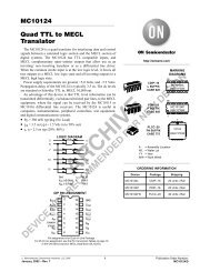
PIN<br />
ASSIGNMENT<br />
P SUFFIX<br />
LASTIC PACKAGE<br />
CASE 711<br />
Vss[ 1. 40 )fl EsET<br />
HALT[ 2 39 ]EXTAL<br />
VR[ 3 38 ] XTAL<br />
FQ [ 4 37 ]E<br />
VLIA[ 5 36 ] RE**<br />
NMI[ 6 35 ] VCC Standby*<br />
BA[ 7 34 J R/~<br />
Vcc[ 8 33 ] DO<br />
AO [ 9<br />
32 ]Dl<br />
Al [ 10 31 ]D2<br />
A2 [ 11<br />
A3 ~ 12<br />
30 ] D3<br />
29 ] D4<br />
A4 [ 13 28 ] D5<br />
A5 [ 14 27 ] D6<br />
A6 [ 15<br />
26 ] D7<br />
A7 [ 16 25 ]A15<br />
A8 [ 1? 24 ]A14<br />
A9 [ 18 23 ]A13<br />
A1O[ 19 22 ]A12<br />
* pin 35 mUSt be tied to 5 V on the MC<strong>6802</strong>NS<br />
* * pin 36 must be tied to ground for the Mc6808<br />
@MOTOROLA lNc , 1984 DS9818-R3
TYPICAL<br />
MICROCOMPUTER<br />
Vcc Vcc Vcc ,<br />
0 0<br />
Counter/<br />
M C6W6 - ~Q _<br />
This block diagram shows a typical cost effective<br />
microcomputer. The MPU is the<br />
Timer 1/0<br />
RESET +<br />
15 ROM, 1/0, Timer 1<br />
- MR<br />
RESET Cso ~ VMA VMA HALT -<br />
center of the microcomputer svstem and is<br />
~ Clock<br />
shown in a minimum system interfacing ~hh<br />
~ 2 k BVtes ROM<br />
E<br />
RE +<br />
R1~<br />
— a ROM combination chip. It is not int.~n~<br />
~ 10 !/0 Lines<br />
that this svstem be limited to this,C{~~~&*<br />
R‘ w MC<strong>6802</strong> ml -<br />
Parallel ~ 3 Lines Timer<br />
but that it be expandable with ot@r ‘~@&ln<br />
MPU BA -<br />
\ *\*:,<br />
IJO ~<br />
the M6800 Microcomputer faml$~,tts$j:{$iW<br />
DO-D7 DO-D7 DO-D7<br />
—<br />
\*.SS::[.:,j.:.<br />
EXTAL ~<br />
*T ...,.~i.,.+..<br />
~l!,:l!, ,~<br />
~<br />
\\J,<br />
~<br />
.,)... ,.:~~:: ‘><br />
o<br />
,t;+:<br />
i..,~:<br />
CP2 AO-A1O,<br />
\:,q::,$q?>:J,f<br />
Control<br />
AO-A15<br />
{n CPI<br />
Csl<br />
AO-A15 XTAL -<br />
.~.!.. t,:$<br />
~.:... ,. ,$.~<br />
i,, \,Ii\.<br />
—<br />
.>,$., ,.,,.~i. ‘&?<br />
., \,*i.,!.,,,~:,!,<br />
‘<br />
-...2:.p.,<br />
,’,> *.>\) lit.<br />
‘~.’ ,.,<br />
.f:~s,,)W<br />
~’~?l~. ‘,, $~: ‘*K>+.}! *ii,”<br />
MAXIMUM RATINGS<br />
\,, ~><br />
‘**. ,“~~~’ -<br />
Rating SVmbol Value<br />
Unit ,,$:,Th[s\,{~put contains circuitrv to protect the<br />
SupplV Voltage Vcc –0.3 to +7.0 v<br />
“!*!KQutS against<br />
:&+,,,e..!:.,.,<br />
damage due to high static<br />
Input Voltage Vin –0.3 to +7.0<br />
v ~a;$$~:~~~$t~ltagesor eleCttiC fields; however, it is ad.<br />
~t vised that normal precautions be taken to<br />
Operating Temperature Range<br />
*,:?IW~ .’ ~’:< ,:,,\>.*’<br />
avoid application of anv voltage higher than<br />
M C<strong>6802</strong>, M C680A02, M C680B02<br />
oto +70 -?~::~’ maximum rated voltages to this highimpedance<br />
circuit. Reliability of operation is<br />
.- .<br />
M C<strong>6802</strong>C, M C680A02C TA – 40 to + 8p
DC ELECTRICAL CHARACTERISTICS (Vcr = 5.0 Vdc f 5%, VSR = 0, TA = O to 70”C, unless otherwise noted)<br />
I Characteristic I Svmb 01 I Min I TVD I Max I Unit I<br />
Input High Voltage<br />
Logic, EXTAL VIH I v~~+2.0 t - I v~~ I ,, I<br />
RESET >> ~~u “ LL<br />
Input Low Voltage Logic, EXTAL, RESET .— ;s–0.3 — Vss+O.8 v<br />
Input Leakage Current (Vin =0 to 5.25 V, VCC= max)<br />
Logic Iin — 1.0 2.5 PA<br />
Output High Voltage ,+!.<br />
..8<br />
(l Load= –205pA, Vcc=min)<br />
DO-D7 VSS+2.4 – —<br />
(i Load= – 145wA, VCC= rein) AO-A15, R/~, VMA, E VOH VSS+2.4 – –<br />
(lLoad= – 100wA, VCC= rein) BA Vss+2.4 –<br />
Output Low Voltage (lLoad = 1.6 mA, VCC= rein) VOL – –<br />
Internal Power Dissipation (Measured at TA= O°C) PINT —<br />
~$~, *,iti<br />
Power Down VSBB 4.0<br />
— ,t:,>., .R*.@<br />
VCC Standby<br />
v’<br />
Power Up VSB 4.75 -i. *$>~’;25<br />
Standby Current ISBB –,<br />
$):,—<br />
,:> “~: as B.O mA<br />
*Y~< *:,<br />
Capacitance #<br />
>,.,,.,,...<br />
.};,,:, ..*;.+,’<br />
(Vln=O, TA=250C, f=l.O MHz)<br />
DO- D7 Cin $ ., ;~,>10<br />
*’ ,$, . 12.5 pF<br />
.,:.,+it~:~’<br />
Logic Inputs, EXTAL<br />
.f, **, ,+ 6.5 10<br />
‘.’?l~.-’<br />
AO-A15, R/~, VMA Cout<br />
-,.!., ‘:$”)., —<br />
‘~~~,:’.:>~j)i<br />
12 pf<br />
CONTROL TIMING (VCC=5.O V +5%, VSS=O, TA=TL to TH, unless otherwjw ri~$,j<br />
r<br />
) \?*..L<br />
Characteristics<br />
~’‘1:.,,,-\\<br />
Frequency of Operation<br />
>:,.. f.<br />
Crystal Frequency .
BUS TIMING CHARACTERISTICS<br />
Ident.<br />
Number<br />
MC8B02<br />
MC6BA02 MC6BB02<br />
Characteristic Svmbol<br />
MC<strong>6802</strong>NS<br />
MC6B08<br />
MC68A08 MC8BB08 Unit<br />
Min Max Min Max Min Max<br />
1 Cvcle Time tcyc 10 10 0667 10 0.5 10 ps<br />
2 Pulse Width, E Low pWEL 450 500 280 5000 210 5000 n~>,,<br />
“?{.<br />
3 Pulse Width, E H)gh PWEH 450 9500 280 9700 220 9700 , ‘A$*.’J 8+<br />
4 Clock Rise and Fall Time :~, {f 25 – 25 – 24? ~:~$i?<br />
9 Address Hold T{me* tAH 20 – 20 – 20 ,t:,’’’%$~:i$is<br />
iAVl 160 – lm – 50$: ‘ $$~~t ~ “s<br />
12 Non- Muxed Address Valid Tme to E (See Nate 5)<br />
tAv2 – 270 – – ..&.$;$i$<br />
~,..<br />
,.rlj>i<br />
17 Read Data Setup Time tDSR 100 – 70 ~:t ,i~’1o – “s<br />
19 Write Data <strong>De</strong>lay Tme tDDW – 225 –.+~ :1,70 – 160 ns<br />
21 Write Data Hold Time* tDH~V 30 – a,+:YQ:::~:’: 20 _ ns<br />
29 Usable Access T:me (See No!e 41 tACC ~,* *k$2Q~’ -<br />
535 \ ~,, *,<br />
‘+:$..%;%~:<br />
*Address and data hold times are periodically tested rather than 1000/o tested<br />
.,;$l:~ ........,~~~,t<br />
.~+.,.,. ,$.<br />
*,4,. $\.*<br />
,,~:t. ,.,-..<br />
,<br />
.,,.<br />
}’x~,.+:?.<br />
Yt><br />
%<br />
...r<br />
,..:., h$:~.<br />
FIGURE 2 – BUS TIMl NGm4e ‘$)?iwe~?<br />
,;*.,<br />
.:.-,.i.,,
FIGURE 3 – BUS TIMING TEST LOAD<br />
4.75 v<br />
?<br />
C= 130 pF for DO-D7, E<br />
=W pF for AO-A15, R/~, and VMA<br />
=30 pF for BA<br />
R= 11.7 k~ for DO-D7, E<br />
= 16.5 kQ for AO-A15, R/~, and VMA<br />
=24 kQ for BA<br />
600<br />
FIGURE 4 – TYPICAL DATA BUS OUTPUT DELAY<br />
versus CAPACITIVE LOADING<br />
I I I I<br />
- lo H=-205@max@2.4v<br />
lo L=l,6mAmax@0.4V<br />
500 -VCC=50V<br />
~ 400<br />
5<br />
u<br />
z<br />
G 300<br />
><br />
a<br />
d<br />
0 200<br />
- TA = 25°C<br />
100<br />
/<br />
CL fncludesstrav capacitance<br />
o<br />
0 100 200 300 400 500 600<br />
CL, LOAD CAPACITANCE (PF)<br />
..::\ .<br />
FIGURE 6 – EXPANd%@:~*OCK DIAGRAM<br />
A15 A14 A13 A12 All AlQ,.+ A~w’ A8 A7 A6 A5 A4 A3 A2 Al AO<br />
25 24 23 22 2SX 19“’” 18 17 16 15 14 13 12 11 10 9<br />
I<br />
L<br />
‘AMEnab’e<br />
m36 I : =A35<br />
‘Ccstandb,<br />
i<br />
Instruction<br />
Register<br />
I<br />
~ m<br />
m<br />
VCC= Pin 8<br />
Vcc= Pin 35 for MCW02NS<br />
VSS=Pins 1, 21<br />
VSS= P\n 36 for MC~08<br />
26 27 28 29 30 31 32 33<br />
D? D6 D5 D4 D3 D2 DI DO<br />
MOTOROLA Semiconductor Products Inc.<br />
5
I<br />
A general block diagram of the MCW02 is shown in Figure<br />
6. As shown, the number and configuration of the registers<br />
are the same as for the MCWOO. The 128x 8-bit RAM* has<br />
been added to the basic MPU. The first 32 bytes can be retained<br />
during power-up and power-down conditions via the<br />
RE signal.<br />
The MC<strong>6802</strong>NS is identical to the MC<strong>6802</strong> except for the<br />
standby feature on the first 32 bytes of RAM, The standby<br />
feature does not exist on the MC<strong>6802</strong>NS and thus pin 35<br />
must be tied to 5 V.<br />
The MC6808 is identical to the MC<strong>6802</strong> except for onboard<br />
RAM. Since the MC6808 does not have on-board<br />
RAM pin 36 must be tied to ground allowing the processor to<br />
utilize up to WK bytes of external memory.<br />
The MPU has three 16-bit registers and three 8-bit<br />
registers available for use by the programmer (Figure 7).<br />
PROGRAM<br />
COUNTER<br />
The program counter is a two byte (16-bit) register that<br />
points to the current program address.<br />
STACK<br />
POINTER<br />
The stack pointer is a two byte register that contains the<br />
address of the next available location in an external pushdown/pop-up<br />
stack. This stack is normally a random access<br />
MPU REGISTERS<br />
read/write memory that may have any location (address)<br />
that is convenient. In those applications that require storage<br />
of information in the stack when power is lost, the stack<br />
must<br />
(ALU).<br />
be non-volatile.<br />
CONDITION CODE REq{$FEF<br />
The condition cq~#:~t~]M~er indicates the results of an<br />
Arithmetic Logic U*#~~&~eration: Negative (N), Zero (Z),<br />
Overflow (V), ,Q#’~~y,frorn bit 7 (C), and Half Carry from bit 3<br />
(H). These,~i+~+~~~fle Condition Code Register are used as<br />
testable .$d$dit]pns for the conditional branch instructions.<br />
Bit 4 is.$’@~@Y@rupt mask bit (1), The unused bits of the Conditi~p<br />
?&$e Register (b6 and b7) are ones.<br />
.+@~ure 8 shows the order of saving the microprocessor<br />
,$&?~Ju~~Within the stack.<br />
:*\i<br />
.&<br />
:!:.,$!ti,.~$:>.~r<br />
i ~.. .-<br />
‘If programs are not executed from on-board RAM, TAVI applies. If b~-s are to be stored and executed from on-board RAM, TAV2 applies.<br />
For normal data storage in the on-board RAM, this extended dela~does not apply. Programs cannot be executed from on-board RAM<br />
when using A and B parts (M C68A02, MC68A08, MC68B02, ,~d M&68 B08). On-board RAM can be used for data storage with all parts.<br />
—<br />
—<br />
UNIT<br />
I lx ] Index Register<br />
15 0<br />
Pc<br />
15 0<br />
Program<br />
Counter<br />
SP<br />
Stack<br />
Pointer<br />
7 0<br />
Condition<br />
Register<br />
Codes<br />
Carry (From eit 7)<br />
Overflow<br />
Zero<br />
~ Half Carry (From Bit 3)<br />
.<br />
@<br />
Semiconductor Products Inc.<br />
6
FIGURE8– SAVING THE STATUS OF THE MICROPROCESSOR IN THE STACK<br />
1’<br />
I<br />
I<br />
I<br />
H<br />
m-9<br />
b<br />
SP = Stack Pointer<br />
CC = Condition Codes (AI= called the Proce$sor Status Byte!<br />
ACCB = Accumulator B<br />
ACCA = Accumulator A<br />
IX H = I ndex Register, Higher Order B Bits<br />
I XL = Index Register, Lower Order B Bits<br />
PCH = Program Counter, Higher Order 8 Bits<br />
PCL = Program Counter, Lower Order B Bits<br />
m-2<br />
m -1<br />
H-<br />
m<br />
m+l<br />
m+2<br />
——<br />
MPU SIGNAL<br />
Proper operation of the MPU requires that certain control<br />
and timing signals be provided to accomplish specific functions<br />
and that other signal lines be monitored to determine<br />
the state of the processor. These control and timing signals<br />
are similar to those of the MCM~ except that TSC, D&~,<br />
~1, 42 input, and two unused pins have been elimin~td~:w<br />
and the following signal and timing lines have been ~*~Q:<br />
.~,4,.<br />
RAM Enable (RE)<br />
: ‘ +$\. \<br />
.>::~,,,.1:, ~’<br />
Crystal Connections EXTAL and XTAL ~::\>$.(.,f:l><br />
> qk$~i., “*F<br />
Memory Ready (MR)<br />
.:+>.~ ,,>>!. ,L,k<br />
*;>, ,>L,,, ~\ ,f,$:,<br />
VCC Standby<br />
\ +&,‘?<br />
‘$+::+,>,. .,,.<br />
Enable +2 Output (E)<br />
,t:,’f.’>!.:l.+.;’>~” .,.,<br />
The following is a summary of the?~,P~ signals:<br />
.~.~,<br />
‘,~~<br />
‘<br />
:\J*<br />
.ici’.<br />
\?.:t,.,,.<br />
/?<br />
ADDRESS BUS (AO-A15) .,, ,~,,:$t a~~dar&TTL load and 90 pF, These<br />
lines do not have thr~~k~t~?capability.<br />
!:\. ~. :,.$<br />
.:.!},.. ,,,,<br />
DATA BUS (DO@p<br />
Eight pins,~~ti~d for the data bus. It is bidirectional,<br />
transferrin~~da~$?{o and from the memory and peripheral<br />
devicest~~$ ‘{w has three-state output buffers capable of<br />
drivin~!~~~tandard TTL load and 130 pF.<br />
D~~J$~s will be in the output mode when the internal<br />
RA~$~s accessed and RE will be high. This prohibits external<br />
data entering the MPU. It should be noted that the internal<br />
RAM is fully decoded from $~ to $W7F. External RAM at<br />
$~0 to $W7F must be disabled when internal RAM is accessed.<br />
HALT<br />
When this input is in the low state, all activity in the<br />
machine will be halted. This input is level sensitive, In the<br />
HALT mode, the machine will stop at the end of an instruc-<br />
. ., .:;.,.<br />
.iJ\ .,..:,.>, ..<br />
, ~~on~ bus available will be at a high state, valid memory ad-<br />
.,~+,ws will beat a low state. The address bus will display the<br />
‘%~~’*LEddress of the next instruction.<br />
,..<br />
,f~, ~ —<br />
To ensure single instruction operation, transition of the<br />
HALT line must occur tpcs before the falling edge of E and<br />
the HALT line must go high for one clock cycle.<br />
HALT should be tied high if mt used. This is good<br />
engineering design practice in general and necessary to ensure<br />
proper operation of the part.<br />
READ/WRITE<br />
(R/~)<br />
This TTL-compatible output signals the peripherals and<br />
memory devices whether the MPU is in a read (high) or write<br />
(low) state. The normal standby state of this signal is read<br />
(high). When the processor is halted, it will be in the read<br />
state. This output is capable of dtiving one standard TTL<br />
load and 90 pF.<br />
VALID MEMORY ADDRESS (VMA)<br />
This output indicates to peripheral devices that there is a<br />
valid address on the address bus, In normal operation, this<br />
signal should be utilized for enabling peripheral interfaces<br />
such as the PIA and AC IA. This signal is not three-state. One<br />
standard TTL load and 90 pF may be directly driven by this<br />
active high signal.<br />
BUS AVAILABLE (BA) – The bus available signal will normally<br />
be in the low state; when activated, it will go to the<br />
high state indicating that the microprocessor has stopped<br />
and that the address bus is available (but not in a three-state<br />
condition). This will occur if the ~ line is in the low state<br />
or the processor is in the WAIT state as a result of the execution<br />
of a WAIT instruction. At such time, all three-state output<br />
drivers will go to their off-state and other outputs to their<br />
normally inactive level. The processor is removed from the<br />
@<br />
MOTOROLA<br />
Semiconductor<br />
7<br />
Products Inc.
I<br />
WAIT state by the occurrence of a maskable (mask bit I = O)<br />
or nonmaskable interrupt. This output is capable of driving<br />
one standard TTL load and 30 pF.<br />
INTERRUPT REQUEST (~Q)<br />
A low level on this input requests that an interrupt sequence<br />
be generated within the machine. The processor will<br />
wait until it completes the current instruction that is being<br />
excuted before it recognizes the request. At that time, if the<br />
interrupt mask bit in the condition code register is not set,<br />
the machine will begin an interrupt sequence. The index<br />
register, program counter, accumulators, and condition<br />
code register are stored away on the stack. Next the MPU<br />
will respond to the interrupt request by setting the interrupt<br />
mask bit high so that no further interrupts may occur. At the<br />
end of the cycle, a 16-bit vectoring address which is located<br />
in memory locations $FFF8 and $FFF9 is loaded which<br />
causes the MPU to branch to an interrupt routine in memory.<br />
The HALT line must be in the high state for interrupts to<br />
be serviced. Interrupts will be latched internally while HALT<br />
is low,<br />
A nominal 3 k~ pullup resistor to VCC should be used for<br />
wire-OR and optimum control of interrupts. ~Q may be tied<br />
directly to VCC if not used.<br />
RESET<br />
tion of a routine to initialize the processor from its reset condition.<br />
All the higher order address lines will be forced high.<br />
For the restart, the last two ($ FFFE, $FFFF) locations in<br />
memory will be used to load the program that is addressed<br />
by the program counter. During the restart routine, the interrupt<br />
mask bit is set and must be reset before the MPU can be<br />
interrupted by ~Q. Power-up and reset timing and ~owerdown<br />
sequences are shown in Figures 9 and 10, res~~~~:ly.<br />
RESET, when brought low, must be held low~$~~~~~ttiree<br />
clock cycles. This allows adequate time to res~:~:~;t$ternally<br />
to the reset. This is independent of the tk~~pb~~?-up reset<br />
high threshold without bouncing{JF@~/~f~$?ng, or otherwise<br />
causing an erroneous reset (less ?k~:~~three clock cycles).<br />
This may cause improper MPmu~era~lon until the next valid<br />
This input is used to reset and start the MPU from a ,,,,modwn code registers are stored away on the stack. At the<br />
power-down condition, resulting from a power failure or an<br />
~,en’~of the cycle, a 16-bit vectoring address which is located<br />
.\;\).~<br />
“*’!. . ...<br />
reset.<br />
NON-MASKABLE lNT
directly to VCC if not used. FIGURE 10 – POWER-DOWN SEQUENCE<br />
Inputs ~Q and NM I are hardware interrupt lines that are<br />
sampled when E is high and will start the interrupt routine on<br />
a low E following the completion of an instruction.<br />
Figure 11 is a flowchart describing the major decision<br />
paths and interrupt vectors of the microprocessor. Table 1 ‘CC7<br />
gives the memory map for interrupt vectors<br />
TABLE 1 – MEMORY MAP FOR<br />
INTERRUPT VECTORS<br />
Vector<br />
MS<br />
LS<br />
<strong>De</strong>scription<br />
$FFFE $FFFF Restart<br />
$FFFC $FFFD Non-Maskable Interrupt<br />
$FFFA $FFFB Software Interrupt<br />
$FFF8 $FFF9 Interrupt Request<br />
1<br />
FIGURE 1<br />
+<br />
Execute<br />
Instruction<br />
Execute<br />
Interrupt Routine<br />
,V,<br />
Bb<br />
NM I<br />
TQ<br />
$FFFC $FFF8<br />
$FFFD $FFF9<br />
I<br />
@<br />
MOTOROLA Semiconductor Products Inc.<br />
9
I<br />
aFIGURE<br />
12 – CRYSTAL SPECIFICATIONS<br />
38<br />
39<br />
n<br />
coutT “ T Cin<br />
AA<br />
m1 , , I<br />
-.<br />
Crystal Loading<br />
—— —— — —. —— —<br />
,~!<br />
‘These are representative +$~cut parallel resonance crystal parameters only.<br />
Crystals of other types ~~ cR% may also be used.<br />
—<br />
and<br />
39 Pin<br />
-.<br />
m MOTOROLA<br />
Semiconductor<br />
10<br />
Products
FIGURE14– MEMORY READY SYNCHRONIZATION<br />
r4xfo<br />
Oscillator<br />
I<br />
u<br />
The tpcs setup time is<br />
E will be stretched in in-<br />
The E clock will resume normal operation at the end of the fi cycle during which MR assertion meets the tpcs setup time, The tpcs setup time<br />
is referenced to transitions of E were it not stretched. If tpcs setup time is not met, E will fail at the second possible transition time after MR is<br />
asserted. There is no direct means of determining when the tpcs references occur, unless the svnchron!zing circuit of Figure 14 is used.<br />
@<br />
MOTOROLA Semiconductor Products Inc.<br />
11
RAM ENABLE (RE – MC8B02+ MC<strong>6802</strong>NS ONLY)<br />
A TTL-compatible RAM enable input controls the on-chip<br />
RAM of the MC~02. When placed in the high state, the onchip<br />
memory is enabled to respond to the MPU controls. In<br />
the low state, RAM is disabled. This pin may also be utilized<br />
to disable reading and writing the on-chip RAM during a<br />
power-down situation. RAM Enable must be low three<br />
cycles before VCC goes below 4.75 V during power-down.<br />
RAM enable must be tied low on the MC6808. RE should be<br />
tied to the correct high or low state if not used.<br />
MPU INSTRUCTION SET<br />
The instruction set has 72 different instructions. Included<br />
are binary and decimal arithmetic, logical, shift, rotate, load,<br />
store, conditional or unconditional branch, interrupt and<br />
stack manipulation instructions (Tables 2 through 6). The instruction<br />
set is the same as that for the MC68~.<br />
I<br />
...<br />
EXTAL AND XTAL<br />
These inputs are used for the internal oscillator that may<br />
be crystal controlled. These connections are for a parallel<br />
resonant fundamental crystal (see Figure 12). (AT-cut. ) A<br />
divide-by-four circuit has been added so a 4 MHz crystal may<br />
be used in lieu of a 1 MHz crystal for a more cost-effective<br />
system. An example of the crystal circuit layout is shown in<br />
Figure 13. Pin 39 may be driven externally by a TTL input<br />
signal four times the required E clock frequency. Pin 38 is to<br />
be grounded.<br />
An RC network is not directly usable as a frequency<br />
source on pins 38and 39. An RC network type TTL or CMOS<br />
oscillator will work well as long as the TTL or CMOS output<br />
drives the on-chip oscillator.<br />
LC networks are not recommended to be used in place of<br />
ching of E. Use of M R requires synchronization $~~t~@4xfo<br />
signal, as shown in Figure 14. When MR is hi~$~~?,@]l be in<br />
normal operation. When M R is low, E wj{:~~%~~~tched integral<br />
numbers of half periods, thus ,+J:o%n~ interface to<br />
slow memories. Memory Ready timi~’%’%~n in Figure 15.<br />
MR should be tied high (connect.~d~~ctly to VCC) if not<br />
used. This is necessary to ens~e ~[d~er operation of the<br />
,:)<br />
part, A maximum stretch is,,J@~#}
~<br />
IMPLIED ADDRESSING byte of the instruction is added to the program counter’s<br />
In the implied addressing mode, the instruction gives the lowest eight bits plus two. The carry or borrow is then added<br />
address (i. e., stack pointer, index register, etc.). These are to the high eight bits. This allows the user to address data<br />
one-byte instructions. within a range of – 125 to + 129 bytes of the present instruction.<br />
These are two-byte instructions.<br />
RELATIVE<br />
ADDRESSING<br />
In relative addressing, the address contained in the second ,*!*<br />
ABA<br />
ADC<br />
ADD<br />
AND<br />
ASL<br />
ASR<br />
BCC<br />
BCS<br />
BEQ<br />
BGE<br />
BGT<br />
BHI<br />
BIT<br />
BLE<br />
BLS<br />
BLT<br />
BMI<br />
BNE<br />
BPL<br />
BRA<br />
BSR<br />
BVC<br />
BVS<br />
CBA<br />
CLC<br />
CLI<br />
Add Accumulators<br />
Add with Carry<br />
Add<br />
Lqical And<br />
Arithmetic Shift Left<br />
ArithmetK Shfi Right<br />
Branch if Carry Clear<br />
Branch if Carry Set<br />
Branch if Equal to Zero<br />
Branch if Greater or Equal Zero<br />
Brawh if Greater than Zero<br />
Bra~h if Higher<br />
Bit Test<br />
Bra~h t Less or Equal<br />
Branch if Lower or Same<br />
Branch if Less than Zero<br />
Brawh f Minus<br />
Brawh f Not Equal to Zero<br />
Bramh if Pfus<br />
Bra~h Always<br />
Brawh to Subroutine<br />
Brawh f Ovetilow Clear<br />
Branch if Overflow Set<br />
CLR<br />
CLV<br />
CMP<br />
COM<br />
CPX<br />
DAA<br />
DEC<br />
DES<br />
DEX<br />
EOR<br />
INC<br />
INS<br />
INX<br />
JMP<br />
JSR<br />
LDA<br />
LDS<br />
LDX<br />
LSR<br />
NEG<br />
NOP<br />
Clear Ovetilow<br />
Compare<br />
Complement<br />
Compare Index Register<br />
.t$...)’j,,,, .$.<br />
ROL Rotate $#:\$~~<br />
ROR Rotate~~!@t,”+<br />
RTI Retu~?Wfnterrupt<br />
RTS R~w:,&@rn<br />
~+~~lx,<br />
Subroutine<br />
SBA ..*:gubtr’&t Accumulators<br />
SBC,, ~dtitract with CarV<br />
SE@~*’!I, *&et Car~<br />
<strong>De</strong>cimal Adjust<br />
<strong>De</strong>crement<br />
<strong>De</strong>crement Stack Pointer<br />
<strong>De</strong>crement Itiex Register<br />
$~$~~,} Set Interrupt Mask<br />
Exclusive OR ,$:~EW’ Set Overflow<br />
“%&A Store Accumulator<br />
Increment<br />
,$<br />
~....;\..:.. STS Store Stack Register<br />
Increment Stack Pointer~’ ‘~”::~}STX<br />
Store Index Register<br />
Increment Index Re@T&:tt<br />
SUB Subtract<br />
Swl Software Interrupt<br />
TAB Transfer Accumulators<br />
TAP Transfer Accumulators to Condition Code Reg.<br />
Load St@k P&hter TBA Transfer Accumulators<br />
TPA Transfer Condition Code Reg. to Accumulator<br />
TST Test<br />
TSX Transfer Stack Pointer to Index Register<br />
Txs Transfer Idex Register to Stack Pointer<br />
WAI<br />
Wait for Interrupt<br />
@<br />
MOTOROLA Semiconductor Products Inc.<br />
13
1<br />
TABLE3– ACCUMULATOR AND MEMORY INSTRUCTIONS<br />
ADDRESSING MC IES BOOLEAN/ARITHMETIC<br />
OPERAT!ON :ONO.<br />
-..<br />
OPERATIONS<br />
MNEMONIC<br />
1P-=<br />
IMMED<br />
INOEX<br />
OP. =<br />
(All register labels<br />
refer 10 Co”tenlsl<br />
5 4<br />
H<br />
I<br />
kdd<br />
ADDA<br />
A.M.<br />
A<br />
: 0<br />
Add A,mlrrs<br />
4ddw,lh Carry<br />
4nd<br />
ADD8<br />
A8A<br />
ADCA<br />
AOC8<br />
ANDA<br />
8+M. B<br />
A.E A<br />
A- M+C. A<br />
B+ M+CB<br />
A!ti. A<br />
r<br />
●<br />
: ●<br />
: .<br />
j<br />
● *<br />
●<br />
311 Test<br />
Clear<br />
Co mpafe<br />
AND8<br />
BITA<br />
BITB<br />
CLR<br />
CLRA<br />
CLR8<br />
CMPA<br />
8.M B<br />
AM<br />
a.bl<br />
00 M<br />
00 A<br />
●<br />
. .<br />
●<br />
. .: !<br />
0, d~. !<br />
F e,<br />
*: *: *<br />
; $$, x<br />
CMPB<br />
~ ●<br />
Cot,,oare<br />
ActIBltrs<br />
CBA<br />
●<br />
●<br />
Co,.plernen(, 1’s<br />
COM<br />
COMA<br />
●<br />
. .<br />
●<br />
COMB<br />
9 ●<br />
Cornplen>erll, 2’s<br />
Negate)<br />
lee, r”dl Adl”sl, A<br />
NEG<br />
NEGA<br />
NEGB<br />
DAA<br />
. .<br />
. .<br />
● *<br />
. .<br />
Jecre(”er, t<br />
Excl. s,.e OR<br />
,Icre,,,erll<br />
DEC<br />
OECA<br />
DEC8<br />
EORA<br />
EORB<br />
INC<br />
INCA<br />
● *<br />
. .<br />
● *<br />
. .<br />
.*<br />
. .<br />
. .<br />
INCB<br />
● *<br />
Load<br />
Acmltr<br />
LOAA<br />
LDAB<br />
.*<br />
. .<br />
lr, III CI.SIVP<br />
‘“sh Data<br />
J“II Dala<br />
?ola!e LefI<br />
ORAA<br />
ORAB<br />
PSHA<br />
PSH B<br />
PU LA<br />
PULB<br />
ROL<br />
. .<br />
. .<br />
. .<br />
. .<br />
. .<br />
. e<br />
● .<br />
.-<br />
ROLA<br />
●<br />
●<br />
ROLB<br />
. .<br />
?ota:e<br />
Rtght<br />
ROR<br />
RORA<br />
. .<br />
. .<br />
RORB<br />
●<br />
●<br />
jh, ft Left, Ar, th(”el, c<br />
ASL<br />
ASLA<br />
AsLa<br />
. .<br />
● *<br />
. .<br />
jh, ft R,ght, Ar, th,net, c<br />
ASR<br />
27163<br />
9 ●<br />
e ●<br />
. .<br />
Sht7R, ght, LogIc<br />
STAB<br />
SU8A<br />
SUEB<br />
SBA<br />
S8CA<br />
S6 CB<br />
TAB<br />
TEA<br />
TST<br />
TSTA<br />
TSTB<br />
2’ 7463<br />
2~B753<br />
2F753<br />
2~B043<br />
2iFOC3<br />
I<br />
L2B243<br />
2F243<br />
27063<br />
A 0-[13’11!1 -n<br />
B 1<br />
bl bO C<br />
A P,l<br />
B M<br />
A P,l A<br />
8M. E<br />
ABA<br />
A !,1 C A<br />
8 MCB<br />
A B<br />
B A<br />
!A 00<br />
A-DO<br />
B-00<br />
. ., I<br />
● .,1<br />
● ● I<br />
. .<br />
. .<br />
. .<br />
. .<br />
● *<br />
. .<br />
● *<br />
. .<br />
. .<br />
. .<br />
● .<br />
. .<br />
HIP<br />
i<br />
LEG ENO. CONOITION COOE SVMBOLS<br />
OP 0Ptr210n Code IHexadetl(nall,<br />
+ Boolean Inclus,ve OR<br />
Number of MPU Cycles,<br />
~ Bo.learl Exclus, ve OR,<br />
N“(nber of Proqra,n Bytes,<br />
m Cotnple,”e”t 01 M,<br />
+ Arlthmet(c PI”S<br />
Tra,, sfe< Into,<br />
Ar, fhmel(c M,,,.,,<br />
o BI1 = Zero,<br />
8oolea(I AND<br />
00 Byte = zero,<br />
MSP cO.te,~lS .t memo.f IoCat,oter,<br />
Note - Acc”,n”la!or addressing mode ,Ils!r”ct,ons aft ,ncl,, ded t,, the COIL,,I)II for IMP LIEO addressing<br />
H<br />
N<br />
z<br />
v<br />
c<br />
R<br />
s<br />
.<br />
Hall ,a,,y {(”m b,r 3,<br />
l“l~,
TABLE 4 – INDEX REGISTER AND STACK MANIPULATION INSTRUCTIONS<br />
II ME<br />
IE(<br />
lNOEX<br />
EXTNO<br />
—<br />
POINTER OPERATIONS MNEMONIC OP = OP<br />
OP-=<br />
I<br />
—<br />
Compare Index lleg<br />
CPX F T 3 9C 4 AC62 y<br />
<strong>De</strong>crement Index Reg<br />
DEX<br />
<strong>De</strong>crement Stack Pntr<br />
OES<br />
Increment Irldex Reg<br />
INx<br />
Irlcrement Stack Pntr<br />
INS<br />
Load Index Reg<br />
LOX<br />
CE 3 3 DE 4 EE 62 FE 5<br />
Load Stack Pntr<br />
LoS 8E 3 3 9E 4 2 AE 62 BE 5<br />
T<br />
Store Irldex Reg<br />
ST X<br />
DF 5 2 EF 1 ‘2 FF 6<br />
Store Stack Pntr<br />
STS<br />
9F 5 2 AF 7 2 BF 6<br />
Irldx Reg Stack Pntr<br />
TXS<br />
Stack Prltr . lrldx Rea<br />
TSX<br />
—Io<br />
— —<br />
—Ẏ<br />
2<br />
—<br />
<<br />
3<br />
3<br />
3<br />
3<br />
—<br />
Ifi<br />
—<br />
OP<br />
—<br />
09<br />
34<br />
08<br />
31<br />
35<br />
30<br />
—<br />
‘LIED<br />
—<br />
4<br />
4<br />
4<br />
4<br />
4<br />
4<br />
—<br />
CONO, COOE REG<br />
BOOLEAN/Arithmetic OPERATION mH I N Z V C<br />
OPERATIONS<br />
Branch Always<br />
Branch If Carry Clear<br />
Branch Ii Carry Set<br />
Branch If = Zero<br />
Branch If >Zero<br />
Branch II > Zero<br />
Branchlf Higher<br />
Branch If
I<br />
FIGURE 16 –<br />
SPECIAL OPERATIONS<br />
SPECIAL<br />
OPERATIONS<br />
JSR, JUMP TO SUBROUTINE:<br />
,—<br />
Pc Main Program<br />
1P<br />
+ SP–2<br />
SP-1<br />
Stack<br />
[n+2] H<br />
---<br />
‘K = 8-Bit Unsigned Value<br />
SP [.+21 L<br />
H<br />
[.+2] Ha”d[”+2]LFormn+2<br />
EXTND<br />
[<br />
~<br />
n<br />
“+1<br />
“+2<br />
“+3<br />
Main<br />
Program<br />
~<br />
+ SP-2<br />
SP- 1<br />
SP<br />
H<br />
Stack<br />
[n+3]H<br />
[.+3] L<br />
BSR, BRANCH TO SUBROUTINE:<br />
~ MaIn Program<br />
n 80 = BSR<br />
“+1 * K = Offset’<br />
“+2 Next Main Instr<br />
H<br />
‘K= 7- Bit Signed Value;<br />
&<br />
Stack<br />
+ SP-2<br />
SP-- 1 [n+2] H<br />
SP<br />
H<br />
[n+21 L<br />
,1+2 Formed From [n+2] Hand [n+2]L<br />
JMP,<br />
JUMP:<br />
RTS, RETURN FROM SUBROUTINE:<br />
RTI, RETURN FROM INTERRUPT:<br />
,.j&<br />
Stack<br />
I 1<br />
HCondltlon Code<br />
Acmllr B<br />
Acmltr A<br />
Index Reql$Ier(XH)<br />
Index Register<br />
pCH<br />
pCL<br />
‘:*<br />
1 I<br />
—.<br />
.+.?><br />
. .?..’?’:*’<br />
**1 ,,,. ,)* TABLE 6 –<br />
‘$?.,, ‘,,*,t-* ,,:,,..<br />
CONDITION CODE REGISTER MANIPULATION INSTRUCTIONS<br />
,t..i.<br />
CO ND.<br />
CO OEREG<br />
IMPLIED 5 4 3 2 1 0<br />
OPERATIONS MNEMONIC OP - = BOOLEAN OPERATION H I N z v c<br />
Clear Carry CLC Oc 2 1 0 -c ● ● * ● ● R<br />
Clear Interrupl Mask CLI OE 2 1 0-1 ● R ● ● ● ●<br />
Clear Overflow CLV DA 2 1 o-v ● ● ● 9 R ●<br />
Set Carry SEC 00 2 I 1-. C ● ● ● ● ● s<br />
&t Interrupt Mask SEI OF 2 1 1 1 ● s ● . ● ●<br />
Set Ouerflow SEV OB 2 1 1 -*V ● I9 ● ● s ●<br />
Acmltr A+CCR TAP 06 2 1 A-CCR<br />
—@—<br />
CCR -+ Acmltr A TPA 07 2 1 CCR -,A o ● ● I* .1.<br />
CO NO ITION CODE REGISTER NOTES: [Bltsel ftest[st rueandc learedotherw(se)<br />
1 (Bit Vl Test Result =lOOOOOOOq 7 (Bit N)<br />
2 (B!t Cl Test Result #OOOOOOOO~ 8 (Bit V)<br />
Test: Sign bat of most significant (MS) bvte = 1?<br />
Test: 2’scomplement ouerflow from subtracttonof MS bvtes~<br />
3 (Bit C) Test <strong>De</strong>cimal ualueof most s[gnlficant BCD Character greater than rl!ne~ 9 (B!t N) Test: Result less than zero7(Blt15=l)<br />
(Not cleared If prevlouslv set )<br />
10 (All) Load Condlt!on Code Register from Stack. (See Special Dperatlonsl<br />
4 (Bit V) Test: Operand =10000 OOOprior toexecut(on?<br />
11 (Bit 1) Set when interrupt occurs. If previously set, a Non Maskable<br />
5 (Bit V) Test: Operand =Olllllll pr!ortoexecut[on?<br />
Interrupt IS required to ex!t the wait state<br />
6 (B,t V) Test: Setequalto result of N@ Caftershdt hasoccurred<br />
12 (All)<br />
Set accordjng to the contents of Accumulator A.<br />
.-<br />
@<br />
MOTOROLA<br />
Semiconductor<br />
16<br />
Producfs Inc.
TABLE 7 – INSTRUCTION ADDRESSING MODES AND ASSOCIATED EXECUTION TIMES<br />
,-. . . .,. - .,<br />
( I Imes In MachineCycle)<br />
ABA<br />
ADC<br />
ADD<br />
AND<br />
ASL<br />
ASR<br />
BCC<br />
BCS<br />
BEA<br />
BGE<br />
BGT<br />
BHI<br />
BIT<br />
BLE<br />
BLS<br />
BLT<br />
BM I<br />
BNE<br />
BPL<br />
BRA<br />
BSR<br />
BVC<br />
BVS<br />
CBA<br />
CLC<br />
CLI<br />
CLR<br />
CLV<br />
CMP<br />
COM<br />
CPX<br />
DAA<br />
DEC<br />
DES<br />
DEX<br />
EOR<br />
● ☛ 20<br />
xc 2 : : :*O<br />
X* 2345. .<br />
x 2345, .<br />
;. .67..<br />
2 ..67..<br />
● **** . 4<br />
● **9* ● 4<br />
● 9009 ● 4<br />
***e* ● 4<br />
● ****e 4<br />
9 ● ., 4<br />
X* ; ;45, .<br />
● e***@ 4<br />
ee ***o 4<br />
● *e *e* 4<br />
● *a*** 4<br />
● ***** 4<br />
● ☛☛☛☛☛ 4<br />
● **** ● 4<br />
e. . . . ● 8<br />
9*9** ● 4<br />
● ***** 4<br />
***** 2*<br />
● **** 2.<br />
● *9** 2,<br />
2oe 670 ,.*<br />
Swl<br />
TAB<br />
TAP<br />
TBA<br />
TPA<br />
TST<br />
TSX<br />
TSX<br />
WAI<br />
● *9** 12<br />
● **** 2<br />
.* *** 2<br />
● **** 2<br />
● oe** 2<br />
2..67<br />
● **** :<br />
● ***O 4<br />
● *9** 9<br />
NOTE<br />
@<br />
MOTOROLA Semiconductor Products Inc.<br />
17
I<br />
SUMMARY OF CYCLE-BY-CYCLE OPERATION<br />
Table 8 provides a detailed description of the information as the control program is executed. The information is<br />
present on the address bus, data bus, v@id memory address categorized in groups according to addressing modes and<br />
line (VMA), and the read/write line (R/W) during each cycle number of cycles per instruction. (In general, instructions<br />
for each instruction. with the same addressing mode and number of cycles ex-<br />
This information is useful in compating actual with ex- ecute in the same manner; exceptions are indicateq, in the<br />
petted results during debug of both software and hardware<br />
“o;~k,.,<br />
table. )<br />
*;.f,~./t.,}\:R.~<<br />
/,:.,:<br />
,,,,><br />
,,....<br />
PACKAGE DIMENSIONS<br />
L SUFFIX<br />
CERAMIC PACKAGE<br />
CASE 71W5<br />
NOTES<br />
1. POSITIONAL TOLERANCE OF LEAOS (0),<br />
SHALL BE WITHIN 0.25 mm (0.010) AT<br />
MAXIMUM MATERIAL CO NO ITION, IN<br />
RELATION TO SEATING PLANE ANO<br />
EACH OTHER.<br />
2. DIMENSION LTOCENTEROFLEAOS<br />
WHEN FORMEO PARALLEL.<br />
3. OIMENSION B DOES NOT INCLUOE<br />
MOLD FLASH.<br />
,-<br />
Motorola reserves the right to make changes to any products herein to improve reliability, function or design, Motorola does not assume any Iiabilitvarising<br />
out of the application or use of anv product or circuit described herein; neither does it convevanv license under its patent rights nor the rights of others.<br />
-<br />
Semiconductor<br />
Products Inc.<br />
3501 ED BLUESTEIN BLVD., AUSTIN, TEXAS 78721 ● A SUBSIDIARY OF MOTOROLA INC. —<br />
“S-981,-*,
TABLE 8 – OPERATIONS SUMMARY (CONTINUED)<br />
..<br />
—.<br />
INDEXED<br />
STA<br />
ASL<br />
ASR<br />
CLR<br />
COM<br />
DEC<br />
INC<br />
STS<br />
STX<br />
JS R<br />
Address Mode Cycle VMA R/~<br />
and Instructions Cycles # Line Address Bus Line Data Bus<br />
LSR<br />
NEG<br />
ROL<br />
ROR<br />
TST<br />
EXTENDED<br />
(Continued)<br />
6<br />
7<br />
7<br />
8<br />
1<br />
2<br />
3<br />
4<br />
5<br />
6<br />
1<br />
2<br />
3<br />
4<br />
5<br />
6<br />
7<br />
1<br />
2<br />
3<br />
4<br />
5<br />
6<br />
7<br />
1<br />
2<br />
3<br />
4<br />
5<br />
6<br />
7<br />
8<br />
1<br />
1<br />
0<br />
0<br />
0<br />
1<br />
1<br />
1<br />
0<br />
0<br />
1<br />
0<br />
110<br />
Note<br />
3)<br />
1<br />
1<br />
0<br />
0<br />
0<br />
1<br />
1<br />
1<br />
1<br />
0<br />
1<br />
1<br />
0<br />
0<br />
0<br />
Op Code Address 1<br />
Op Code Address + 1<br />
Index<br />
Register<br />
Index Register Plus Offset (w/o Carry}<br />
Index Register Plus Offset<br />
Index Register Plus Offset<br />
Op Code<br />
Address<br />
Op Code Address + 1<br />
Index<br />
Register<br />
Index Register Plus Offset (w/o Carry)<br />
Index Register Plus Offset<br />
Index Register Plus Offset<br />
Index Register Plus Offset<br />
Op Code<br />
Address<br />
Op Code Address + 1<br />
Index<br />
Register<br />
Index Register Plus Offset (w/o Carry)<br />
Index Register Plus Offset<br />
,,$<br />
...!<br />
Index Register Plus Offset ,:$,,+<br />
...<<br />
..\,!”~: ‘ .?,.<br />
Index Register Pl@ Offset + 1 ~~’:. .{,?<br />
.t~rx,,<br />
JMP 1 1<br />
1<br />
ADC<br />
ADD<br />
AND<br />
BIT<br />
CMP<br />
EOR<br />
LDA<br />
ORA<br />
SOC<br />
SUB<br />
f<br />
1<br />
2<br />
5 3<br />
4<br />
5<br />
1<br />
Op Code<br />
Address<br />
Op Code Address + 1<br />
Op Code Address + 2<br />
1<br />
1<br />
1<br />
1<br />
0<br />
1<br />
1<br />
1<br />
1<br />
1<br />
1<br />
0<br />
1<br />
1<br />
1<br />
1<br />
1<br />
1<br />
OP Code<br />
Offset<br />
Irrelevant Data (Note 1 )<br />
Irrelevant Data (Note 1 )<br />
Irrelevant Data (Note 1 )<br />
Irrelevant Data (Note 1 )<br />
Irrelevant Data (Note 1 )<br />
Operand Data (High Order BVte)<br />
Operand Data (Low Order Byte)<br />
Op Code<br />
Offset<br />
Irrelevant Data (Note 11<br />
Return Address (Low Order Byte)<br />
Return Address (High Order Byte]<br />
Irrelevant Data (Note 1 )<br />
Irrelevant Data (Note 1)<br />
Irrelevant Data (Note 1 )<br />
Op Code<br />
Jump Address (High Order Byte)<br />
JumD Address (Low Order Bvte)<br />
Op Code<br />
Address of Operand (High Order Byte)<br />
Address of Operand (Low Order Byte}<br />
1 Address of Operand<br />
Operand Data<br />
1 Op Code Address<br />
Op Code<br />
1 Op Code Address + 1<br />
Address of Operand (High Order BVte)<br />
1<br />
1<br />
1<br />
Op Code Address + 2<br />
Address<br />
of Operand<br />
Address of O<strong>De</strong>rand + 1<br />
ASL LSR 1 1 Op Code Address<br />
ASR NEG<br />
2 1 Op Code Address + 1<br />
CLR ROL<br />
COM ROR<br />
3 1 Op Code Address + 2<br />
6<br />
DEC TST<br />
4 1 Address of Operand<br />
INC<br />
5 0 Address of Operand<br />
I<br />
6<br />
1 Op Code Address<br />
1<br />
1<br />
0<br />
1<br />
110<br />
(Not<br />
3)<br />
Op Code Address + 1<br />
Op Code Address + 2<br />
Operand <strong>De</strong>stination Address<br />
Operand <strong>De</strong>stination Address<br />
Address<br />
of Operand<br />
1<br />
1<br />
1<br />
1<br />
1<br />
1<br />
1<br />
1<br />
0<br />
T<br />
1<br />
1<br />
1<br />
1<br />
0<br />
Address of Operand ( Low Order Byte)<br />
Operand Data (High Order Byte)<br />
Ouerand Data (Low Order Bvte)<br />
Op Code<br />
<strong>De</strong>stination Address (High Order Byte)<br />
<strong>De</strong>stination Address (Low Order Byte)<br />
Irrelevant Data (Note 1 )<br />
Data from Accumulator<br />
Op Code<br />
Address of Operand (High Order BVte)<br />
Address of Operand ( Low Order BVte)<br />
Current Operand Data<br />
Irrelevant Data (Note 1 )<br />
New Operand Data (Note 3)<br />
1<br />
m MOrOROLA Semiconductor Products Inc.<br />
19
EXTENDED<br />
STS<br />
STX<br />
Address Mode Cycle<br />
and I rsstructions Cycles #<br />
(Continued)<br />
1<br />
2<br />
3<br />
4<br />
5<br />
6<br />
TABLE 8 – OPERATIONS SUMMARY (CONTINUED)<br />
VMA<br />
Line Address Bus<br />
1<br />
1<br />
1<br />
0<br />
1<br />
1<br />
T<br />
1<br />
1<br />
1<br />
1<br />
1<br />
0<br />
0<br />
— 1<br />
T<br />
1<br />
Op Code<br />
Address<br />
JS R 1<br />
Op Code Address<br />
INHERENT<br />
ABA DAA SEC<br />
ASL DEC SE I<br />
ASR iNC SEV<br />
CBA LSR TAB<br />
CLC NEG T-AP<br />
CL I NOP TBA<br />
CLR ROL TPA<br />
CLV ROR TST<br />
COM SBA I I<br />
T<br />
PSH 1<br />
6<br />
9<br />
2<br />
4<br />
2<br />
3<br />
4<br />
5<br />
6<br />
7<br />
8<br />
9<br />
1<br />
2<br />
2<br />
3<br />
4<br />
5 3<br />
4<br />
5<br />
1<br />
1<br />
0<br />
0<br />
Op Code Address + 1<br />
Op Code Address + 2<br />
Address<br />
Address<br />
of Operand<br />
of Operand<br />
Address of Operand + 1<br />
OP Code Address+ 1<br />
Op Code Address+ 2<br />
Subroutine Starting Address<br />
Stack<br />
Pointer<br />
Stack Pointer – 1<br />
Stack Pointer – 2<br />
Op Code Address + 2<br />
Op Code Address + 2<br />
., ,‘s<br />
~~~a-ck Pointer<br />
Stack Pointer – 1<br />
Op Code Address<br />
Op Code Address + 1<br />
Stack<br />
Pointer<br />
Stack Pointer + 1<br />
Op Code<br />
Address<br />
Op Code Address + 1<br />
Stack<br />
Pointer<br />
New Index Register<br />
Op Code<br />
Address<br />
Op Code Address + 1<br />
Index<br />
Register<br />
New Stack Pointer<br />
Op Code<br />
Address<br />
Op Code Address + 1<br />
Stack<br />
Pointer<br />
Stack Pointer + 1<br />
Rm<br />
Line I Data Bus I<br />
1<br />
1<br />
1<br />
1<br />
1<br />
1<br />
1<br />
1<br />
1<br />
1<br />
1<br />
1<br />
1<br />
Op Code<br />
Address of Operand (High Order 8yte)<br />
Address of Operand (Low Order ~$~:)<br />
.,’i.\’\t. :,!,:.? ..,,4,.:,<br />
Irrelevant Data (Note 1 ) ...,,.~<br />
.:;::~?nstruction<br />
Return’’#&ess<br />
. !?!?,y\,,’’?*a ...$<br />
( Low Order BVte)<br />
RS~~n”’~Wdress (High Order Byte)<br />
$~~~yd%tData (Note 1 )<br />
;#wevant Data (Note 1 )<br />
‘~ddress of Subroutine (Low Order Byte)<br />
Op Code<br />
OP Code of Next Instruction<br />
Op Code<br />
Op Code of Next Instruction<br />
Irrelevant Data (Note 1 )<br />
Irrelevant Data (Note 1 )<br />
Op Code<br />
OP Code of Next Instruction<br />
Accumulator<br />
Accumulator<br />
Op Code<br />
Data<br />
Data<br />
Op Code of Next Instruction<br />
Irrelevant Data (Note 1 )<br />
Operand Data from Stack<br />
Op Code<br />
Op Code of Next<br />
Instruction<br />
Irrelevant Data (Note 1 )<br />
Irrelevant Data (Note 1 )<br />
Op Code<br />
Op Code of Next<br />
Irrelevant<br />
Irrelevant<br />
Op Code<br />
Data<br />
Data<br />
Instruction<br />
Irrelevant Data (Note 2)<br />
Irrelevant Data (Note 1 )<br />
Address of Next Instruction (High<br />
Order BVte)<br />
Stack Pointer + 2 Address of Next Instruction (Low<br />
Order Byte)<br />
——<br />
@<br />
MOTOROLA Semiconductor Products Inc.<br />
20
I<br />
TABLE 8 – OPERATIONS SUMMARY (CONCLUDED)<br />
Address Mode Cycle VMA R/~<br />
and Instructions Cycles # Line Address Bus Line Data Bus<br />
IINHERENT<br />
(Continued)<br />
.——. ....—.—.,<br />
WA I 1 1 Op Code Address 1 Op Code<br />
2 1 OP Code Address+ 1 1 Op Code of Next Instruction<br />
3 1 Stack Pointer o Return Address (Low Order Byte)<br />
4 1 Stack Pointer – 1 0 Return Address (High Order Byte)<br />
9 5 1 Stack Pointer – 2 0 Index Register (Low Order BVte)<br />
6 1 Stack Pointer – 3 0 Index Register (High Order BVte) $$,,,<br />
es: ~~,.Fy 1 1 Op Code Address 1 Op Code<br />
BCS BLE BPL<br />
,..,!~~ \$,:.<br />
~,+.~: ~ !><br />
2 1 OP Code Address + 1 1 Branch Offset<br />
BEQ BLS BRA ,?\ $.$*-., ....$ ,t,~ 4<br />
BGE BLT BVC ‘.$?,<br />
‘$:,:.~<br />
>.. 3 0 Op Code Address + 2 1 Irrelevant Data (Note 1 )<br />
BGT BM I BV~$~J~~k,<br />
.’.’,.. ‘,<br />
4 0 Branch Address 1 Irrelevant Data (Note 1 )<br />
+i?. \’\.,,<br />
BSR<br />
.?<br />
,.‘“:?,*{.<br />
1 1 Op Code Address 1 Op Code<br />
“:i,$* .<br />
\iy?:)~:~$i,<br />
,~!’ ..?. 2 1 Op Code Address + 1<br />
1 Branch Offset<br />
,