MC10116 Triple Line Receiver - ON Semiconductor
MC10116 Triple Line Receiver - ON Semiconductor
MC10116 Triple Line Receiver - ON Semiconductor
- No tags were found...

You also want an ePaper? Increase the reach of your titles
YUMPU automatically turns print PDFs into web optimized ePapers that Google loves.
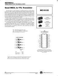
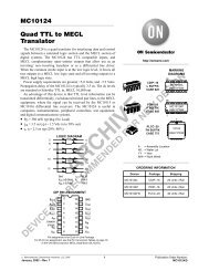
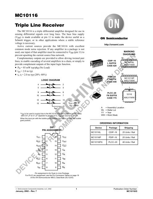
The <strong>MC10116</strong> is a triple differential amplifier designed for use insensing differential signals over long lines. The base bias supply(V BB ) is made available at pin 11 to make the device useful as aSchmitt trigger, or in other applications where a stable referencevoltage is necessary.Active current sources provide the <strong>MC10116</strong> with excellentcommon mode noise rejection. If any amplifier in a package is notused, one input of that amplifier must be connected to V BB (pin 11) toprevent upsetting the current source bias network.Complementary outputs are provided to allow driving twisted pairlines, to enable cascading of several amplifiers in a chain, or simply toprovide complement outputs of the input logic function.• P D = 85 mW typ/pkg (No Load)• t pd = 2.0 ns typ• t r , t f = 2.0 ns typ (20%–80%)LOGIC DIAGRAM *V BB to be used to supply bias to the <strong>MC10116</strong> only and bypassed (when used)with 0.01 µF to 0.1 µF capacitor to ground (0 V). V BB can source < 1.0 mA.When the input pin with the bubble goes positive, the output pin with the bubblegoes positive.DIPPIN ASSIGNMENThttp://onsemi.comCDIP–16L SUFFIXCASE 620PDIP–16P SUFFIXCASE 648PLCC–20FN SUFFIXCASE 77516ORDERING INFORMATI<strong>ON</strong>Device Package Shipping<strong>MC10116</strong>L CDIP–16 25 Units / Rail116A = Assembly LocationWL = Wafer LotYY = YearWW = Work Week1MARKINGDIAGRAMS<strong>MC10116</strong>LAWLYYWW<strong>MC10116</strong>PAWLYYWW110116AWLYYWW <strong>MC10116</strong>P PDIP–16 25 Units / Rail <strong>MC10116</strong>FN PLCC–20 46 Units / Rail Pin assignment is for Dual–in–<strong>Line</strong> Package.For PLCC pin assignment, see the Pin Conversion Tables on page 18of the <strong>ON</strong> <strong>Semiconductor</strong> MECL Data Book (DL122/D).© <strong>Semiconductor</strong> Components Industries, LLC, 2002January, 2002 – Rev. 71 Publication Order Number:<strong>MC10116</strong>/D
<strong>MC10116</strong>ELECTRICAL CHARACTERISTICSCharacteristicSymbolTest LimitsPinUnder–30°C +25°C +85°CTest Min Max Min Typ Max Min Max UnitPower Supply Drain Current I E 8 23 17 21 23 mAdcInput Current I inH 4 150 95 95 µAdcOutput Voltage Logic 1 V OH 23Output Voltage Logic 0 V OL 23Threshold Voltage Logic 1 V OHA 23Threshold Voltage Logic 0 V OLA 23I CBO 4 1.5 1.0 1.0 µAdc–1.060–1.060–1.890–1.890–1.080–1.080–0.890–0.890–1.675–1.675–1.655–1.655–0.960–0.960–1.850–1.850–0.980–0.980–0.810–0.810–1.650–1.650–1.630–1.630–0.890–0.890–1.825–1.825–0.910–0.910–0.700–0.700–1.615–1.615–1.595–1.595Reference Voltage V BB 11 –1.420 –1.280 –1.350 –1.230 –1.295 –1.150 VdcSwitching Times (50Ω Load)2Propagation Delay t 4+2+t 4–3+ 3t 4–2–t 4+3–23Rise Time (20 to 80%) t 2+ 2t 3+ 3Fall Time (20 to 80%) t 2– 2t 3– 31.01.01.01.01.11.11.11.13.13.13.13.13.63.63.63.61.01.01.01.01.11.11.11.12.02.02.02.02.02.02.02.02.92.92.92.93.33.33.33.31.01.01.01.01.11.11.11.13.33.33.33.33.73.73.73.7VdcVdcVdcVdcnshttp://onsemi.com2
<strong>MC10116</strong>ELECTRICAL CHARACTERISTICS (continued)TEST VOLTAGE VALUES (Volts)Characteristic@ Test Temperature V IHmax V ILmin V IHAmin V ILAmax V BB V EESymbol–30°C –0.890 –1.890 –1.205 –1.500+25°C –0.810 –1.850 –1.105 –1.475+85°C –0.700 –1.825 –1.035 –1.440From–5.2Pin–5.211–5.2Pin TEST VOLTAGE APPLIED TO PINS LISTED BELOWUnder(V CC )Test V IHmax V ILmin V IHAmin V ILAmax V BB V EE GndPower Supply Drain Current I E 8 4, 9, 12 5, 10, 13 8 1, 16Input Current I inH 4 4 9, 12 5, 10, 13 8 1, 16Output Voltage Logic 1 V OH 23Output Voltage Logic 0 V OL 23I CBO 4 9, 12 5, 10, 13 8,4 1, 1649, 129, 124Threshold Voltage Logic 1 V OHA 23 9, 12Threshold Voltage Logic 0 V OLA 23 9, 129, 12449, 129, 12 49, 12445, 10, 135, 10, 135, 10, 135, 10, 135, 10, 135, 10, 134 5, 10, 135, 10, 13Reference Voltage V BB 11 5, 10, 13 8 1, 16Switching Times (50Ω Load) Pulse In Pulse Out –3.2 V +2.0 V2Propagation Delay t 4+2+t 4–3+ 3t 4–2–t 4+3–23Rise Time (20 to 80%) t 2+ 2t 3+ 3Fall Time (20 to 80%) t 2– 2t 3– 344444444223323235, 10, 135, 10, 135, 10, 135, 10, 135, 10, 135, 10, 135, 10, 135, 10, 13Each MECL 10,000 series circuit has been designed to meet the dc specifications shown in the test table, after thermal equilibrium has beenestablished. The circuit is in a test socket or mounted on a printed circuit board and transverse air flow greater than 500 linear fpm is maintained.Outputs are terminated through a 50-ohm resistor to –2.0 volts. Test procedures are shown for only one gate. The other gates are tested in thesame manner.88888888888888881, 161, 161, 161, 161, 161, 161, 161, 161, 161, 161, 161, 161, 161, 161, 161, 16http://onsemi.com3
<strong>MC10116</strong>PACKAGE DIMENSI<strong>ON</strong>SPLCC–20FN SUFFIXPLASTIC PLCC PACKAGECASE 775–02ISSUE CB –N–Y BRKU D–L––M–ZWDXG1 VVIEW D–DZAR K1H C GG1EJ –T– VIEW S VIEW S KF http://onsemi.com4
<strong>MC10116</strong>Noteshttp://onsemi.com6
<strong>MC10116</strong>Noteshttp://onsemi.com7