Animating the Datapath Animating the Datapath: R-type Instruction ...
Animating the Datapath Animating the Datapath: R-type Instruction ...
Animating the Datapath Animating the Datapath: R-type Instruction ...

You also want an ePaper? Increase the reach of your titles
YUMPU automatically turns print PDFs into web optimized ePapers that Google loves.
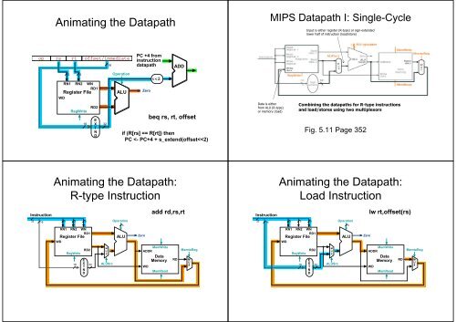
<strong>Animating</strong> <strong>the</strong> <strong>Datapath</strong>MIPS <strong>Datapath</strong> I: Single-CycleInput is ei<strong>the</strong>r register (R-<strong>type</strong>) or sign-extendedlower half of instruction (load/store)op rs rt offset/immediate5 5RN1 RN2 WNRD1Register FileWDRegWriteRD216EXTND3216OperationALUPC +4 frominstructiondatapathZero
<strong>Instruction</strong>3216<strong>Animating</strong> <strong>the</strong> <strong>Datapath</strong>:Store <strong>Instruction</strong>5 5RN1 RN2 WNRD1Register FileWDRegWrite5RD2E16 X 32 TNDMUXALUSrcOperation3ALUsw rt,offset(rs)ZeroMemWriteADDRDataMemoryWDMemReadRDMemtoRegMUXMIPS <strong>Datapath</strong> II: Single-CyclePC4Readaddress<strong>Instruction</strong><strong>Instruction</strong>memoryAddSeparate instruction memoryas instruction and data readoccur in <strong>the</strong> same clock cycleSeparate adder as ALU operations and PCincrement occur in <strong>the</strong> same clock cycleReadregister 1Readregister 2WriteregisterWritedataRegWriteRegistersReaddata 1Readdata 216 Sign 32extendALUSrcMuxAdding instruction fetch3ALU operationZeroALU ALUresultAddressWritedataMemReadMemWriteReaddataDatamemoryMemtoRegMuxMIPS <strong>Datapath</strong> III: Single-Cycle<strong>Datapath</strong> Executing addadd rd, rs, rtPCSrcNew multiplexorPC4ReadaddressAdd<strong>Instruction</strong><strong>Instruction</strong>memory<strong>Instruction</strong> address is ei<strong>the</strong>rPC+4 or branch target addressReadregister 1Readregister 2WriteregisterWritedataRegistersReaddata 1Readdata 2RegWrite16Sign32extendShiftleft 2ALUSrcMuxAdd ALUresultMuxExtra adder needed as bothadders operate in each cycle3 ALU operationMemWriteZeroALU ALUresultAddressWritedataMemReadReaddataDatamemoryMemtoRegMuxPC4ADDADDR<strong>Instruction</strong>MemoryRD<strong>Instruction</strong>32165 5RN1 RN2 WNRD1Register FileWDRegWrite5RD216EXTND32
<strong>Datapath</strong> Executing lwlw rt,offset(rs)<strong>Datapath</strong> Executing swsw rt,offset(rs)ADDADD4ADDMUX4ADDMUXPCADDR<strong>Instruction</strong>MemoryRD<strong>Instruction</strong>32165 5RN1 RN2 WNRD1Register FileWDRegWrite5RD216EXTND32
ALU Control• Plan to control ALU: main control sends a 2-bit ALUOp control field to<strong>the</strong> ALU control. Based on ALUOp and funct field of instruction <strong>the</strong>ALU control generates <strong>the</strong> 3-bit ALU control fieldRecall from Ch. 4– ALU control Funcfieldtion000 and001 or010 add110 sub111 sltMainControlALUControl• ALU must perform– add for load/stores (ALUOp 00)– sub for branches (ALUOp 01)– one of and, or, add, sub, slt for R-<strong>type</strong> instructions, depending on <strong>the</strong>instruction’s 6-bit funct field (ALUOp 10)6<strong>Instruction</strong>funct field2ALUOpALUOp generationby main control3ALUcontrolinputToALUSetting ALU Control Bits<strong>Instruction</strong> AluOp <strong>Instruction</strong> Funct Field Desired ALU controlopcodeoperation ALU action inputLW 00 load word xxxxxx add 010SW 00 store word xxxxxx add 010Branch eq 01 branch eq xxxxxx subtract 110R-<strong>type</strong> 10 add 100000 add 010R-<strong>type</strong> 10 subtract 100010 subtract 110R-<strong>type</strong> 10 AND 100100 and 000R-<strong>type</strong> 10 OR 100101 or 001R-<strong>type</strong> 10 set on less 101010 set on less 111*Typo in textFig. 5.15: if it is X<strong>the</strong>n <strong>the</strong>re is potentialconflict betweenline 2 and lines 3-7!ALUOp Funct field OperationALUOp1 ALUOp0 F5 F4 F3 F2 F1 F00 0 X X X X X X 0100*1 X X X X X X 1101 X X X 0 0 0 0 0101 X X X 0 0 1 0 1101 X X X 0 1 0 0 0001 X X X 0 1 0 1 0011 X X X 1 0 1 0 111Truth table for ALU control bitsDesigning <strong>the</strong> Main Control<strong>Datapath</strong> with Control IPCSrcR-<strong>type</strong>Load/storeor branchopcode31-26 25-21 20-16 15-11 10-6 5-0opcodersrsrtrtrd shamt functaddress31-26 25-21 20-16 15-0• Observations about MIPS instruction format– opcode is always in bits 31-26– two registers to be read are always rs (bits 25-21) and rt (bits 20-16)– base register for load/stores is always rs (bits 25-21)– 16-bit offset for branch equal and load/store is always bits 15-0– destination register for loads is in bits 20-16 (rt) while for R-<strong>type</strong>instructions it is in bits 15-11 (rd) (will require multiplexor to select)PC4AddReadaddress<strong>Instruction</strong>[31– 0]<strong>Instruction</strong>memoryNew multiplexor<strong>Instruction</strong> [25– 21]<strong>Instruction</strong> [20– 16]1Mu<strong>Instruction</strong> [15– 11] x0RegDst<strong>Instruction</strong> [15– 0]WriteregisterWritedataRegWriteReadregister 1Readregister 2Readdata 1Readdata 2Registers16 Sign 32extend<strong>Instruction</strong> [5– 0]Shiftleft 2ALUSrc1Mux0ALUcontrolALUOpALUAddresultZeroALU ALUresult1Mux0MemWriteAddressWritedataDatamemoryMemReadReaddataMemtoRegAdding control to <strong>the</strong> MIPS <strong>Datapath</strong> III (and a new multiplexor to select field tospecify destination register): what are <strong>the</strong> functions of <strong>the</strong> control signals?1Mux0
Control Signals<strong>Datapath</strong> with Control II0Signal Name Effect when deassertedEffect when assertedRegDst The register destination number for <strong>the</strong> The register destination number for <strong>the</strong>Write register comes from <strong>the</strong> rt field (bits 20-16) Write register comes from <strong>the</strong> rd field (bits 15-11)RegWrite None The register on <strong>the</strong> Write register input is writtenwith <strong>the</strong> value on <strong>the</strong> Write data inputAlLUSrc The second ALU operand comes from <strong>the</strong> The second ALU operand is <strong>the</strong> sign-extended,second register file output (Read data 2) lower 16 bits of <strong>the</strong> instructionPCSrc The PC is replaced by <strong>the</strong> output of <strong>the</strong> adder The PC is replaced by <strong>the</strong> output of <strong>the</strong> adderthat computes <strong>the</strong> value of PC + 4that computes <strong>the</strong> branch targetMemRead None Data memory contents designated by <strong>the</strong> addressinput are put on <strong>the</strong> first Read data outputMemWrite None Data memory contents designated by <strong>the</strong> addressinput are replaced by <strong>the</strong> value of <strong>the</strong> Write data inputMemtoReg The value fed to <strong>the</strong> register Write data input The value fed to <strong>the</strong> register Write data inputcomes from <strong>the</strong> ALUcomes from <strong>the</strong> data memoryPC4Readaddress<strong>Instruction</strong>memoryAdd<strong>Instruction</strong>[31– 0]<strong>Instruction</strong> [31 26]<strong>Instruction</strong> [25 21]<strong>Instruction</strong> [20 16]<strong>Instruction</strong> [15 11]<strong>Instruction</strong> [15 0]Control0Mux1RegDstBranchMemReadMemtoRegALUOpMemWriteALUSrcRegWriteReadregister 1Readdata 1Readregister 2Registers ReadWrite data 2registerWritedata16 32SignextendShiftleft 20Mux1ALUcontrolAddresultALUZeroALU ALUresultWritedataMux1AddressPCSrcDatamemoryReaddata1Mux0Effects of <strong>the</strong> seven control signals<strong>Instruction</strong> [5 0]MIPS datapath with <strong>the</strong> control unit: input to control is <strong>the</strong> 6-bit instructionopcode field, output is seven 1-bit signals and <strong>the</strong> 2-bit ALUOp signal4AddRegDstBranchMemReadShiftleft 2AddALUresult0Mux1PCSrcPCSrc cannot beset directly from <strong>the</strong>opcode: zero testoutcome is requiredControl Signals:R-Type <strong>Instruction</strong><strong>Instruction</strong> [31 26]MemtoRegControlALUOpMemWriteALUSrcRegWritePCReadaddress<strong>Instruction</strong>memory<strong>Instruction</strong>[31– 0]<strong>Instruction</strong> [25 21]<strong>Instruction</strong> [20 16]<strong>Instruction</strong> [15 11]<strong>Instruction</strong> [15 0]0Mux1Readregister 1Readregister 2RegistersWriteregisterWritedata<strong>Instruction</strong> [5 0]16 32Signextend<strong>Instruction</strong> RegDst ALUSrcMemto-RegRegWriteMemReadMemWrite Branch ALUOp1 ALUp0R-format 1 0 0 1 0 0 0 1 0lw 0 1 1 1 1 0 0 0 0sw X 1 X 0 0 1 0 0 0beq X 0 X 0 0 0 1 0 1Readdata 1Readdata 20Mux1ALUcontrolZeroALU ALUresultDetermining control signals for <strong>the</strong> MIPS datapath based on instruction opcodeAddressWritedataDatamemoryReaddata1Mux0PC4ADDADDR RD<strong>Instruction</strong>Memoryimmediate/offsetI[15:0]Control signalsshown in blue<strong>Instruction</strong>I 3216rsI[25:21]rtI[20:16]5 5RN1 RN2 WNRD1Register FileWDRegWrite10rdI[15:11]5MUX5RD21E16 X 32TND10???RegDstOperation01MUXALUSrc
Drag‐and‐drop programmingTeachers have quickly realized that adding actionable objects in lessons is a great way of creating even moreinteresting and intriguing activities for your students. You will find that ActivInspire makes it easier and quickerthrough a new Drag‐and‐Drop option.Open your Browser by choosing View > Browser, and clicking on <strong>the</strong> Action Browser icon as indicated by <strong>the</strong> redarrow below. Next, click on <strong>the</strong> Drag‐and‐Drop tab. If you want to make something interactive, just drag <strong>the</strong>function you want <strong>the</strong> software to do onto <strong>the</strong> flipchart. Drop it on <strong>the</strong> page and an icon will <strong>the</strong>n appear withthat action ready to click.If you drop <strong>the</strong> action item on top of an object, <strong>the</strong>n that object will carry out <strong>the</strong> assigned action. For example,you can drag <strong>the</strong> Notes Browser onto <strong>the</strong> question mark shown on <strong>the</strong> flipchart page below, or drag <strong>the</strong> NextPage onto <strong>the</strong> blue arrow. When you click on ei<strong>the</strong>r one, <strong>the</strong> appropriate action will occur.Quick Tip: If you want to add an action to an object on <strong>the</strong> page and your browser window is not open, you canquickly bring up <strong>the</strong> Action browser by choosing <strong>the</strong> object and its Object Edit menu, and selecting ActionBrowser! Then drag your action onto <strong>the</strong> object!Creating interactive lessons couldn’t be easier, or faster!9
Step 2: <strong>Instruction</strong> Decode andRegister Fetch (ID)• Read registers rs and rt in case we need <strong>the</strong>m.Compute <strong>the</strong> branch address in case <strong>the</strong> instruction is a branch.• RTL:A = Reg[IR[25-21]];B = Reg[IR[20-16]];ALUOut = PC + (sign-extend(IR[15-0])
Multicycle <strong>Datapath</strong> with Control IINew gatesFor <strong>the</strong> jump addressNew multiplexorMulticycle Control Step (1):FetchPCWriteCondPCWriteIorDMemReadMemWriteMemtoRegOutputsControlPCSourceALUOpALUSrcBALUSrcARegWriteIR = Memory[PC];PC = PC + 4; 1IRWritePC0Mux1AddressWritedataMemoryMemData<strong>Instruction</strong>[31-26]<strong>Instruction</strong>[25– 21]<strong>Instruction</strong>[20– 16]<strong>Instruction</strong>[15– 0]<strong>Instruction</strong>register<strong>Instruction</strong>[15– 0]MemorydataregisterIRWrite<strong>Instruction</strong> [25– 0]<strong>Instruction</strong>[15– 11]Op[5– 0]0Mux10Mux1RegDst16Readregister 1Readregister 2WriteregisterWritedataRegistersSignextendComplete multicycle MIPS datapath (with branch and jump capability)and showing <strong>the</strong> main control block and all control linesReaddata 1Readdata 232<strong>Instruction</strong> [5– 0]Shiftleft 2AB401 Mu2 x30Mux126 28ShiftALUcontrolleft 2PC [31-28]ZeroALU ALUresultJumpaddress [31-0]ALUOut012Mux1PCWr*PC0IorD0 MU1 X0MemWriteADDRMemoryWDMemRead1RDIRMDR<strong>Instruction</strong> I321 MU0 XMemtoRegXimmediatersrt5 5RN1 RN2 WNRegisters RD1WDRegWrite0E16 X 32TNDjmpaddrI[25:0]5rd0MUX1 RegDst5RD2
Multicycle Control Step (3):ALU <strong>Instruction</strong> (R-Type)Multicycle Control Step (3):Branch <strong>Instruction</strong>sALUOut = A op B;0IRWriteif (A == B) PC = ALUOut;0IRWrite0PCWr*PCXIorD0 MU1 XMemWriteADDRMemoryWDMemRead00 132RegDst5 5 MUX5 X10RDIRMDR<strong>Instruction</strong> I1 MU0 XMemtoRegXimmediatersrtRN1 RN2 WNRegisters RD1WDRegWrite0E16 X 32TND5RD2jmpaddrI[25:0]rd
Multicycle Execution Steps (4)Memory Access - Write (sw)Memory[ALUOut] = B;IRWrite0Multicycle Control Step (4):ALU <strong>Instruction</strong> (R-Type)Reg[IR[15:11]] = ALUOut; (Reg[Rd] =ALUOut) 0IRWrite0PCWr*PC1IorD0 MU1 XMemWriteADDRMemoryWDMemRead10321 RegDst5 5 MUX5 XX0RDIRMDR<strong>Instruction</strong> I1 MU0 XMemtoRegXimmediatersrtRN1 RN2 WNRegisters RD1WDRegWrite0E16 X 32TND5RD2jmpaddrI[25:0]rd
Implementing ControlReview: Finite State Machines• Value of control signals is dependent upon:– what instruction is being executed– which step is being performed• Finite state machines (FSMs):– a set of states and– next state function, determined by current state and <strong>the</strong> input– output function, determined by current state and possibly input• Use <strong>the</strong> information we have accumulated to specify a finitestate machine– specify <strong>the</strong> finite state machine graphically, or– use microprogrammingInputsCurrent stateClockNext-statefunctionNextstate• Implementation is <strong>the</strong>n derived from <strong>the</strong> specificationOutputfunctionOutputs– We’ll use a Moore machine – output based only on current stateStartExample: Moore Machine• The Moore machine below, given input a binary stringterminated by “#”, will output “even” if <strong>the</strong> string has an evennumber of 0’s and “odd” if <strong>the</strong> string has an odd number of 0’s1Even stateNooutputOutput“even”00Odd stateNooutput# #Output“odd”1FSM Control: High-level ViewAsserted signalsshown insidestate circlesMemory accessinstructions(Figure 5.38)StartStartMemory reference FSM(Figure 5.38)<strong>Instruction</strong> fetch/decode and register fetch(Figure 5.37)R-<strong>type</strong> instructions(Figure 5.39)Branch instruction(Figure 5.40)High-level view of FSM control(Op = 'LW') or (Op = 'SW')<strong>Instruction</strong> fetch0MemReadALUSrcA = 0IorD = 0IRWriteALUSrcB = 01ALUOp = 00PCWritePCSource = 00R-<strong>type</strong> FSM(Figure 5.39)(Op = R-<strong>type</strong>)Branch FSM(Figure 5.40)Jump instruction(Figure 5.41)(Op = 'BEQ')<strong>Instruction</strong> decode/Register fetch1ALUSrcA = 0ALUSrcB = 11ALUOp = 00(Op = 'JMP')Jump FSM(Figure 5.41)Output even stateOutput odd state<strong>Instruction</strong> fetch and decode steps of every instruction is identical
FSM Control: Memory Reference2From state 1ALUSrcA = 1ALUSrcB = 10ALUOp = 00(Op = 'LW') or (Op = 'SW')Memory address computationFSM Control: R-<strong>type</strong> <strong>Instruction</strong>From state 1(Op = R-<strong>type</strong>)Execution63(Op = 'LW')Memoryaccess(Op = 'SW')5MemoryaccessALUSrcA = 1ALUSrcB = 00ALUOp = 104MemReadIorD = 1Write-back stepMemWriteIorD = 17RegDst = 1RegWriteMemtoReg = 0R-<strong>type</strong> completionRegWriteMemtoReg = 1RegDst = 0To state 0(Figure 5.37)FSM control for memory-reference has 4 statesTo state 0(Figure 5.37)FSM control to implement R-<strong>type</strong> instructions has 2 statesFSM Control: Branch <strong>Instruction</strong>FSM Control: Jump <strong>Instruction</strong>8From state 1(Op = 'BEQ')ALUSrcA = 1ALUSrcB = 00ALUOp = 01PCWriteCondPCSource = 01Branch completion9From state 1(Op = 'J')PCWritePCSource = 10Jump completionTo state 0(Figure 5.37)FSM control to implement branches has 1 stateTo state 0(Figure 5.37)FSM control to implement jumps has 1 state
EXMEMWB23FSM Control: Complete View4Memory addresscomputationALUSrcA = 1ALUSrcB = 10ALUOp = 00(Op = 'LW')MemReadIorD = 1MemoryaccessRegDst = 0RegWriteMemtoReg =1(Op = 'SW')5Write-back stepStart(Op = 'LW') or (Op = 'SW')MemWriteIorD = 1IFMemoryaccess67<strong>Instruction</strong> fetch0MemReadALUSrcA = 0IorD = 0IRWriteALUSrcB = 01ALUOp = 00PCWritePCSource = 00ExecutionALUSrcA =1ALUSrcB = 00ALUOp= 10RegDst = 1RegWriteMemtoReg = 08R-<strong>type</strong> completion(Op = R-<strong>type</strong>)BranchcompletionIDALUSrcA = 1ALUSrcB = 00ALUOp = 01PCWriteCondPCSource = 01(Op = 'BEQ')<strong>Instruction</strong> decode/register fetch19ALUSrcA = 0ALUSrcB = 11ALUOp = 00(Op = 'J')JumpcompletionPCWritePCSource = 10Labels on arcs are conditionsthat determine next stateThe complete FSM control for <strong>the</strong> multicycle MIPS datapath:refer Multicycle <strong>Datapath</strong> with Control IIExample: CPI in a multicycleCPU• Assume– <strong>the</strong> control design of <strong>the</strong> previous slide– An instruction mix of 22% loads, 11% stores, 49% R-<strong>type</strong> operations,16% branches, and 2% jumps• What is <strong>the</strong> CPI assuming each step requires 1 clock cycle?• Solution:– Number of clock cycles from previous slide for each instruction class:• loads 5, stores 4, R-<strong>type</strong> instructions 4, branches 3, jumps 3– CPI = CPU clock cycles / instruction count= Σ (instruction count class i× CPI class i) / instruction count= Σ (instruction count class I/ instruction count) × CPI class I= 0.22 × 5 + 0.11 × 4 + 0.49 × 4 + 0.16 × 3 + 0.02 × 3= 4.04FSM Control:ImplementationOp5Op4Op3PCWritePCWriteCondIorDMemReadMemtoRegPCSourceALUOpALUSrcBALUSrcARegWriteRegDstHigh-level view of FSM implementation: inputs to <strong>the</strong> combinational logic block are<strong>the</strong> current state number and instruction opcode bits; outputs are <strong>the</strong> next statenumber and control signals to be asserted for <strong>the</strong> current stateOp2Op1<strong>Instruction</strong> registeropcode fieldControl logicInputsOp0Four state bits are required for 10 statesS3S2OutputsS1S0State registerMemWriteIRWriteNS3NS2NS1NS0FSMControl:PLAImplementationOp5Op4Op3Op2Op1Op0S3S2S1S0PCWritePCWriteCondIorDMemReadMemWriteIRWriteMemtoRegPCSource1PCSource0ALUOp1ALUOp0ALUSrcB1ALUSrcB0ALUSrcARegWriteRegDstNS3NS2NS1Upper half is <strong>the</strong> AND plane that computes all <strong>the</strong> products. The products are carriedto <strong>the</strong> lower OR plane by <strong>the</strong> vertical lines. The sum terms for each output is given by<strong>the</strong> corresponding horizontal lineE.g., IorD = S0.S1.S2.S3 + S0.S1.S2.S3NS0
FSM Control: ROMImplementation• ROM (Read Only Memory)– values of memory locations are fixed ahead of time• A ROM can be used to implement a truth table– if <strong>the</strong> address is m-bits, we can address 2 m entries in <strong>the</strong> ROM– outputs are <strong>the</strong> bits of <strong>the</strong> entry <strong>the</strong> address points tomnROM m = 3n = 4address output0 0 0 0 0 1 10 0 1 1 1 0 00 1 0 1 1 0 00 1 1 1 0 0 01 0 0 0 0 0 01 0 1 0 0 0 11 1 0 0 1 1 01 1 1 0 1 1 1The size of an m-input n-output ROM is 2 m x n bits – such a ROM canbe thought of as an array of size 2 m with each entry in <strong>the</strong> array beingn bitsFSM Control: ROM vs. PLA• First improve <strong>the</strong> ROM: break <strong>the</strong> table into two parts– 4 state bits give <strong>the</strong> 16 output signals – 2 4 x 16 bits of ROM– all 10 input bits give <strong>the</strong> 4 next state bits – 2 10 x 4 bits of ROM– Total – 4.3K bits of ROM• PLA is much smaller– can share product terms– only need entries that produce an active output– can take into account don't cares• PLA size = (#inputs ´ #product-terms) + (#outputs ´ #productterms)– FSM control PLA = (10x17)+(20x17) = 460 PLA cells• PLA cells usually about <strong>the</strong> size of a ROM cell (slightly bigger)Microprogramming• Microprogramming is a method of specifying FSM control thatresembles a programming language – textual ra<strong>the</strong>r graphic– this is appropriate when <strong>the</strong> FSM becomes very large, e.g., if <strong>the</strong>instruction set is large and/or <strong>the</strong> number of cycles per instructionis large– in such situations graphical representation becomes difficult as<strong>the</strong>re may be thousands of states and even more arcs joining <strong>the</strong>m– a microprogram is specification : implementation is by ROM or PLA• A microprogram is a sequence of microinstructions– each microinstruction has eight fields (label + 7 functional)• Label: used to control microcode sequencing• ALU control: specify operation to be done by ALU• SRC1: specify source for first ALU operand• SRC2: specify source for second ALU operand• Register control: specify read/write for register file• Memory: specify read/write for memory• PCWrite control: specify <strong>the</strong> writing of <strong>the</strong> PC• Sequencing: specify choice of next microinstructionMicroprogramming• The Sequencing field value determines <strong>the</strong> execution order of<strong>the</strong> microprogram– value Seq : control passes to <strong>the</strong> sequentially next microinstruction– value Fetch : branch to <strong>the</strong> first microinstruction to begin <strong>the</strong> nextMIPS instruction, i.e., <strong>the</strong> first microinstruction in <strong>the</strong> microprogram– value Dispatch i : branch to a microinstruction based on controlinput and a dispatch table entry (called dispatching):• Dispatching is implemented by means of creating a table, calleddispatch table, whose entries are microinstruction labels and which isindexed by <strong>the</strong> control input. There may be multiple dispatch tables –<strong>the</strong> value Dispatch i in <strong>the</strong> sequencing field indicates that <strong>the</strong> i thdispatch table is to be used
Control Microprogram• The microprogram corresponding to <strong>the</strong> FSM control showngraphically earlier:LabelALUcontrol SRC1 SRC2Registercontrol M em oryPCW ritecontrol SequencingFetch Add PC 4 Read PC ALU SeqAdd PC Extshft Read Dispatch 1M em 1 Add A Extend Dispatch 2LW 2 Read ALU SeqW rite M DRFetchSW 2 W rite ALU FetchRform at1 Func code A B SeqW rite ALUFetchBEQ 1 Subt A B ALUO ut-cond FetchJUM P1 Jum p address FetchMicroprogram containing 10 microinstructionsDispatch ROM 1Op Opcode name Value000000 R-format Rformat1000010 jmp JUMP1000100 beq BEQ1100011 lw Mem1101011 sw Mem1Dispatch Table 1Dispatch ROM 2Op Opcode name Value100011 lw LW2101011 sw SW2Dispatch Table 2Microcode: Trade-offs• Specification advantages– easy to design and write– typically manufacturer designs architecture and microcode in parallel• Implementation advantages– easy to change since values are in memory (e.g., off-chip ROM)– can emulate o<strong>the</strong>r architectures– can make use of internal registers• Implementation disadvantages– control is implemented nowadays on same chip as processor so <strong>the</strong>advantage of an off-chip ROM does not exist– ROM is no longer faster than on-board cache– <strong>the</strong>re is little need to change <strong>the</strong> microcode as general-purposecomputers are used far more nowadays than computers designed forspecific applicationsSummary• Techniques described in this chapter to design datapaths andcontrol are at <strong>the</strong> core of all modern computer architecture• Multicycle datapaths offer two great advantages over single-cycle– functional units can be reused within a single instruction if <strong>the</strong>y areaccessed in different cycles – reducing <strong>the</strong> need to replicate expensivelogic– instructions with shorter execution paths can complete quicker byconsuming fewer cycles• Modern computers, in fact, take <strong>the</strong> multicycle paradigm to a higherlevel to achieve greater instruction throughput:– pipelining (next topic) where multiple instructions executesimultaneously by having cycles of different instructions overlap in <strong>the</strong>datapath– <strong>the</strong> MIPS architecture was designed to be pipelined