PIC16f877 & Analog-to-digital converter module
PIC16f877 & Analog-to-digital converter module
PIC16f877 & Analog-to-digital converter module

Create successful ePaper yourself
Turn your PDF publications into a flip-book with our unique Google optimized e-Paper software.
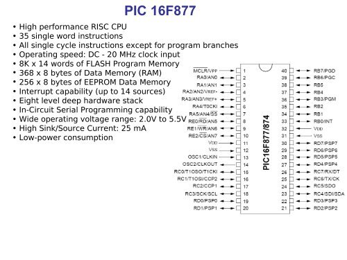
PIC 16F877• High performance RISC CPU• 35 single word instructions• All single cycle instructions except for program branches• Operating speed: DC - 20 MHz clock input• 8K x 14 words of FLASH Program Memory• 368 x 8 bytes of Data Memory (RAM)• 256 x 8 bytes of EEPROM Data Memory• Interrupt capability (up <strong>to</strong> 14 sources)• Eight level deep hardware stack• In-Circuit Serial Programming capability• Wide operating voltage range: 2.0V <strong>to</strong> 5.5V• High Sink/Source Current: 25 mA• Low-power consumption
PIC 16F877
PIC 16F877Program Memory Organization• PIC16F877 has a 13-bit PC• PIC16F877 has 8K x 14 words ofFLASH program memory, and the• Accessing a location above thephysically implemented address willcause a wraparound.• The RESET vec<strong>to</strong>r is at 0000h and theinterrupt vec<strong>to</strong>r is at 0004h.
PIC 16F877Data Memory Organization• The data memory is partitioned in<strong>to</strong>multiple banks which contain theGeneral Purpose Registers and theSpecial Function Registers.• Bits RP1 (STATUS) and RP0(STATUS) are the bank selectbits.
PIC 16F877: A/D Converter Module• 10-bit resolution• 8 inputs• Successive approximation A/D <strong>converter</strong>• Selectable voltage reference sources (VDD, VSS, RA2, RA3)• The A/D <strong>module</strong> has four registers.- A/D Control Register0 (ADCON0) Control operation- A/D Control Register1 (ADCON1) Config port pins- A/D Result High Register (ADRESH) S<strong>to</strong>re result- A/D Result Low Register (ADRESL) S<strong>to</strong>re result
PIC 16F877: A/D Module• ADCS1:ADCS0: A/D Conversion Clock Select bits00 = FOSC/201 = FOSC/810 = FOSC/3211 = FRC (clock derived from the internal A/D <strong>module</strong> RC oscilla<strong>to</strong>r)• CHS2:CHS0: <strong>Analog</strong> Channel Select bits000 = channel 0, (RA0/AN0)001 = channel 1, (RA1/AN1)010 = channel 2, (RA2/AN2)011 = channel 3, (RA3/AN3)100 = channel 4, (RA5/AN4)101 = channel 5, (RE0/AN5)(1)110 = channel 6, (RE1/AN6)(1)111 = channel 7, (RE2/AN7)(1)
PIC 16F877: A/D Module• GO/DONE: A/D Conversion Status bitIf ADON = 1:1 = A/D conversion in progress (setting this bit starts the A/Dconversion)0 = A/D conversion not in progress (this bit is au<strong>to</strong>matically clearedby hardware when the A/D conversion is complete)• ADON: A/D On bit1 = A/D <strong>converter</strong> <strong>module</strong> is operating0 = A/D <strong>converter</strong> <strong>module</strong> is shut-off and consumes no operatingcurrent
PIC 16F877: A/D Module• ADFM: A/D Result Format Select bit1 = Right justified. 6 Most Significant bits of ADRESH are read as ‘0’.0 = Left justified. 6 Least Significant bits of ADRESL are read as ‘0’.• PCFG3:PCFG0: A/D Port Configuration Control bits:
PIC 16F877 : A/D Module
PIC 16F877 : A/D Module• The ADRESH:ADRESL registers contain the 10-bit result of the A/Dconversion.• When the A/D conversion is complete, the result is loaded in<strong>to</strong> this A/Dresult register pair.• The GO/DONE bit (ADCON0) is cleared• The A/D interrupt flag bit ADIF is set.• The analog input channels must have their corresponding TRIS bits setas inputs.
PIC 16F877 : A/D ModuleUsing A/D Module1. Configure the A/D <strong>module</strong>:• Configure analog pins/voltage reference and <strong>digital</strong> I/O (ADCON1)• Select A/D input channel (ADCON0)• Select A/D conversion clock (ADCON0)• Turn on A/D <strong>module</strong> (ADCON0)2. Configure A/D interrupt (if desired):• Clear ADIF bit• Set ADIE bit• Set PEIE bit• Set GIE bit3. Wait the required acquisition time.4. Start conversion:• Set GO/DONE bit (ADCON0)5. Wait for A/D conversion <strong>to</strong> complete, by either:• Polling for the GO/DONE bit <strong>to</strong> be cleared (with interruptsenabled); OR• Waiting for the A/D interrupt6. Read A/D result register pair (ADRESH:ADRESL), clear bit ADIF ifrequired.7. For the next conversion, go <strong>to</strong> step 1 or step 2, as required.
PIC 16F877 : A/D ModuleObtaining A/D results