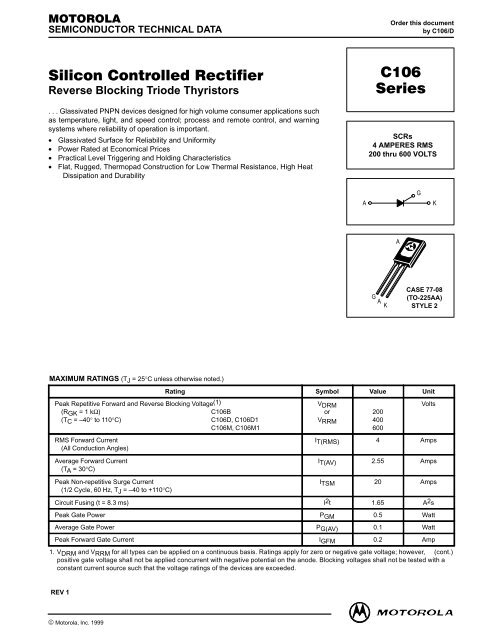
Silicon Controlled Rectifier C106 Series
Silicon Controlled Rectifier C106 Series
Silicon Controlled Rectifier C106 Series

You also want an ePaper? Increase the reach of your titles
YUMPU automatically turns print PDFs into web optimized ePapers that Google loves.
MAXIMUM RATINGS — continuedRating Symbol Value UnitPeak Reverse Gate Voltage VGRM 6 VoltsOperating Junction Temperature Range TJ –40 to +110 °CStorage Temperature Range Tstg –40 to +150 °CMounting Torque(1) — 6 in. lb.1. Torque rating applies with use of compression washer (B52200F006). Mounting torque in excess of 6 in. lb. does not appreciably lowercase-to-sink thermal resistance. Anode lead and heatsink contact pad are common.For soldering purposes (either terminal connection or device mounting), soldering temperatures shall not exceed +200°C. For optimumresults, an activated flux (oxide removing) is recommended.THERMAL CHARACTERISTICS (TC = 25°C, RGK = 1 kΩ unless otherwise noted.)Characteristic Symbol Max UnitThermal Resistance, Junction to Case RθJC 3 °C/WThermal Resistance, Junction to Ambient RθJA 75 °C/WELECTRICAL CHARACTERISTICS (TC = 25°C unless otherwise noted.)Characteristic Symbol Min Typ Max UnitPeak Forward or Reverse Blocking Current(VAK = Rated VDRM or VRRM, RGK = 1000 Ohms) TJ = 25°CTJ = 110°CForward “On” Voltage(IFM = 1 A Peak for <strong>C106</strong>B, D, & M)(IFM = 4 A Peak for <strong>C106</strong>D1, & M1)Gate Trigger Current (Continuous dc)(VAK = 6 Vdc, RL = 100 Ohms)(VAK = 6 Vdc, RL = 100 Ohms, TC = –40°C)Gate Trigger Voltage (Continuous dc)(VAK = 6 Vdc, RL = 100 Ohms, RGK = 1000 Ohms) TJ = 25°C(VAK = Rated VDRM, RL = 3000 Ohms,RGK = 1000 Ohms, TJ = 110°C)TJ = –40°CHolding Current TJ = 25°C(VD = 12 Vdc, RGK = 1000 Ohms)TJ = –40°CTJ = +110°CForward Voltage Application Rate(TJ = 110°C, RGK = 1000 Ohms, VD = Rated VDRM)IDRM, IRRM————10100µAµAVTM — — 2.2 VoltsIGTVGT——0.40.50.2IH 0.30.40.143075——————2005000.81—362µAVoltsmAdv/dt — 8 — V/µsTurn-On Time tgt — 1.2 — µsTurn-Off Time tq — 40 — µs2 Motorola Thyristor Device Data
T C , CASE TEMPERATURE ( ° C)11010090807060504030FIGURE 1 – AVERAGE CURRENT DERATINGHALF SINE WAVERESISTIVE OR INDUCTIVE LOAD.50 to 400 Hz20100 .4 .8 1.2 1.6 2.0 2.4 2.8 3.2IT(AV) AVERAGE ON-STATE CURRENT (AMPERES)DC3.64.0P (AV) , AVERAGE ON-STATE POWER DISSIPATION (WATTS)FIGURE 2 – MAXIMUM ON-STATE POWER DISSIPATION10864200HALF SINE WAVERESISTIVE OR INDUCTIVE LOAD50 TO 400Hz.JUNCTION TEMPERATURE ≈ 110°C.4 .8 1.2 1.6 2.0 2.4 2.6 3.2 3.6 4.0IT(AV) AVERAGE ON-STATE CURRENT (AMPERES)DCPackage InterchangeabilityThe dimensional diagrams below compare the critical dimensions of the Motorola C-106 packagewith competitive devices. It has been demonstrated that the smaller dimensions of the Motorolapackage make it compatible in most lead-mount and chassis-mount applications. The user isadvised to compare all critical dimensions for mounting compatibility.____ .145.155____ .295.305____ .115.130____ .095.105____ .135.115____ .400.360____ .127.123 DIA____ .026.019____ .148.158____ .425.4355 TYP____ .520.480____ .050.0951 2 3____ .575.655____ .385.365____ .420.400____ .315.285____ .020.026.040.094 BSC____ .025.035____ .015.025____ .045.055____ .105.095____ .054.046____ .105.095____ .190.170Motorola C-106 PackageCompetitive C-106 PackageMotorola Thyristor Device Data3