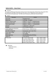
AN30888A High Brightness LED Driver IC - Panasonic
AN30888A High Brightness LED Driver IC - Panasonic
AN30888A High Brightness LED Driver IC - Panasonic
- No tags were found...

You also want an ePaper? Increase the reach of your titles
YUMPU automatically turns print PDFs into web optimized ePapers that Google loves.
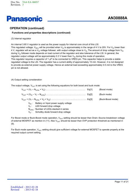
Established : 2012-02-28Revised : 2013-02-18Doc No. TA4-EA-06057Revision. 3Product Standards<strong>AN30888A</strong>OPERATION (continued)Functions and properties descriptions (continued)(3) Internal regulatorAn internal 3.65 V regulator is used as the power supply for internal core circuit of this LSI.This regulated voltage, V REG will be provided when V IN is approximately in the range of 4 V to 20V. For V IN lower than4 V, regulator will act as a V IN voltage follower, with output voltage close to V IN. The amount of drop voltage from V INduring V IN follower mode depends on load current of the regulator and also tolerance of the LSI. In general, theregulator output voltage will be approximately 0.3 V lower than V IN during this mode of operation.This regulator requires a capacitor of 1 µF to be connected to VREG pin. This capacitor helps to provide a stableregulated voltage to the LSI. The regulator has a current ability of approximately 15 mA. However, it is not designedto provide as external power supply voltage. Hence an external load exceeding approximately 0.5 mA to the VREGpin is not allowed.(4) Output setting considerationThe output voltage, V OUT is set using the following equations for both boost and buck mode:V OUT = (V F N <strong>LED</strong>s + V D ) ……………………………………………… Eq[1] (Boost mode)V OUT = (V IN –V F N <strong>LED</strong>s ) ……………………………………………… Eq[2] (Buck mode)V OUT = (V F N <strong>LED</strong>s + V D + V IN ) ………………………………………… Eq[3]V IN : Battery or Input power supply voltageV F : <strong>LED</strong> forward drop voltageN <strong>LED</strong>s : Number of <strong>LED</strong>s stacked in seriesV D : Schottky diode forward drop voltage(Buck-Boost mode)For Boost mode or Buck-Boost mode operation, V OUT setting should be lesser than Drain–Source breakdown voltageof external MOSFET as mention in (11). Also V OUT should be lesser than OVP protection threshold as mentioned in(9).For Buck mode operation, V OUT setting should give sufficient voltage for external MOSFET to operate properly at therequired output current setting.Page 11 of 21