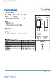
AN30888A High Brightness LED Driver IC - Panasonic
AN30888A High Brightness LED Driver IC - Panasonic
AN30888A High Brightness LED Driver IC - Panasonic
- No tags were found...

Create successful ePaper yourself
Turn your PDF publications into a flip-book with our unique Google optimized e-Paper software.
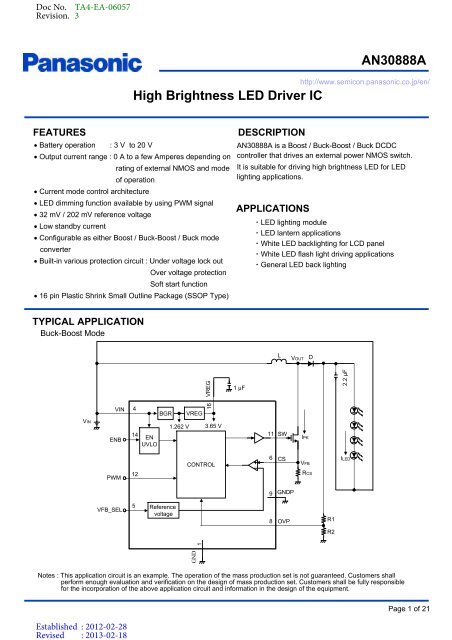
Established : 2012-02-28Revised : 2013-02-18Doc No. TA4-EA-06057Revision. 3Product Standards<strong>AN30888A</strong>TYP<strong>IC</strong>AL APPL<strong>IC</strong>ATION ( Continued )Buck ModeVREG1 µFD2.2 µFVIN4BGRVREG16LVINENB14ENUVLO1.262 V3.65 V11SWIPKCONTROL6CSVFBVOUTI<strong>LED</strong>PWM12RCS9GNDPVFB_SEL5Referencevoltage8OVPGND1Notes:This application circuit is an example. The operation of the mass production set is not guaranteed. Customers shallperform enough evaluation and verification on the design of mass production set. Customers shall be fullyresponsible for the incorporation of the above application circuit and information in the design of the equipment.Page 3 of 21
Established : 2012-02-28Revised : 2013-02-18Doc No. TA4-EA-06057Revision. 3Product Standards<strong>AN30888A</strong>ABSOLUTE MAXIMUM RATINGSParameterSymbolRatingUnitNoteSupply voltageV IN21V*1Output CurrentI OUT—mA*1Operating ambience temperatureT opr–25to+85C*2Operating junction temperatureT j–25to+125C*2Storage temperatureT stg–55to+125C*2CS, OVP– 0.3 to 4.3V—Input Voltage RangeVFB_SEL, PWM– 0.3 to 5.5V—ENB– 0.3 to 21V—Output Voltage RangeSW, VREG– 0.3 to 4.3V—ESDHBM (Human Body Model)2kV—Note)This product may sustain permanent damage if subjected to conditions higher than the above stated absolute maximumrating. This rating is the maximum rating and device operating at this range is not guaranteeable as it is higher than ourstated recommended operating range. When subjected under the absolute maximum rating for a long time, the reliability ofthe product may be affected.*1: V IN = VIN.The values under the condition not exceeding the above absolute maximum ratings and the power dissipation.*2: Except for the power dissipation, operating ambient temperature, and storage temperature, all ratings are for Ta =25C.POWER DISSIPATION RATINGPACKAGE JAPD (Ta=25 C)PD (Ta=85 C)16 pin Plastic Shrink Small Outline Package (SSOP Type)171.8 C /W0.582 W0.233 WNote)For the actual usage, please refer to the P D -Ta characteristics diagram in the package specification, supply voltage, loadand ambient temperature conditions to ensure that there is enough margin follow the power and the thermal design doesnot exceed the allowable value.CAUTIONAlthough this LSI has built-in ESD protection circuit, it may still sustain permanent damage if not handledproperly. Therefore, proper ESD precautions are recommended to avoid electrostatic damage to the MOSgates.Page 4 of 21
Established : 2012-02-28Revised : 2013-02-18Doc No. TA4-EA-06057Revision. 3Product Standards<strong>AN30888A</strong>RECOMMENDED OPERATING CONDITIONSParameterSupply voltage rangeInput Voltage RangeOutput Voltage RangeSymbolVIN1( Boost Mode / Buck – Boost Mode )VIN2( Buck Mode )V CS , V OVP33–0.366—1220VREGVFB_SEL, V PWM –0.3 — 5.2 V —V ENB –0.3 —VIN1orVIN2V *2–0.3 — 5.2 V —V SWVREGMin.–0.3Typ.—Max.4.0UnitVVVVNote*1*1*2—Note) *1: The values under the condition not exceeding the above absolute maximum ratings and the power dissipation.Do not apply external currents and voltages to any pin not specifically mentioned.Voltage values, unless otherwise specified, are with respect to GND. GND is voltage for GND and GNDP.VIN1 and VIN2 are voltage for VIN.*2: VREG V must not be exceeded 4.3 V. VIN1 V and VIN2 V must not be exceeded 21 V.Page 5 of 21
Established : 2012-02-28Revised : 2013-02-18Doc No. TA4-EA-06057Revision. 3Product Standards<strong>AN30888A</strong>ELECTR<strong>IC</strong>AL CHARACTERIST<strong>IC</strong>SV IN = 6 V, ENB = 6 V, PWM = V REGNote) T a = 25 C 2 C unless otherwise specified.ParameterSymbolConditionMinLimitsTypMaxUnitNoteCircuit Current ConsumptionStandby CurrentI STBENB = 0 V——10µA—Operating Quiescent CurrentENB Low Input LogicVFB_SEL <strong>High</strong> Input LogicVFB_SEL Low Input LogicPWM <strong>High</strong> input LogicPWM Low input LogicInput Pin Current ConsumptionEnable Pin CurrentOutput <strong>Driver</strong>SW <strong>High</strong> Output LogicSW Low Output LogicUnder Voltage Lock Out (UVLO)Under Voltage protection onvalueUnder voltage protectionHysteresisI CCV ENBLV VFBSELHV VFBSELLV PWMHV PWMLI ENBV SWHV SWLV UVLOONV UVLOHYSENB = V INNo load conditionENABLE (ENB), VFB_SEL, ENABLE (ENB), VFB_SEL and PWM Control FunctionENB <strong>High</strong> Input LogicV ENBHENB = 6 V——————SW output <strong>High</strong> logic;MOSFET ON conditionSW output Low logic;MOSFET OFF conditionV IN Falling SW OFF;V REG = no loadV IN Rising SW ON ,V IN Falling SW OFF;V REG = no load—300.7 V REG00.7 V REG0—0.7 V— REGV REG +0.2V —–0.2 — 0.2 V —1.9 2.1 2.3 V —0.1————————0.3150.3 V REG50.3 V REG250.5mAV IN V —0.3 V —VVVVµAV———————Page 6 of 21
Established : 2012-02-28Revised : 2013-02-18Doc No. TA4-EA-06057Revision. 3Product Standards<strong>AN30888A</strong>ELECTR<strong>IC</strong>AL CHARACTERIST<strong>IC</strong>SV IN = 6 V, ENB = 6 V, PWM = V REGNote) T a = 25 C 2 C unless otherwise specified.ParameterReference Voltage ControlVFB Reference Voltage 1VFB Reference Voltage 2SymbolV VFB1V VFB2ConditionVFB_SEL = <strong>High</strong>OVP = 0 VBuck mode)VFB_SEL = LowOVP = 0 V(Buck mode)Min——LimitsTyp20232Max——UnitmVmVNote*1*1Over Voltage Protection (Boost Mode ,Buck-Boost mode Only)Over Voltage Protection ThresholdV OVPR1 = 470 k, R2 = 30 k—21—V*1*2Output <strong>Driver</strong><strong>Driver</strong> Off TimeT OFFFix off time at SW pin0.512s—Maximum Operating FrequencyF Max——1.2—MHz*1Regulator Voltage (VREG)VREG Output VoltageV REG4V V IN 20 VNo Load Condition,CVREG = 1 F—3.65—V*1EfficiencyEfficiencyEffV IN =6V1 <strong>LED</strong> of V F =3.7VI <strong>LED</strong> = 400 mAVFB_SEL = <strong>High</strong>OVP = 0 V (Buck mode)—90—%*1Note) *1 : Typical design value*2 : See OPERATION (Functions and properties descriptions) (9) Over Voltage Protection (OVP)Page 7 of 21
Established : 2012-02-28Revised : 2013-02-18Doc No. TA4-EA-06057Revision. 3Product Standards<strong>AN30888A</strong>PIN CONFIGURATIONTOP VIEWGND116VREGN.C.215N.C.N.C.314ENBVIN413N.C.VFB_SEL512PWMCS611SWN.C.710N.C.OVP89GNDPPIN FUNCTIONSPin No.145689111214162,3,7,10,13,15Pin nameGNDVINVFB_SELCSOVPGNDPSWPWMENBVREGN.C.TypeGroundPowerSupplyInputInputInputGroundOutputInputInputOutput—GroundPower Supply of LSIFeedback voltage select pin.Connect VFB_SEL to VREG pin for operation in 202 mV mode.Connect VFB_SEL to GND for operation in 32 mV mode.Current Sense pin.Connect a resistor to this pin to set the required <strong>LED</strong> currentOver Voltage Protection input pin for Boost modeConnect to GND for Buck modePower GroundExternal NMOS Transistor Gate DrivePWM Dimming Control.Input clock pulse of high level = VREG and low level = GND<strong>LED</strong> current can be reduced according to the duty of this clock pulseto create dimming effectStandby On/Off Control.Connect ENB pin to VIN for Standby offConnect ENB pin to GND for Standby onRegulated Output voltage.This is internal driver voltage. Connect a 1 uF capacitor to this pin for regulatorstability—DescriptionPage 8 of 21
Established : 2012-02-28Revised : 2013-02-18Doc No. TA4-EA-06057Revision. 3Product Standards<strong>AN30888A</strong>FUNCTIONAL BLOCK DIAGRAM3.65 VENBENUVLOSWCSPWMGNDPOVPGNDVREGVIN4BGRVREG161.262 V1411CONTROL6129VFB_SEL5Referencevoltage81Notes: This block diagram is for explaining functions. Part of the block diagram may be omitted, or it may be simplified.Page 9 of 21
Established : 2012-02-28Revised : 2013-02-18Doc No. TA4-EA-06057Revision. 3Product Standards<strong>AN30888A</strong>OPERATIONFunctions and properties descriptions(1) Overview<strong>AN30888A</strong> is a constant current <strong>LED</strong> driver. The LSI works as a Boost / Buck-Boost / Buck mode DCDC controllerwith external MOSFET.Operating input voltages ranges from 3 V to 20 V. The mode of operation depends on the number of <strong>LED</strong>s to bedriven and the supply voltage level.In general, please adhere to the following:If total <strong>LED</strong> voltage drop is more than supply voltage, boost mode is adopted. If <strong>LED</strong> voltage drop is less than thesupply voltage, buck mode is adopted . If supply voltage is close to the total <strong>LED</strong> voltage drop, the Buck-Boostmode can be used. Please note that the different mode of operation should be manually configured.Output <strong>LED</strong> current can be designed ranges from 0 A and to a few amperes depending on the mode of operation,the external MOSFET characteristic and feasible R CS value used. The control architecture uses current mode fix offtime control. The V FB reference voltage determines <strong>LED</strong> current by setting VFB_SEL pin with values of 32 mV or202 mV under buck mode. By applying V FB voltage of 32 mV, user can achieve higher efficiency with lower powerdissipation in R CS resistor. Applying 202 mV V FB voltage achieves better <strong>LED</strong> current accuracy.(2) Standby enable function<strong>AN30888A</strong> enters standby mode when ENB pin is pulled low. During standby, the LSI draws a small current ofvalue less than 10 µA from the power supply. This helps to achieve longer battery usage time. During Boost modeoperation, although external MOSFET cannot be turned on at standby condition, there is still a DC current pathbetween the input and the <strong>LED</strong>s through the inductor and schottky diode. Thus it is important to make sure thatduring boost mode, the minimum forward voltage of the <strong>LED</strong> array must exceed the maximum input voltage toensure the <strong>LED</strong>s remain off during standby mode.Page 10 of 21
Established : 2012-02-28Revised : 2013-02-18Doc No. TA4-EA-06057Revision. 3Product Standards<strong>AN30888A</strong>OPERATION (continued)Functions and properties descriptions (continued)(3) Internal regulatorAn internal 3.65 V regulator is used as the power supply for internal core circuit of this LSI.This regulated voltage, V REG will be provided when V IN is approximately in the range of 4 V to 20V. For V IN lower than4 V, regulator will act as a V IN voltage follower, with output voltage close to V IN. The amount of drop voltage from V INduring V IN follower mode depends on load current of the regulator and also tolerance of the LSI. In general, theregulator output voltage will be approximately 0.3 V lower than V IN during this mode of operation.This regulator requires a capacitor of 1 µF to be connected to VREG pin. This capacitor helps to provide a stableregulated voltage to the LSI. The regulator has a current ability of approximately 15 mA. However, it is not designedto provide as external power supply voltage. Hence an external load exceeding approximately 0.5 mA to the VREGpin is not allowed.(4) Output setting considerationThe output voltage, V OUT is set using the following equations for both boost and buck mode:V OUT = (V F N <strong>LED</strong>s + V D ) ……………………………………………… Eq[1] (Boost mode)V OUT = (V IN –V F N <strong>LED</strong>s ) ……………………………………………… Eq[2] (Buck mode)V OUT = (V F N <strong>LED</strong>s + V D + V IN ) ………………………………………… Eq[3]V IN : Battery or Input power supply voltageV F : <strong>LED</strong> forward drop voltageN <strong>LED</strong>s : Number of <strong>LED</strong>s stacked in seriesV D : Schottky diode forward drop voltage(Buck-Boost mode)For Boost mode or Buck-Boost mode operation, V OUT setting should be lesser than Drain–Source breakdown voltageof external MOSFET as mention in (11). Also V OUT should be lesser than OVP protection threshold as mentioned in(9).For Buck mode operation, V OUT setting should give sufficient voltage for external MOSFET to operate properly at therequired output current setting.Page 11 of 21
Established : 2012-02-28Revised : 2013-02-18Doc No. TA4-EA-06057Revision. 3Product Standards<strong>AN30888A</strong>OPERATION (continued)Functions and properties descriptions (continued)(5) Feedback voltage V FB at CS pinThe V FB voltage is generated internally in the LSI and output at CS pin. This voltage allows users to fix the inputpeak current, I PK as well as the <strong>LED</strong> output current, I <strong>LED</strong> . This voltage will change according to the setting atVFB_SEL pin.For operation in boost mode / buck-boost mode, V FB will be inversely proportionally to supply voltage, V IN . Wheninput supply voltage decreases, V FB will increase. This ensure <strong>LED</strong> current remain accurate as supply voltagedecreases.When operating in buck mode, V FB voltage will remain at 202 mV or 32 mV depending on whether VFB_SEL pin ishigh or low.The following are some figures of V FB voltage with respect to V IN . For detail information, please refer to graph anddata table information as the following.For Boost mode and Buck-Boost mode :V FB = 116 mV (When VFB_SEL = <strong>High</strong> ; V IN =6V)V FB = 50 mV (When VFB_SEL = Low ; V IN =6V)V FB = 198.3 mV (When VFB_SEL = <strong>High</strong> ; V IN =3V)V FB = 88 mV (When VFB_SEL = Low ; V IN =3V)For Buck mode :V FB = 202 mVV FB = 32 mV(When VFB_SEL = <strong>High</strong>, for all V IN level)(When VFB_SEL = Low, for all V IN level)To improve overall efficiency V FB voltage can be set lower by switching VFB_SEL = Low. On the other handaccuracy can be improved by using VFB_SEL = <strong>High</strong> mode.Page 12 of 21
Established : 2012-02-28Revised : 2013-02-18Doc No. TA4-EA-06057Revision. 3Product Standards<strong>AN30888A</strong>OPERATION (continued)Functions and properties descriptions (continued)(5) Feedback voltage V FB at CS pin (continued)VCS(mV)220200180160140120100806040200BOOST MODE: VCS Voltage vs VINVFB_SEL="H"VFB_SEL="L"3 5 7 9 11V IN (V)345Boost modeBuck-Boost modeVFB_SEL=<strong>High</strong>V FB (mV)198.3161.0132.3VFB_SEL=LowV FB (mV)88.071.057.7Buck modeVFB_SEL=<strong>High</strong>V FB (mV)202202202VFB_SEL=LowV FB (mV)323232VIN(V)6116.050.020232VCS(mV)3002702402101801501209060300BUCK MODE: VCS Voltage vs VINVFB_SEL="H"VFB_SEL="L"3 5 7 9 11 13 15789101112131498.386.377.370.064.059.0N.AN.A43.038.034.031.028.326.3N.AN.A2022022022022022022022023232323232323232VIN(V)15N.AN.A20232Page 13 of 21
Established : 2012-02-28Revised : 2013-02-18Doc No. TA4-EA-06057Revision. 3Product Standards<strong>AN30888A</strong>OPERATION (continued)Functions and properties descriptions (continued)(6) Inductor selectionInductor value, L is set by the required inductor ripple current desired.The general trend for lower inductor value is a smaller inductor physical size, but a larger input ripple current.Similarly, an increase in inductor value will decease input ripple current.Users are advised to choose an inductor that can handle the peak current I PK , flowing across it without saturating.In addition, inductor with lower series resistance are preferred to provide better operating efficiency.The following equation gives a general guideline in selection inductor value based on 30 % peak to peak ripplecurrent across the inductor.(V OUT – V IN ) T OFFL = ————————————— ……………………… Eq[4] (Boost mode, Buck-Boost mode)0.3 I IN(V IN – V OUT ) T OFFL = ————————————— ……………………… Eq[5] (Buck mode)0.3 I <strong>LED</strong>V OUT = Output voltageV IN = Input supply voltageT OFF = Fixed off time design at 1 µsI <strong>LED</strong> = <strong>LED</strong> output currentI IN = Input current from supply voltagePlease note that the 0.3 factor can be altered if 30 % peak to peak current is changed.i.e, if percentage of peak to peak current needed is 40 %, this factor will be 0.4.Page 14 of 21
Established : 2012-02-28Revised : 2013-02-18Doc No. TA4-EA-06057Revision. 3Product Standards<strong>AN30888A</strong>OPERATION (continued)Functions and properties descriptions (continued)(7) Setting output <strong>LED</strong> current and choosing current sense resistor R CSThe <strong>LED</strong> current in this LSI can be set easily by selecting the appropriate R CS resistor to be used at CS pin of thischip.For Boost Mode and Buck-Boost mode :R CS resistor can be set in the following way :First is to calculate input current I IN at the required operating condition :I IN = (V OUT + V D ) (I <strong>LED</strong> / V IN ) …………………………… Eq[6] (Boost mode, Buck-Boost mode)V OUT = Output voltageV D = Schottky diode forward drop voltageI <strong>LED</strong> = Required <strong>LED</strong> currentV IN = Input supply voltageAfter which the peak input current, I PK can be determine by adding I IN with half the peak to peak ripple current atthe inductor.(V OUT – V IN ) T OFFI PK = I IN + ——————————— …………………… Eq[7] (Boost mode, Buck-Boost mode)2LT OFF = Fixed off time = 1 µsL = Inductor value found in part (6) inductor selectionV OUT = Output voltageV IN = Input supply voltageI IN = Input current found in Eq[6]Lastly, R CS resistor can be determine by using :V FBR CS = ——— ……………………………………………… Eq[8] (Boost mode, Buck-Boost mode)I PKV FB = Voltage at CS pin. Refer to data graphs for the V FB voltageat different input voltage condition.I PK = Peak current found in Eq[7]Using numeric example of operating condition :V IN =6V, V OUT =10V, I <strong>LED</strong> = 500 mA, T OFF = 1 µs, L = 16 µH, V D = 0.4 V, V FB =0.1V@V IN =6VFrom Eq[6] :From Eq[7] :From Eq[8] :I IN = (10 + 0.4) (0.5 / 6) = 0.8667 A(10 – 6) 1 µI PK = 0.8667 + ——————— = 0.9971 A2 16 µ0.1R CS = ———— = 100.8 m0.9917Page 15 of 21
Established : 2012-02-28Revised : 2013-02-18Doc No. TA4-EA-06057Revision. 3Product Standards<strong>AN30888A</strong>OPERATION (continued)Functions and properties descriptions (continued)(8) Soft startSoft start circuit is incorporated into this LSI to avoid high in-rush current during start-up.After the device is enabled (ENB = <strong>High</strong>), the output inductor current and output voltage will rise slowly from initialcondition. This slow start-up time ensure smooth start-up as well as minimize in-rush current.(9) Over Voltage Protection (OVP)When operating in Boost mode or Buck-Boost mode, over voltage protection is needed to prevent damages to LSIor external component damages in cases of open <strong>LED</strong> condition.OVP switches off external power MOSFET to prevent output from rising over a designed OVP voltage. Outputvoltage should be limited to the rating of external component used. (for example Drain Source voltage rating of theexternal MOSFET or the output capacitor)OVP compares the internal reference voltage of 1.26 V with output voltage through resistor network.OVP threshold is set using the following equation:1.262 V (R1 + R2)V OVP = —————————— ……………………Eq[11]R2(Boost mode, Buck-Boost mode)If R1 = 470 k, R2 = 30 k, OVP threshold will be designed at around 21 V.When OVP is triggered, output voltage will be clamped at this threshold voltage (with hysteresis of around 1 V to 2V) until the fault (e.g open <strong>LED</strong> condition) has been removed.When operating in buck mode, the OVP pin must be short to ground to disable this function as OVP function is notnecessary in this mode.Page 17 of 21
Established : 2012-02-28Revised : 2013-02-18Doc No. TA4-EA-06057Revision. 3Product Standards<strong>AN30888A</strong>OPERATION (continued)Functions and properties descriptions (continued)(10) Under Voltage Lock Out (UVLO)Under Voltage lock out prevents LSI from operation at supply voltage lower than 2.1 V.This function prevent LSI from abnormal operation when supply voltage V IN drops below our recommended inputrange. When input voltage is lower than this lock out value of 2.1 V, external MOSFET will be switched off. Wheninput voltage rises to 2.4 V or more, device operation starts again. This means a hysteresis voltage of about 0.3 V.(11) Power MOSFET considerationWhen selecting the power MOSFET, it is important to consider parameters such as gate-source, drain-sourcebreakdown voltage, total gate capacitance, ON resistance and the drain current rating.When power is turned on for LSI operating in boost mode, output voltage needed to drive <strong>LED</strong> will be reflected toDrain-Source voltage of the power MOSFET. Thus it is recommended to select a MOSFET that can handle thisoutput voltage. Alternatively, output and Drain-Source voltage can be protected and clamped by OVP circuit asmentioned in point (9).Gate capacitance of the MOSFET chosen should ideally to be smaller than 3 nF.(12) PWM operationPWM signal can be generated externally and input into PWM pin of this LSI. This PWM signal will turn on and off theoutput driver, giving an average output <strong>LED</strong> current that is proportional to the duty cycle of the PWM signal.I <strong>LED</strong>(avg.) = I <strong>LED</strong> Duty……………………………………… Eq[12] (Boost / Buck-Boost / Buck mode)I <strong>LED</strong>(avg.) = The average output <strong>LED</strong> current after PWM is inputI <strong>LED</strong> = The nominal <strong>LED</strong> current set in part (7)Duty = The ratio of on pulse time compared to total period time of the PWM signal.A PWM frequency of 1 kHz or lower is recommended to minimize error due to rise and fall time of the converteroutput.Page 18 of 21
Established : 2012-02-28Revised : 2013-02-18Doc No. TA4-EA-06057Revision. 3Product Standards<strong>AN30888A</strong>OPERATION (continued)Functions and properties descriptions (continued)(13) Maximum duty operationMaximum Duty limitation is needed when operating in Boost or Buck- Boost mode. This prevents the output voltagefrom having abnormal operation. For Buck mode, there is no need for maximum duty limit as SW pin is able to switchto 100% duty.Please refer to the graph below for maximum duty vs V IN data for Boost and Buck-Boost mode operation.Boost/Buck-boost modeV IN (V)3.0Duty Limit (%)88.733.587.094.085.274.583.585.081.995.579.796.078.406.577.387.076.257.575.198.073.928.572.899.071.789.570.8310.069.9110.568.9011.067.9711.567.0912.066.33Duty Limit (%)9590858075706560Maximum Duty Limit vs V IN3 4 5 6 7 8 9 10 11 12V IN (V)(14) Minimum duty operationParasitic circuit capacitance, inductance and external MOSFET gate drive current can create spike in the currentsense, CS pin voltage at the point when external MOSFET is switched on. In order to prevent this spike to terminatethe ON time prematurely, an internal filter of time constant, 100 ns is designed in chip. This time constant of 100 nstranslates to a minimum duty of around 9 % for all modes of operation. To further reduce the spike in the CS voltageespecially when operating in low I <strong>LED</strong> condition (example: R CS is more than 0.8 or more), external RC filter can beused in between V FB node to CS pin which act as a low pass filter to filter spike noise from entering CS pin. This RCfilter time constant should be long enough to reduce the parasitic spike without significantly affecting the shape of CSvoltage.The recommended RC value range from : R = 10 to 1 k and C = 100 pF to 500 pF depending on mode ofoperation and spike level.Page 19 of 21
Established : 2012-02-28Revised : 2013-02-18Doc No. TA4-EA-06057Revision. 3Product Standards<strong>AN30888A</strong>PACKAGE INFORMATION ( Reference Data )Package Code:SSOP016-P-0225Eunit:mmBody Material : Epoxy ResinLead Material : Cu AlloyLead Finish Method :SnBi PlatingPage 20 of 21
20100202Request for your special attention and precautions in using the technical information andsemiconductors described in this book(1) If any of the products or technical information described in this book is to be exported or provided to non-residents, the laws andregulations of the exporting country, especially, those with regard to security export control, must be observed.(2) The technical information described in this book is intended only to show the main characteristics and application circuit examplesof the products. No license is granted in and to any intellectual property right or other right owned by <strong>Panasonic</strong> Corporation or anyother company. Therefore, no responsibility is assumed by our company as to the infringement upon any such right owned by anyother company which may arise as a result of the use of technical information described in this book.(3) The products described in this book are intended to be used for general applications (such as office equipment, communicationsequipment, measuring instruments and household appliances), or for specific applications as expressly stated in this book.Consult our sales staff in advance for information on the following applications:– Special applications (such as for airplanes, aerospace, automotive equipment, traffic signaling equipment, combustion equipment,life support systems and safety devices) in which exceptional quality and reliability are required, or if the failure or malfunction ofthe products may directly jeopardize life or harm the human body.It is to be understood that our company shall not be held responsible for any damage incurred as a result of or in connection withyour using the products described in this book for any special application, unless our company agrees to your using the products inthis book for any special application.(4) The products and product specifications described in this book are subject to change without notice for modification and/or improvement.At the final stage of your design, purchasing, or use of the products, therefore, ask for the most up-to-date ProductStandards in advance to make sure that the latest specifications satisfy your requirements.(5) When designing your equipment, comply with the range of absolute maximum rating and the guaranteed operating conditions(operating power supply voltage and operating environment etc.). Especially, please be careful not to exceed the range of absolutemaximum rating on the transient state, such as power-on, power-off and mode-switching. Otherwise, we will not be liable for anydefect which may arise later in your equipment.Even when the products are used within the guaranteed values, take into the consideration of incidence of break down and failuremode, possible to occur to semiconductor products. Measures on the systems such as redundant design, arresting the spread of fireor preventing glitch are recommended in order to prevent physical injury, fire, social damages, for example, by using the products.(6) Comply with the instructions for use in order to prevent breakdown and characteristics change due to external factors (ESD, EOS,thermal stress and mechanical stress) at the time of handling, mounting or at customer's process. When using products for whichdamp-proof packing is required, satisfy the conditions, such as shelf life and the elapsed time since first opening the packages.(7) This book may be not reprinted or reproduced whether wholly or partially, without the prior written permission of our company.