TSL2550 AMBIENT LIGHT SENSOR WITH SMBus INTERFACE ...
TSL2550 AMBIENT LIGHT SENSOR WITH SMBus INTERFACE ...
TSL2550 AMBIENT LIGHT SENSOR WITH SMBus INTERFACE ...

You also want an ePaper? Increase the reach of your titles
YUMPU automatically turns print PDFs into web optimized ePapers that Google loves.
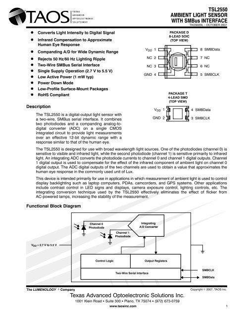
Converts Light Intensity to Digital Signal Infrared Compensation to ApproximateHuman Eye Response Companding A/D for Wide Dynamic Range Rejects 50 Hz/60 Hz Lighting Ripple Two-Wire <strong>SMBus</strong> Serial Interface Single Supply Operation (2.7 V to 5.5 V) Low Active Power (1 mW typ) Power Down Mode Low-Profile Surface-Mount Packages RoHS Compliant<strong>TSL2550</strong><strong>AMBIENT</strong> <strong>LIGHT</strong> <strong>SENSOR</strong><strong>WITH</strong> <strong>SMBus</strong> <strong>INTERFACE</strong>TAOS029L − OCTOBER 2007DescriptionThe <strong>TSL2550</strong> is a digital-output light sensor witha two-wire, <strong>SMBus</strong> serial interface. It combinestwo photodiodes and a companding analog-todigitalconverter (ADC) on a single CMOSintegrated circuit to provide light measurementsover an effective 12-bit dynamic range with aresponse similar to that of the human eye.V DD 1GND 24 SMBData3 SMBCLKThe <strong>TSL2550</strong> is designed for use with broad wavelength light sources. One of the photodiodes (channel 0) issensitive to visible and infrared light, while the second photodiode (channel 1) is sensitive primarily to infraredlight. An integrating ADC converts the photodiode currents to channel 0 and channel 1 digital outputs. Channel1 digital output is used to compensate for the effect of the infrared component of ambient light on channel 0digital output. The ADC digital outputs of the two channels are used to obtain a value that approximates thehuman eye response in the commonly used unit of Lux.This device is intended primarily for use in applications in which measurement of ambient light is used to controldisplay backlighting such as laptop computers, PDAs, camcorders, and GPS systems. Other applicationsinclude contrast control in LED signs and displays, camera exposure control, lighting controls, etc. Theintegrating conversion technique used by the <strong>TSL2550</strong> effectively eliminates the effect of flicker fromAC-powered lamps, increasing the stability of the measurement.Functional Block DiagramV DD 1NC 2NC 3GND 4PACKAGE D8-LEAD SOIC(TOP VIEW)PACKAGE T4-LEAD SMD(TOP VIEW)8 SMBData7 NC6 NC5 SMBCLKChannel 0PhotodiodeChannel 1PhotodiodeIntegratingA/D ConverterV DD = 2.7 V to 5.5 VControl LogicOutput RegistersTwo-Wire Serial InterfaceSMBCLKSMBDataThe LUMENOLOGY CompanyTexas Advanced Optoelectronic Solutions Inc.1001 Klein Road Suite 300 Plano, TX 75074 (972) 673-0759www.taosinc.comCopyright 2007, TAOS Inc.1
<strong>TSL2550</strong><strong>AMBIENT</strong> <strong>LIGHT</strong> <strong>SENSOR</strong><strong>WITH</strong> <strong>SMBus</strong> <strong>INTERFACE</strong>TAOS029L − OCTOBER 2007Terminal FunctionsNAMETERMINALD PKGNO.T PKGNO.TYPEDESCRIPTIONGND 4 2 Power supply ground. All voltages are referenced to GND.SMBCLK 5 3 I <strong>SMBus</strong> serial clock input terminal — clock signal for <strong>SMBus</strong> serial data.SMBData 8 4 I/O <strong>SMBus</strong> serial data I/O terminal — serial data I/O for <strong>SMBus</strong>.V DD 1 1 Supply voltage.Available OptionsDEVICE T A PACKAGE − LEADS PACKAGE DESIGNATOR ORDERING NUMBER<strong>TSL2550</strong> −40°C to 85° SOIC−8 D <strong>TSL2550</strong>D<strong>TSL2550</strong> −40°C to 85° T−4 T <strong>TSL2550</strong>TAbsolute Maximum Ratings over operating free-air temperature range (unless otherwise noted) †Supply voltage, V DD (see Note 1) . . . . . . . . . . . . . . . . . . . . . . . . . . . . . . . . . . . . . . . . . . . . . . . . . . . . . . . . . . . . . 6 VDigital output voltage range, V O . . . . . . . . . . . . . . . . . . . . . . . . . . . . . . . . . . . . . . . . . . . . . . . . . . . . −0.3 V to +6 VDigital output current, I O . . . . . . . . . . . . . . . . . . . . . . . . . . . . . . . . . . . . . . . . . . . . . . . . . . . . . . . . . . . . . . . . . ±10 mA<strong>SMBus</strong> input/output current, I (SMBIN) . . . . . . . . . . . . . . . . . . . . . . . . . . . . . . . . . . . . . . . . . . . . . . . −1 mA to 20 mAOperating free-air temperature range, T A . . . . . . . . . . . . . . . . . . . . . . . . . . . . . . . . . . . . . . . . . . . . −40°C to 85°CStorage temperature range, T stg . . . . . . . . . . . . . . . . . . . . . . . . . . . . . . . . . . . . . . . . . . . . . . . . . . . . −40°C to 85°CESD tolerance, human body model . . . . . . . . . . . . . . . . . . . . . . . . . . . . . . . . . . . . . . . . . . . . . . . . . . . . . . . . 2000 VSolder conditions in accordance with JEDEC J−STD−020A, maximum temperature (see Note 2) . . . 260°C† Stresses beyond those listed under “absolute maximum ratings” may cause permanent damage to the device. These are stress ratings only, andfunctional operation of the device at these or any other conditions beyond those indicated under “recommended operating conditions” is notimplied. Exposure to absolute-maximum-rated conditions for extended periods may affect device reliability.NOTES: 1. All voltage values are with respect to GND.2. Package D only: The device may be hand soldered provided that heat is applied only to the solder pad and no contact is madebetween the tip of the solder iron and the device lead. The maximum time heat should be applied to the device is 5 seconds.Recommended Operating ConditionsMIN MAX UNITSupply voltage, V DD 2.7 5.5 VOperating free-air temperature, T A 0 70 °C<strong>SMBus</strong> input low voltage @ V DD = 3.3 V ± 5%, V IL 0.8 V<strong>SMBus</strong> input high voltage @ V DD = 3.3 V ± 5%, V IH 2.1 V<strong>SMBus</strong> operating frequency, f (SMBCLK) 10 100 kHzCopyright 2007, TAOS Inc.The LUMENOLOGY Company2www.taosinc.com
<strong>TSL2550</strong><strong>AMBIENT</strong> <strong>LIGHT</strong> <strong>SENSOR</strong><strong>WITH</strong> <strong>SMBus</strong> <strong>INTERFACE</strong>TAOS029L − OCTOBER 2007Electrical Characteristics over recommended operating free-air temperature range (unlessotherwise noted)V OLPARAMETER TEST CONDITIONS MIN TYP MAX UNITI O = 50 μA 0.01<strong>SMBus</strong> output low voltageVI O = 4 mA 0.4I DDSupply currentActive, VSMBCLK and VSMDATA = V DD,V DD = 3.3 V ± 5%Power down, VSMBCLK and VSMDATA =V DD, V DD = 3.3 V ± 5%0.35 0.6 mA10 μAI IH High level input current VI = V DD 5 μAI IL Low level input current VI = 0 −5 μAOperating Characteristics, V DD = 3.3 V, T A = 25C (unless otherwise noted) (see Notes 2, 3, 4)R eR vPARAMETER TEST CONDITIONS CHANNEL MIN TYP MAX UNITADC count value, standard modeADC count value, extended modeE e = 0Ch0 1Ch1 1λ p = 640 nmCh0 639 799 959E e = 72 μW/cm 2 Ch1 85λ p = 940 nmCh0 511 799 1039E e = 140 μW/cm 2 Ch1 703E e = 0Ch0 1Ch1 1λ p = 640 nmCh0 155E e = 72 μW/cm 2 Ch1 16λ p = 940 nmCh0 155E e = 140 μW/cm 2 Ch1 139ADC count value ratio: Ch1/Ch0,λ p = 640 nm, E e = 72 μW/cm 2 0.070 0.106 0.175standard mode λ p = 940 nm, E e = 140 μW/cm 2 0.70 0.88 1.20Irradiance responsivity, standard modeIlluminance responsivity, standard modecountscountsλ p = 640 nmCh0 11.1E e = 72 μW/cm 2 Ch1 1.2 counts/(μW/λ p = 940 nmCh0 5.7cm 2 )E e = 140 μW/cm 2 Ch1 5Fluorescent light source: 300 LuxIncandescent light source: 50 LuxCh0 2.8Ch1 0.23 counts/Ch0 19luxCh1 13(Sensor Lux) / (actual Lux), standard mode Fluorescent light source: 300 Lux 0.65 1 1.35(Note 5) Incandescent light source: 50 Lux 0.5 1 1.5NOTES: 3. Optical measurements are made using small-angle incident radiation from light-emitting diode optical sources. Visible 640 nm LEDsand infrared 940 nm LEDs are used for final product testing for compatibility with high volume production.4. The 640 nm irradiance E e is supplied by an AlInGaP light-emitting diode with the following characteristics: peak wavelengthλp = 640 nm and spectral halfwidth Δλ½ = 17 nm.5. The 940 nm irradiance E e is supplied by a GaAs light-emitting diode with the following characteristics: peak wavelengthλp = 940 nm and spectral halfwidth Δλ½ = 40 nm.6. The sensor Lux is calculated using the empirical formula shown on p. 11 of this data sheet based on measured Ch0 and Ch1 ADCcount values for the light source specified. Actual Lux is obtained with a commercial luxmeter. The range of the (sensor Lux) / (actualLux) ratio is estimated based on the variation of the 640 nm and 940 nm optical parameters. Devices are not 100% tested withfluorescent or incandescent light sources.The LUMENOLOGY CompanyCopyright 2007, TAOS Inc.www.taosinc.com3
<strong>TSL2550</strong><strong>AMBIENT</strong> <strong>LIGHT</strong> <strong>SENSOR</strong><strong>WITH</strong> <strong>SMBus</strong> <strong>INTERFACE</strong>TAOS029L − OCTOBER 2007AC Electrical Characteristics, V DD = 3.3 V, T A = 25C (unless otherwise noted)PARAMETER TEST CONDITIONS MIN TYP MAX UNITt (CONV) Conversion time, per channel, standard mode 400 mst (CONV) Conversion time, per channel, extended mode 80 msf (SMBCLK) Clock frequency 100 kHzt (BUF) Bus free time between start and stop condition 4.7 μst (HDSTA)Hold time after (repeated) start condition. Afterthis period, the first clock is generated.4 μst (SUSTA) Repeated start condition setup time 4.7 μst (SUSTO) Stop condition setup time 4 μst (HDDAT) Data hold time 300 nst (SUDAT) Data setup time 250 nst (LOW) SMBCLK clock low period 4.7 μst (HIGH) SMBCLK clock high period 4 μst (TIMEOUT) Detect clock/data low timeout 25 35 mst F Clock/data fall time 300 nst R Clock/data rise time 1000 nsC i Input pin capacitance 10 pFCopyright 2007, TAOS Inc.The LUMENOLOGY Company4www.taosinc.com
PARAMETER MEASUREMENT INFORMATION<strong>TSL2550</strong><strong>AMBIENT</strong> <strong>LIGHT</strong> <strong>SENSOR</strong><strong>WITH</strong> <strong>SMBus</strong> <strong>INTERFACE</strong>TAOS029L − OCTOBER 2007t (LOW)t (R)t (F)SMBCLKV IHV ILt (HDSTA)t (HIGH)t (SUSTA)t (BUF)t (HDDAT)t (SUDAT)t (SUSTO)SMBDATAV IHV ILPStopConditionSStartConditionStartSStopPt (LOWMEXT)t (LOWSEXT)SMBCLK ACKt (LOWMEXT)t (LOWMEXT)SMBCLK ACKSMBCLKSMBDATAFigure 1. <strong>SMBus</strong> Timing Diagrams1 9 1 9SMBCLKSMBDATAA6A5A4A3A2A1A0R/WD7D6D5D4D3D2D1D0Start byMasterACK by<strong>TSL2550</strong>ACK by<strong>TSL2550</strong>Stop byMasterFrame 1 <strong>SMBus</strong> Slave Address ByteFrame 2 Command ByteFigure 2. <strong>SMBus</strong> Timing Diagram for Send Byte Format1 9 1 9SMBCLKSMBDATAA6A5A4A3A2A1A0R/WD7D6D5D4D3D2D1D0Start byMasterACK by<strong>TSL2550</strong>NACK byMasterStop byMasterFrame 1 <strong>SMBus</strong> Slave Address ByteFrame 2 Data Byte From <strong>TSL2550</strong>Figure 3. <strong>SMBus</strong> Timing Diagram for Receive Byte FormatThe LUMENOLOGY CompanyCopyright 2007, TAOS Inc.www.taosinc.com5
<strong>TSL2550</strong><strong>AMBIENT</strong> <strong>LIGHT</strong> <strong>SENSOR</strong><strong>WITH</strong> <strong>SMBus</strong> <strong>INTERFACE</strong>TAOS029L − OCTOBER 2007TYPICAL CHARACTERISTICSSPECTRAL RESPONSIVITYNORMALIZED ADC OUTPUTvs.SUPPLY VOLTAGE11.81.6Relative Responsivity0.80.60.40.2Channel 1PhotodiodeChannel 0PhotodiodeNormalized ADC Output1.41.210.80.60.40.20400500 600 700 800 900 1000 1100λ − Wavelength − nmFigure 402.5 3 3.5 4 4.5 5 5.5 6V DD − Supply Voltage − VFigure 5Copyright 2007, TAOS Inc.The LUMENOLOGY Company6www.taosinc.com
<strong>TSL2550</strong><strong>AMBIENT</strong> <strong>LIGHT</strong> <strong>SENSOR</strong><strong>WITH</strong> <strong>SMBus</strong> <strong>INTERFACE</strong>TAOS029L − OCTOBER 2007PRINCIPLES OF OPERATIONAnalog-to-Digital ConverterThe <strong>TSL2550</strong> contains an integrating analog-to-digital converter (ADC) that integrates a photodiode current.First it integrates channel 0 photodiode current and then it integrates channel 1 photodiode current. At the endof the conversion cycle for each channel, the conversion result is transferred to the appropriate channel 0 orchannel 1 ADC register. The transfer is double-buffered to ensure that invalid data is not read during the transfer.After the data is transferred, the <strong>TSL2550</strong> automatically begins the next conversion cycle. A VALID bit is usedto indicate that data has been written to the ADC register after ADC is enabled.Interface to the ADC and control of other device functions is accomplished using the standard 2-wire SystemManagement Bus (<strong>SMBus</strong>) interface. Both versions 1.1 and 2.0 of the <strong>SMBus</strong> are supported.The ADC has two operating modes: standard and extended. In standard mode, the integration time is 400 mSfor each channel or 800 mS for both channel 0 and channel 1. Extended mode shortens the integration timeby a factor of five with a corresponding decrease in responsivity of 5×. The extended range allows the deviceto operate at higher light levels, extending the overall dynamic range by a factor of five.Digital InterfaceThe <strong>TSL2550</strong> contains an 8-bit command register that can be written and read via the <strong>SMBus</strong>. The commandregister controls the overall operation of the device. There are two read-only registers that contain the latestconverted value of each of the two ADC channels. The <strong>SMBus</strong> slave address is hardwired internally as 0111001(MSB to LSB, A6 to A0).Both the send byte protocol and the receive byte protocol are implemented in the <strong>TSL2550</strong>. The send byteprotocol allows single bytes of data to be written to the device (see Figure 6). The written byte is called theCOMMAND byte. The receive byte protocol allows single bytes of data to be read from the device (see Figure7). The receive data can be either the previously written COMMAND byte or the data from one of the ADCchannels. In Figure 6 and Figure 7, the clear area represents data sent by the host and the shaded arearepresents data returned by the ambient light sensor or slave device.1S7Slave Address1 1 8 1 1WRAData ByteAPS = Start Condition P = Stop Condition Shaded = Slave TransmissionFigure 6. Send Byte Protocol1S7Slave Address1 1 8 1 1RDAData ByteAPS = Start Condition P = Stop Condition Shaded = Slave TransmissionFigure 7. Receive Byte ProtocolThe LUMENOLOGY CompanyCopyright 2007, TAOS Inc.www.taosinc.com7
<strong>TSL2550</strong><strong>AMBIENT</strong> <strong>LIGHT</strong> <strong>SENSOR</strong><strong>WITH</strong> <strong>SMBus</strong> <strong>INTERFACE</strong>TAOS029L − OCTOBER 2007Command RegisterThe command register is used primarily to:Select which ADC register will be read during a read cycleSwitch the dynamic range of the device between standard and extended range modes Power the device up for operation or power it down for minimum power consumptionTable 1 shows the six primary commands used to control the <strong>TSL2550</strong>.Table 1. Command SummaryCOMMANDFUNCTION0x00hPower-down state0x03hPower-up state/Read command register0x1DhWrite command to assert extended range mode0x18hWrite command to reset or return to standard range mode0x43h Read ADC channel 00x83h Read ADC channel 1The content of the command register defaults to 0x00h when power is applied to the device, placing the deviceinto the power-down mode.Once the <strong>TSL2550</strong> is set to the standard range mode (0x18h) or the extended range mode (0x1Dh), the deviceremains in that mode until it is powered down or the mode is changed via the command register.The 0x03h command has two purposes: It is used to power up the device and can also be used to check thatthe device is communicating properly. The value returned during a read cycle should be 0x03h.ADC RegisterThe <strong>TSL2550</strong> contains two ADC registers (channel 0 and channel 1). Each ADC register contains twocomponent fields that are used to determine the logarithmic ADC count value: CHORD bits and STEP bits. TheCHORD bits correspond to the most significant portion of the ADC value and specifies a segment of thepiece-wise linear approximation. The STEP bits correspond to the least significant portion of the ADC countvalue and specifies a linear value within a segment. CHORD and STEP bits all equal to 0 corresponds to acondition in which the light level is below the detection limit of the sensor. CHORD and STEP bits all equal to1 corresponds to an overflow condition.Each of the two ADC value registers contain seven data bits and a valid bit as described in Table 2.Table 2. ADC Register Data FormatVALID CHORD BITS STEP BITSB7 B6 B5 B4 B3 B2 B1 B0VALID C2 C1 C0 S3 S2 S1 S0FIELD BITS DESCRIPTIONVALID 7ADC channel data is valid. One indicates that the ADC has written data into thechannel data register, since ADCEN was asserted in the COMMAND register.CHORD 6 to 4 CHORD number.STEP 3 to 0 STEP number.Copyright 2007, TAOS Inc.The LUMENOLOGY Company8www.taosinc.com
<strong>TSL2550</strong><strong>AMBIENT</strong> <strong>LIGHT</strong> <strong>SENSOR</strong><strong>WITH</strong> <strong>SMBus</strong> <strong>INTERFACE</strong>TAOS029L − OCTOBER 2007The specific ADC value register read depends on the last read command written to the command register, asdescribed above and in the Operation section, below.The MSB of the ADC register (VALID bit B7) is used to indicate that data has been written to the ADC registerafter the device is powered up as described in Command Register section.Bits 6 through 0 contain the 7-bit code representing the ADC count value, which is proportional to aphotodetector current. In this code, the ADC count value is represented by a piece-wise linear approximationto a log function. The transfer function is broken into 8 chords of 16 steps each. (This code is very similar to μ-lawcode used in audio compression — it differs in that it does not have a sign bit and it is not inverted.) Table 3 showsthe relationship between the CHORD and STEP bits and the CHORD and STEP numbers and values. Theseare used to calculate the ADC count value.Table 3. CHORD and STEP Numbers and Values vs Register BitsCHORDBITSB6, B5, B4C, CHORDNUMBERCHORDVALUE(Note A)STEPVALUE(Note B)STEPBITSB3, B2, B1, B0S, STEPNUMBER000 0 0 1 0000 0001 1 16 2 0001 1010 2 49 4 0010 2011 3 115 8 0011 3100 4 247 16 0100 4101 5 511 32 0101 5110 6 1039 64 0110 6111 7 2095 128 0111 71000 81001 91010 101011 111100 121101 131110 141111 15NOTES: A. CHORD VALUE = INT (16.5 × ((2 C ) − 1))B. STEP VALUE = 2 CThe ADC count value is obtained by adding the CHORD VALUE and the product of the STEP NUMBER andSTEP VALUE (which depends on CHORD NUMBER).ADC Count Value ((Chord Value) (Step Value) (Step Number))The ADC count value can also be expressed as a formula:ADC Count Value (INT (16.5 ((2 C 1))) (S (2 C ))where:C is the CHORD NUMBER (0 to 7)S is the STEP NUMBER (0 to 15)as defined in Table 3.The LUMENOLOGY CompanyCopyright 2007, TAOS Inc.www.taosinc.com9
<strong>TSL2550</strong><strong>AMBIENT</strong> <strong>LIGHT</strong> <strong>SENSOR</strong><strong>WITH</strong> <strong>SMBus</strong> <strong>INTERFACE</strong>TAOS029L − OCTOBER 2007OperationAfter applying VDD, the device will initially be in the power down state. To operate the device, issue an <strong>SMBus</strong>Send Byte protocol with the device address and the appropriate command byte to read ADC channel 0 or ADCchannel 1 (see Table 1). To obtain the conversion result, issue an <strong>SMBus</strong> Receive Byte protocol with the deviceaddress. The data byte received will correspond to the value in the ADC register (0 or 1) specified by the previouscommand. If a conversion has not been completed since power up (either through V DD or power up command),the valid bit will be 0, and the data will not be valid. If there is a valid conversion result available, the valid bitwill be set (1), and the remaining 7 bits will represent valid data from the previously selected ADC register. Datamay be read repeatedly from the currently selected ADC register, and although it will remain valid, the ADCregister will not be updated until a new conversion completes for that channel (800 ms total since there are twoserial 400 ms per channel conversion times in standard mode). Note also that the command register itself maybe read, as a check to be sure that the device is communicating properly.To power down the device for reduced power consumption, issue an <strong>SMBus</strong> Send Byte protocol with the deviceaddress followed by 0 as indicated in Table 1.Copyright 2007, TAOS Inc.The LUMENOLOGY Company10www.taosinc.com
<strong>TSL2550</strong><strong>AMBIENT</strong> <strong>LIGHT</strong> <strong>SENSOR</strong><strong>WITH</strong> <strong>SMBus</strong> <strong>INTERFACE</strong>TAOS029L − OCTOBER 2007APPLICATION INFORMATIONThe <strong>TSL2550</strong> is intended for use in ambient light detection applications, such as display backlight control, whereadjustments are made to display brightness or contrast based on the brightness of the ambient light, asperceived by the human eye. Conventional silicon detectors respond strongly to infrared light, which the humaneye does not see. This can lead to significant error when the infrared content of the ambient light is high, suchas with incandescent lighting, due to the difference between the silicon detector response and the brightnessperceived by the human eye.This problem is overcome in the <strong>TSL2550</strong> through the use of two photodiodes. One of the photodiodes(channel 0) is sensitive to both visible and infrared light, while the second photodiode (channel 1) is sensitiveprimarily to infrared light. An integrating ADC converts the photodiode currents to channel 0 and channel 1 digitaloutputs. Channel 1 digital output is used to compensate for the effect of the infrared component of light on thechannel 0 digital output. The ADC digital outputs from the two channels are used in a formula to obtain a valuethat approximates the human eye response in the commonly used Illuminance unit of Lux. For standard mode:where:Light Level (lux) (Ch0 Ch1) 0.39 e (0.181R2 )R = Ch1 Counts / (Ch0 Counts − Ch1 Counts)The formula above was obtained by optical testing with fluorescent and incandescent light sources. The lightlevel calculated from the formula will be slightly higher than the actual light level for sunlight and will be slightlylower than the actual light level for composite fluorescent and incandescent light sources.NOTE:Please see TAOS application notes for additional information, including implementing a displaybrightness control system with the <strong>TSL2550</strong>, and for a simple implementation of the equation shownabove suitable for use in embedded microcontrollers.Table 4 contains a summary of the typical sensor outputs for several common light sources.<strong>LIGHT</strong> SOURCETable 4. Sensor Output Summary (Standard Mode)ILLUMINANCE(LUX)CHANNEL 0(COUNTS)CHANNEL 1(COUNTS)RATIO:CH1/CH0LUX per CH0COUNTFluorescent 297 831 68 0.082 0.36Daylight (shade) 201 895 343 0.383 0.22Incandescent 42 959 671 0.7 0.04Light from 50 or 60 Hz sources, and especially fluorescent lighting, has a high harmonic content. Since the<strong>TSL2550</strong> integrates the ambient light over an approximately 400 millisecond interval (per channel), this lightripple is typically reduced to less than ¼ LSB.Power Supply DecouplingThe power supply lines must be decoupled with a 0.1 μF capacitor placed as close to the device package aspossible. The bypass capacitor should have low effective series resistance (ESR) and effective seriesinductance (ESI), such as the common ceramic types, which provide a low impedance path to ground at highfrequencies to handle transient currents caused by internal logic switching.The LUMENOLOGY CompanyCopyright 2007, TAOS Inc.www.taosinc.com11
<strong>TSL2550</strong><strong>AMBIENT</strong> <strong>LIGHT</strong> <strong>SENSOR</strong><strong>WITH</strong> <strong>SMBus</strong> <strong>INTERFACE</strong>TAOS029L − OCTOBER 2007APPLICATION INFORMATIONPCB Pad LayoutSuggested PCB pad layout guidelines for the D package and T package are shown in Figure 8 and Figure 9.4.656.901.270.502.25NOTES: A. All linear dimensions are in millimeters.B. This drawing is subject to change without notice.Figure 8. Suggested D Package PCB Layout2.901.501.000.90NOTES: A. All linear dimensions are in millimeters.B. This drawing is subject to change without notice.Figure 9. Suggested T Package PCB LayoutCopyright 2007, TAOS Inc.The LUMENOLOGY Company12www.taosinc.com
<strong>TSL2550</strong><strong>AMBIENT</strong> <strong>LIGHT</strong> <strong>SENSOR</strong><strong>WITH</strong> <strong>SMBus</strong> <strong>INTERFACE</strong>TAOS029L − OCTOBER 2007MECHANICAL DATAPACKAGE DPlastic Small-OutlineTOP VIEWBOTTOM VIEWPIN 1PIN 16 1.27SIDE VIEWNOTE B 2.8 TYPCLEAR WINDOW8 0.5100.330END VIEW5.004.800.500.25450.88 TYP TOP OF<strong>SENSOR</strong> DIE5.3MAXA1.751.35DETAIL A4.003.806.205.800.250.19Pb1.270.410.250.10NOTES: A. All linear dimensions are in millimeters.B. The center of the 1234 μm by 282 μm photo-active area is typically located in the center of the package in the long dimension and269 μm off center in the short dimension.C. Package is molded with an electrically nonconductive clear plastic compound having an index of refraction of 1.55.D. This drawing is subject to change without notice.Figure 10. Package D — Plastic Small Outline IC Packaging ConfigurationThe LUMENOLOGY CompanyCopyright 2007, TAOS Inc.www.taosinc.com13
<strong>TSL2550</strong><strong>AMBIENT</strong> <strong>LIGHT</strong> <strong>SENSOR</strong><strong>WITH</strong> <strong>SMBus</strong> <strong>INTERFACE</strong>TAOS029L − OCTOBER 2007MECHANICAL DATAPACKAGE TFour-Lead Surface Mount DeviceTOP VIEWPHOTODIODE ACTIVE AREA LOCATIONPIN 11.50PIN 40.671.460.281.230.55SIDE VIEW0.501.350.353.102 70.10DETAIL A: TYPICAL PACKAGE TERMINAL0.90BOTTOM VIEWA0.780.78R 0.252.60PIN 1PIN 43.80PbNOTES: A. All linear dimensions are in millimeters.B. Terminal finish is gold.C. Dimension tolerance is ± 0.15 mm.D. This drawing is subject to change without notice.Figure 11. Package T — Four-Lead Surface Mount Device Packaging ConfigurationCopyright 2007, TAOS Inc.The LUMENOLOGY Company14www.taosinc.com
<strong>TSL2550</strong><strong>AMBIENT</strong> <strong>LIGHT</strong> <strong>SENSOR</strong><strong>WITH</strong> <strong>SMBus</strong> <strong>INTERFACE</strong>TAOS029L − OCTOBER 2007MECHANICAL DATASIDE VIEWK o2.11 0.10 [0.083 0.004]0.292 0.013[0.0115 0.0005]TOP VIEWEND VIEW 1.508 0.1[0.315 0.004]4 0.1[0.157 0.004]2 0.05[0.079 0.002]1.75 0.10[0.069 0.004]B5.50 0.05[0.217 0.002]12 + 0.3 − 0.1[0.472 + 0.12 − 0.004]AABDETAIL ADETAIL BA o6.45 0.10[0.254 0.004]B o5.13 0.10[0.202 0.004]NOTES: A. All linear dimensions are in millimeters [inches].B. The dimensions on this drawing are for illustrative purposes only. Dimensions of an actual carrier may vary slightly.C. Symbols on drawing A o , B o , and K o are defined in ANSI EIA Standard 481−B 2001.D. Each reel is 178 millimeters in diameter and contains 1000 parts.E. TAOS packaging tape and reel conform to the requirements of EIA Standard 481−B.F. In accordance with EIA standard, device pin 1 is located next to the sprocket holes in the tape.G. This drawing is subject to change without notice.Figure 12. Package D Carrier TapeThe LUMENOLOGY CompanyCopyright 2007, TAOS Inc.www.taosinc.com15
<strong>TSL2550</strong><strong>AMBIENT</strong> <strong>LIGHT</strong> <strong>SENSOR</strong><strong>WITH</strong> <strong>SMBus</strong> <strong>INTERFACE</strong>TAOS029L − OCTOBER 2007MECHANICAL DATA0.30 0.050 2.10SIDE VIEW1.75 0.1008 TypB 1.504 0.1002 0.100END VIEWTOP VIEW12 0.1005.50 0.100 1.50R 0.20 TYPBAADETAIL ADETAIL B2.90 0.100 A o3.09 MAXR 0.20 TYPR 0.20 TYP4.29 MAX4.10 0.100 B o1.80 K oNOTES: A. All linear dimensions are in millimeters.B. The dimensions on this drawing are for illustrative purposes only. Dimensions of an actual carrier may vary slightly.C. Symbols on drawing A o , B o , and K o are defined in ANSI EIA Standard 481−B 2001.D. Each reel is 178 millimeters in diameter and contains 1000 parts.E. TAOS packaging tape and reel conform to the requirements of EIA Standard 481−B.F. In accordance with EIA standard, device pin 1 is located next to the sprocket holes in the tape.G. This drawing is subject to change without notice.Figure 13. Package T Carrier TapeCopyright 2007, TAOS Inc.The LUMENOLOGY Company16www.taosinc.com
<strong>TSL2550</strong><strong>AMBIENT</strong> <strong>LIGHT</strong> <strong>SENSOR</strong><strong>WITH</strong> <strong>SMBus</strong> <strong>INTERFACE</strong>TAOS029L − OCTOBER 2007MANUFACTURING INFORMATIONThe D and T packages have been tested and have demonstrated an ability to be reflow soldered to a PCBsubstrate. The process, equipment, and materials used in these test are detailed below.The solder reflow profile describes the expected maximum heat exposure of components during the solderreflow process of product on a PCB. Temperature is measured on top of component. The components shouldbe limited to a maximum of three passes through this solder reflow profile.Table 5. <strong>TSL2550</strong> Solder Reflow ProfilePARAMETER REFERENCE <strong>TSL2550</strong>D/<strong>TSL2550</strong>TAverage temperature gradient in preheating2.5°C/secSoak time t soak 2 to 3 minutesTime above 217°C t 1 Max 60 secTime above 230°C t 2 Max 50 secTime above T peak −10°C t 3 Max 10 secPeak temperature in reflow T peak 260° C (−0°C/+5°C)Temperature gradient in coolingMax −5°C/secT peakT 3Not to scale — for reference onlyT 2T 1Temperature (C)Time (sec)t 3t 2t soakt 1Figure 14. <strong>TSL2550</strong>D/<strong>TSL2550</strong>T Solder Reflow Profile GraphThe LUMENOLOGY CompanyCopyright 2007, TAOS Inc.www.taosinc.com17
<strong>TSL2550</strong><strong>AMBIENT</strong> <strong>LIGHT</strong> <strong>SENSOR</strong><strong>WITH</strong> <strong>SMBus</strong> <strong>INTERFACE</strong>TAOS029L − OCTOBER 2007MANUFACTURING INFORMATIONMoisture SensitivityOptical characteristics of the device can be adversely affected during the soldering process by the release andvaporization of moisture that has been previously absorbed into the package molding compound.Package DTo ensure the package molding compound contains the smallest amount of absorbed moisture possible, alldevices shipped in carrier tape have been pre-baked and shipped in a sealed moisture-barrier bag. No furtheraction is necessary if these devices are processed through solder reflow within 24 hours of the seal being brokenon the moisture-barrier bag.However, for all devices shipped in tubes or if the seal on the moisture barrier bag has been broken for 24 hoursor longer, it is recommended that the following procedures be used to ensure the package molding compoundcontains the smallest amount of absorbed moisture possible.For devices shipped in tubes:1. Remove devices from tubes2. Bake devices for 4 hours, at 90°C3. After cooling, load devices back into tubes4. Perform solder reflow within 24 hours after bakeBake only a quantity of devices that can be processed through solder reflow in 24 hours. Devices can bere-baked for 4 hours, at 90°C for a cumulative total of 12 hours (3 bakes for 4 hours at 90°C).For devices shipped in carrier tape:1. Bake devices for 4 hours, at 90°C in the tape2. Perform solder reflow within 24 hours after bakeBake only a quantity of devices that can be processed through solder reflow in 24 hours. Devices can bere−baked for 4 hours in tape, at 90°C for a cumulative total of 12 hours (3 bakes for 4 hours at 90°C).Package TTo ensure the package molding compound contains the smallest amount of absorbed moisture possible, eachdevice is dry-baked prior to being packed for shipping. Devices are packed in a sealed aluminized envelopewith silica gel to protect them from ambient moisture during shipping, handling, and storage before use.The T package has been assigned a moisture sensitivity level of MSL 3 and the devices should be stored underthe following conditions:Temperature Range 5°C to 50°CRelative Humidity 60% maximumTotal Time6 months from the date code on the aluminized envelope — if unopenedOpened Time 168 hours or fewerRebaking will be required if the devices have been stored unopened for more than 6 months or if the aluminizedenvelope has been open for more than 168 hours. If rebaking is required, it should be done at 90°C for 4 hours.Copyright 2007, TAOS Inc.The LUMENOLOGY Company18www.taosinc.com
<strong>TSL2550</strong><strong>AMBIENT</strong> <strong>LIGHT</strong> <strong>SENSOR</strong><strong>WITH</strong> <strong>SMBus</strong> <strong>INTERFACE</strong>TAOS029L − OCTOBER 2007PRODUCTION DATA — information in this document is current at publication date. Products conform tospecifications in accordance with the terms of Texas Advanced Optoelectronic Solutions, Inc. standardwarranty. Production processing does not necessarily include testing of all parameters.LEAD-FREE (Pb-FREE) and GREEN STATEMENTPb-Free (RoHS) TAOS’ terms Lead-Free or Pb-Free mean semiconductor products that are compatible with the currentRoHS requirements for all 6 substances, including the requirement that lead not exceed 0.1% by weight in homogeneousmaterials. Where designed to be soldered at high temperatures, TAOS Pb-Free products are suitable for use in specifiedlead-free processes.Green (RoHS & no Sb/Br) TAOS defines Green to mean Pb-Free (RoHS compatible), and free of Bromine (Br) andAntimony (Sb) based flame retardants (Br or Sb do not exceed 0.1% by weight in homogeneous material).Important Information and Disclaimer The information provided in this statement represents TAOS’ knowledge andbelief as of the date that it is provided. TAOS bases its knowledge and belief on information provided by third parties,and makes no representation or warranty as to the accuracy of such information. Efforts are underway to better integrateinformation from third parties. TAOS has taken and continues to take reasonable steps to provide representativeand accurate information but may not have conducted destructive testing or chemical analysis on incoming materials andchemicals. TAOS and TAOS suppliers consider certain information to be proprietary, and thus CAS numbers and otherlimited information may not be available for release.NOTICETexas Advanced Optoelectronic Solutions, Inc. (TAOS) reserves the right to make changes to the products contained in thisdocument to improve performance or for any other purpose, or to discontinue them without notice. Customers are advisedto contact TAOS to obtain the latest product information before placing orders or designing TAOS products into systems.TAOS assumes no responsibility for the use of any products or circuits described in this document or customer productdesign, conveys no license, either expressed or implied, under any patent or other right, and makes no representation thatthe circuits are free of patent infringement. TAOS further makes no claim as to the suitability of its products for any particularpurpose, nor does TAOS assume any liability arising out of the use of any product or circuit, and specifically disclaims anyand all liability, including without limitation consequential or incidental damages.TEXAS ADVANCED OPTOELECTRONIC SOLUTIONS, INC. PRODUCTS ARE NOT DESIGNED OR INTENDED FORUSE IN CRITICAL APPLICATIONS IN WHICH THE FAILURE OR MALFUNCTION OF THE TAOS PRODUCT MAYRESULT IN PERSONAL INJURY OR DEATH. USE OF TAOS PRODUCTS IN LIFE SUPPORT SYSTEMS IS EXPRESSLYUNAUTHORIZED AND ANY SUCH USE BY A CUSTOMER IS COMPLETELY AT THE CUSTOMER’S RISK.LUMENOLOGY, TAOS, the TAOS logo, and Texas Advanced Optoelectronic Solutions are registered trademarks of Texas AdvancedOptoelectronic Solutions Incorporated.The LUMENOLOGY CompanyCopyright 2007, TAOS Inc.www.taosinc.com19
<strong>TSL2550</strong><strong>AMBIENT</strong> <strong>LIGHT</strong> <strong>SENSOR</strong><strong>WITH</strong> <strong>SMBus</strong> <strong>INTERFACE</strong>TAOS029L − OCTOBER 2007Copyright 2007, TAOS Inc.The LUMENOLOGY Company20www.taosinc.com