BPY 62 NPN-Silizium-Fototransistor Silicon NPN Phototransistor ...
BPY 62 NPN-Silizium-Fototransistor Silicon NPN Phototransistor ...
BPY 62 NPN-Silizium-Fototransistor Silicon NPN Phototransistor ...

Create successful ePaper yourself
Turn your PDF publications into a flip-book with our unique Google optimized e-Paper software.
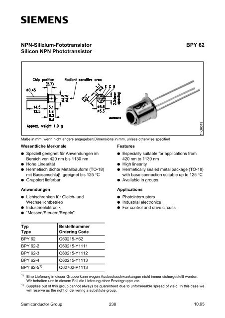
<strong>BPY</strong> <strong>62</strong><strong>NPN</strong>-<strong>Silizium</strong>-<strong>Fototransistor</strong><strong>Silicon</strong> <strong>NPN</strong> <strong>Phototransistor</strong><strong>BPY</strong> <strong>62</strong>Maße in mm, wenn nicht anders angegeben/Dimensions in mm, unless otherwise specifiedWesentliche MerkmaleFeatures● Speziell geeignet für Anwendungen imBereich von 420 nm bis 1130 nm● Hohe Linearität● Hermetisch dichte Metallbauform (TO-18)mit Basisanschluβ, geeignet bis 125 °C● Gruppiert lieferbarfmof6019● Especially suitable for applications from420 nm to 1130 nm● High linearity● Hermetically sealed metal package (TO-18)with base connection suitable up to 125 °C● Available in groupsAnwendungen● Lichtschranken für Gleich- undWechsellichtbetrieb● Industrieelektronik● “Messen/Steuern/Regeln”Applications● Photointerrupters● Industrial electronics● For control and drive circuitsTypType<strong>BPY</strong> <strong>62</strong><strong>BPY</strong> <strong>62</strong>-2<strong>BPY</strong> <strong>62</strong>-3<strong>BPY</strong> <strong>62</strong>-4<strong>BPY</strong> <strong>62</strong>-5 1)BestellnummerOrdering CodeQ60215-Y<strong>62</strong>Q60215-Y1111Q60215-Y1112Q60215-Y1113Q<strong>62</strong>702-P11131) Eine Lieferung in dieser Gruppe kann wegen Ausbeuteschwankungen nicht immer sichergestellt werden.Wir behalten uns in diesem Fall die Lieferung einer Ersatzgruppe vor.1) Supplies out of this group cannot always be guaranteed due to unforseeable spread of yield. In this case wewill reserve us the right of delivering a substitute group.Semiconductor Group 23810.95
<strong>BPY</strong> <strong>62</strong>GrenzwerteMaximum RatingsBezeichnungDescriptionBetriebs- und LagertemperaturOperating and storage temperature rangeLöttemperatur bei TauchlötungLötstelle ≥ 2 mm vom Gehäuse,Lötzeit t ≤ 5 sDip soldering temperature ≥ 2 mm distancefrom case bottom, soldering time t ≤ 5 sLöttemperatur bei KolbenlötungLötstelle ≥ 2 mm vom Gehäuse,Lötzeit t ≤ 3 sIron soldering temperature ≥ 2 mm distancefrom case bottom, soldering time t ≤ 3 sKollektor-EmitterspannungCollector-emitter voltageKollektorstromCollector currentKollektorspitzenstrom, τ < 10 µsCollector surge currentEmitter-BasisspannungEmitter-base voltageVerlustleistung, T A = 25 °CTotal power dissipationWärmewiderstandThermal resistanceSymbolSymbolWertValueT op ; T stg – 55 ... + 125 °CT S 260 °CT S 300 °CV CE 50 VI C 100 mAI CS 200 mAV EB 7 VEinheitUnitP tot 200 mWR thJA 500 K/WSemiconductor Group 239
<strong>BPY</strong> <strong>62</strong>Die <strong>Fototransistor</strong>en werden nach ihrer Fotoempfindlichkeit gruppiert und mit arabischenZiffern gekennzeichnet.The phototransistors are grouped according to their spectral sensitivity and distinguishedby arabian figures.BezeichnungDescriptionSymbolSymbolWertValueEinheitUnit-2 -3 -4 -5Fotostrom, λ = 950 nmPhotocurrentE e = 0.5 mW/cm 2 , V CE = 5 VE v = 1000 Ix, Normlicht/standard lightA,V CE = 5 VI PCE 0.5 ... 1.0I PCE 3.00.8 ... 1.64.61.25 ... 2.57.2≥ 2.011.4mAmAAnstiegszeit/AbfallzeitRise and fall timeI C = 1 mA, V CC = 5 V, R L = 1 kΩt r , t f 5 7 9 12 µsKollektor-Emitter-SättigungsspannungCollector-emitter saturation voltageI C = I 1) PCEmin × 0.3,E e = 0.5 mW/cm 2 V CEsat 150 150 160 180 mVStromverstärkungCurrent gainE e = 0.5 mW/cm 2 , V CE = 5 VI PCE 170 270 420 670I PCB1)1)I PCEmin ist der minimale Fotostrom der jeweiligen GruppeI PCEmin is the min. photocurrent of the specified groupSemiconductor Group 241
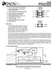
<strong>BPY</strong> <strong>62</strong>Relative spectral sensitivityS rel = f (λ)PhotocurrentI PCE = f (E e ), V CE = 5 VTotal power dissipationP tot = f (T A )Output characteristicsI C = f (V CE ), I B = ParameterOutput characteristicsI C = f (V CE ), I B = ParameterDark currentI CEO = f (V CE ), E = 0PhotocurrentI PCE /I PCE25o= f (T A ), V CE = 5 VDark currentI CEO /I CEO25 o = f (T A ), V CE = 25 V, E = 0Collector-emitter capacitanceC CE = f (V CE ), f = 1 MHz, E = 0Semiconductor Group 242
<strong>BPY</strong> <strong>62</strong>Collector-base capacitanceC CB = f (V CB ), f = 1 MHz, E = 0Emitter-base capacitanceC EB = f (V EB ), f = 1 MHz, E = 0Directional characteristics S rel = f (ϕ)Semiconductor Group 243