Resolution Limits of CA Resists – Low activation Energy ... - IDEMA
Resolution Limits of CA Resists – Low activation Energy ... - IDEMA
Resolution Limits of CA Resists – Low activation Energy ... - IDEMA
- No tags were found...
You also want an ePaper? Increase the reach of your titles
YUMPU automatically turns print PDFs into web optimized ePapers that Google loves.
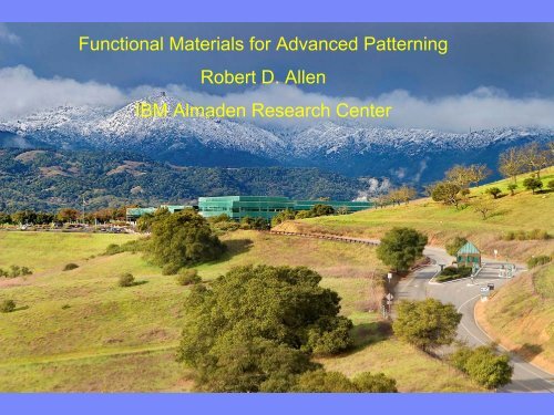
Functional Materials for Advanced PatterningRobert D. AllenBusiness Unit or Product NameIBM Almaden Research Center© 2003 IBM Corporation
IBM Research<strong>Resists</strong>/Materials for Advanced Patterning• Trends in Lithography and Materials Implications• Chemical Amplification----unlocking the potential <strong>of</strong> lithography throughmaterials and chemistry• 193nm Lithography---materials challenges, amazing extendibility• Immersion• Extending Immersion (time permitting)<strong>–</strong> High Index<strong>–</strong> Double Patterning• Post-immersion lithography candidates<strong>–</strong> EUV<strong>–</strong> EB<strong>–</strong> Nanoimprint• The Potential <strong>of</strong> Lithography-directed Self AssemblyBob Allen - DISKCON© 2006 IBM Corporation
IBM Research<strong>CA</strong> Resist BasicsHistory <strong>of</strong> Chemically Amplified (<strong>CA</strong>) <strong>Resists</strong>• Ito, Willson and Frechet (IBM San Jose) invented <strong>CA</strong> resists in theearly 1980s. Initial focus was on very high speed resists for DUV(254nm lamp-based scanners).• TBOC resist was generation 1 (ca. 1984)• First manufacturing in IBM for 4 Mb DRAM in mid 1980s• IBM developed 2 nd generation positive resists (APEX, APEX-E). Stillin use today! (World-wide adoption for 0.25 micron lithography)• Several Generations <strong>of</strong> DUV Lithography followed (thanks to IBM’sES<strong>CA</strong>P) (1990’s)—led to acceleration <strong>of</strong> Moore’s law)• 193nm resists followed (IBM/Fujitsu) (late 90’s)• Extension <strong>of</strong> 193nm via Immersion lithography (now!)• What is next?Bob Allen - DISKCON© 2006 IBM Corporation
IBM Research<strong>CA</strong> Resist BasicsChemistry <strong>of</strong> Chemically Amplified <strong>Resists</strong>—revolutionary change!+SX -hνH +X -exposepost-expose bakeH +( CH -CH )2heat+ + deprotection + CO 2+ H +productsOOxOnonpolar( CH -CH )2OHpolarxdevelopBob Allen - DISKCON© 2006 IBM Corporation
IBM ResearchFunctional Polymers for PatterningES<strong>CA</strong>P—the prototype in functional materials designxOyOx y zOOHiroshi ItoIBM FellowOH• Dissolution control• Adhesion• etch resistance• high TgOHProperty control knob<strong>CA</strong> switching groupAcrylic Ester/Phenolic Resist: A breakthrough in resist designSimilar design concepts practiced in 193nm litho, EUV, EBBob Allen - DISKCON© 2006 IBM Corporation
IBM Research193nm Lithography Materials• Alicyclic Acrylic Polymers (nonphenolic)<strong>–</strong> Etch resistance and developmentproperties were difficult to achieve<strong>–</strong> Explosion in High PerformanceMaterials and processes helped toextend 193nm lithography to sub-40nmHP resolution.OOOOOO<strong>–</strong> Materials hybridized from 157nm andDUV lithography helped enableimmersion lithographyORnOF 3 C CF 3OHBob Allen - DISKCON© 2006 IBM Corporation
IBM ResearchImmersion MaterialsResist/topcoat/fluid interfaces in I-lithographybottom elementwaterEvaporationtemp, precipairpermeationparticlesbubblessurface energyaminecontaminationresist componentextractiontopcoatresistintermixingBARCsubstrateMany interfaces, all important, some more than others!Bob Allen - DISKCON© 2006 IBM Corporation
IBM ResearchBase-soluble TopcoatSolutions beyond conventional topcoatsGraded Topcoat*surface-activeadditive in topcoatTopcoat-free <strong>Resists</strong>urface-activeadditive in resistTopcoat-free Resistmodified resist +low-leaching PAGBenefits PerformanceResistWafer<strong>Low</strong> extractionModerate R<strong>CA</strong>Good performanceWell established<strong>Low</strong> extractionModerate-High R<strong>CA</strong>Higher <strong>CA</strong>s possible<strong>Low</strong>er fluorine content(less expensive)<strong>Low</strong> extractionVery high R<strong>CA</strong>Fewer process stepsVery high R<strong>CA</strong>sNo need to modify resistExtraction dependentupon PAG designModerate R<strong>CA</strong>Fewer process stepsOnly one materialLimitationsReceding <strong>CA</strong> limitedby acidic groupsExtra process stepsReceding <strong>CA</strong> limitedby acidic groupsExtra process stepsAdditive design crucialfor low defectivityUses specialized PAGsModify resist to increaseR<strong>CA</strong>Bob Allen - DISKCON* Same Concept as IBM’s Graded BARC© 2006 IBM Corporation
IBM ResearchAdditive approach is more effective in topcoat-free resistsGraded topcoatTopcoat-free resistTopcoatResistWafer▪ Must dissolve 100+ nm▪ Need many acidic groups for dissolution▫ Increase hysteresis▫ <strong>Low</strong>er receding contact angle▪ Must dissolve ~2 nm <strong>of</strong> material▪ Can rely on underlying photoacid to▫ Generate acidic groups where needed▫ After PEB!hνOxOOR fOyOR fxOOOyH +OR fxOHOOyF 3 C CF 3OHSanders et al. Proc. SPIE, 2008.Bob Allen - DISKCONHydrophobicAcidic group for dissolution(exposed regions)© 2006 IBM Corporation
IBM ResearchHFA groups can increase developer wettingxyxyOOOOOOOORR acid-labileF 3 C CF 3R acid-labileF 3 C CF 3OHTilting drop contact anglesWith fluoroalcohol groupsNo fluoroalcohol groupswaterθ recθ adv0.26 N TMAHSanders, Microlithography World, 2007.Fluoroalcohol groups increase hysteresis the least amongst acidic groupsBob Allen - DISKCON© 2006 IBM Corporation
IBM ResearchPotential Successors to 193nm lithography• EUV<strong>–</strong> Tooling challenges, high speed resists required<strong>–</strong> Sensitivity, <strong>Resolution</strong> and LER need to be achievedsimultaneously• EB<strong>–</strong> Tooling challenges, high speed resists required<strong>–</strong> Sensitivity, <strong>Resolution</strong> and LER need to be achievedsimultaneously• Imprint<strong>–</strong> Tooling challenges, template challenges<strong>–</strong> Throughput, defectivity, learning requiredBob Allen - DISKCON© 2006 IBM Corporation
IBM ResearchDirected Polymer Self-assembly (DSA)Definition:Use lithographically defined prepatterns to directed polymer self-assemblyLithographicallydefinedprepatternsPolymer self-assemblyChemical patterns+Topographical patterns• Well-defined dimension.• Self-healing.• Compatible with current litho toolingChallenges:Develop materials and process for litho-friendly directed self-assemblyBob Allen - DISKCON© 2006 IBM Corporation
IBM ResearchIntegration Materialsan example <strong>of</strong> litho-friendlyintegration materialsDSA MethodsTripling QuadruplingP resist= 85 nm P resist= 115 nmxycrosslinkablegroup Provide interface betweenSA and litho materials Compatible with standardlitho process and materialsJ. Y. Cheng, D. P. Sanders, H. -C. Kim, L. K. Sundberg,SPIE Proceeding, 6921, 692127 (2008)P SA= 28.3 nmP SA= 28.8 nmSelf-assembly Materials Materials for scaling Materials for clean up (self-healing)Bob Allen - DISKCON© 2006 IBM Corporation


