IonScan 800 - IDEMA
IonScan 800 - IDEMA
IonScan 800 - IDEMA
- No tags were found...

Create successful ePaper yourself
Turn your PDF publications into a flip-book with our unique Google optimized e-Paper software.
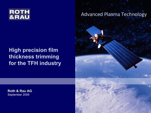
Advanced Plasma TechnologyHigh precision filmthickness trimmingfor the TFH industryRoth & Rau AGSeptember 2009
Product Overview<strong>IonScan</strong> Equipment for ultra-precise Surface Processing<strong>IonScan</strong> <strong>800</strong>• Wafer based processing insemiconductor industry• Applied for localized ion beamtrimming and figuring• Basically described in thispresentation2
Principle of <strong>IonScan</strong>Equipment Principle• Ion beam based surface processing capable for all thin film materials• Focused ion beam for locally controlled processing• Velocity controlled meander scan for local removal control3
Principle of <strong>IonScan</strong>Process Flow for Ion Beam Trimming20 nm 20 nm/s 40 msFrequency / Film thicknesserror of BAW waferEtch profile and focus of ionbeam (Material dependent)Calculation of residencetime dataWafer specific control data foraxis system1 nmProcess recipe data (Ion beamparameters, Cooling, Handling)Required input data:Velocity modulated waferscanFilm thickness error after ionbeam processing• Wafer specific thickness or frequency error file (Supplied by customer metrology)• Etch profile function from system calibration (Sheet film calibration data)• Material specific recipe data (beam settings, cooling, gas flow, …)4
Components & System LayoutSystem LayoutCluster Platform• Configurable cluster tool design with4 port handling unitProcess Chamber• Process chamber with high performanceaxis• Separate ion source housing for easysource access• Large front door for easy system accessSystem Control• Cluster and process module controller(Windows XP)• SECS/GEM host interface• Recipe and protocol database(MS SQL Server)Process module 1 Robot platform Cassette load-lock 1Ion sourceProcess module 2 Cassette load-lock 52
Components & System LayoutProcess Chamber• Rectangular chamber of <strong>800</strong> x <strong>800</strong> x 550 mm 3• Chamber and port dimensions capable for processing of up to 200 mm wafers• Chamber completely covered by sputter shields for maintenance• Separately accessible ion source housing for size and maintenance optimization• Turbo pumped (2400 l/s) viton sealed system (doors double sealed, differently pumped)with base pressure < 10-6 mbarIon Sourcex‐Axisy‐ AxisFaradayArrayz‐AxisTilt AxisWaferChuckHandlingPort6
Trimming PerformanceChallenge in Post CMP – Step Height Reduction<strong>IonScan</strong> <strong>800</strong> allows to overcome problems in CMP• Up-scaling for larger wafer areas causes homogeneity problems for CMP <strong>IonScan</strong> has no scaling problems• Polishing of different materials causes arbitrarily distributed step heights at interface tobe created <strong>IonScan</strong> is able to remove step functionsby adjusted process selectivity353025Rate [ nm/s ]201510500 10 20 30 40 50 60 70Incidence Angle [ deg ]InsulatorMetalSelectivity control by ion incident angle7
Trimming PerformanceStep Height Reduction by using High Selectivity353025Rate [ nm/s ]201510500 10 20 30 40 50 60 70Incidence Angle [ deg ]InsulatorMetalAl 2O 3NiFethickness variationover waferAl 2O 3NiFelocalized trimming8
Trimming PerformanceStep Height ReductionTop: Step heights reduction across of the wafer before (pre) and after (post) ion beam trimmingBottom left: Histogram graph of step height distributionBottom right: Trimming function of actual removal versus target removal9
Trimming PerformanceSmoothing by using Low Selectivity353025Rate [ nm/s ]201510500 10 20 30 40 50 60 70Incidence Angle [ deg ]InsulatorMetalAl 2O 3NiFethickness variationover waferAl 2O 3NiFelocalized trimming10
Trimming PerformanceAl 2 O 3 Trimming DemoTop: Thickness across the wafer before (pre) and after (post) ion beam trimmingBottom left: Histogram graph of thickness distributionBottom right: Trimming function of actual removal versus target removal11
Trimming PerformanceEtching to define Stepsthickness variationover waferMask Al 2O 3Maskdefined step highSubstratelocalizedtrimmingSubstrateEtching through different materials in one process step12
Thank you very muchfor your attention!Roth & Rau AGGewerbering 3OT Wüstenbrand09337 Hohenstein-ErnstthalGermanyRoth & Rau AGJuli 2006www.roth-rau.de