Implementation of Fast CRC Calculation
Implementation of Fast CRC Calculation
Implementation of Fast CRC Calculation

You also want an ePaper? Increase the reach of your titles
YUMPU automatically turns print PDFs into web optimized ePapers that Google loves.
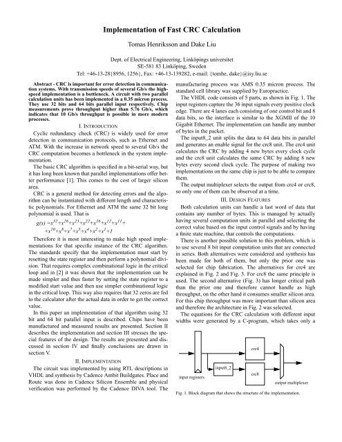
<strong>Implementation</strong> <strong>of</strong> <strong>Fast</strong> <strong>CRC</strong> <strong>Calculation</strong>Tomas Henriksson and Dake LiuDept. <strong>of</strong> Electrical Engineering, Linköpings universitetSE-581 83 Linköping, SwedenTel: +46-13-28{8956, 1256}, Fax: +46-13-139282, e-mail: {tomhe, dake}@isy.liu.seAbstract - <strong>CRC</strong> is important for error detection in communicationsystems. With transmission speeds <strong>of</strong> several Gb/s the highspeedimplementation is a bottleneck. A circuit with two parallelcalculation units has been implemented in a 0.35 micron process.They use 32 bits and 64 bits parallel input respectively. Chipmeasurements prove throughput higher than 5.76 Gb/s, whichindicates that 10 Gb/s throughput is possible in more modernprocesses.I. INTRODUCTIONCyclic redundancy check (<strong>CRC</strong>) is widely used for errordetection in communication protocols, such as Ethernet andATM. With the increase in network speed to several Gb/s the<strong>CRC</strong> computation becomes a bottleneck in the system implementation.The basic <strong>CRC</strong> algorithm is specified in a bit-serial way, butit has long been known that parallel implementations <strong>of</strong>fer betterperformance [1]. This comes to the cost <strong>of</strong> larger siliconarea.<strong>CRC</strong> is a general method for detecting errors and the algorithmcan be instantiated with different length and characteristicpolynomials. For Ethernet and ATM the same 32 bit longpolynomial is used. That isg(x) =x 32 +x 26 +x 23 +x 22 +x 16 +x 12 +x 11 ++x 10 +x 8 +x 7 +x 5 +x 4 +x 2 +x 1 +1Therefore it is most interesting to make high speed implementationsfor that specific instance <strong>of</strong> the <strong>CRC</strong> algorithm.The standards specify that the implementation must start byresetting the state register and then perform a polynomial division.That requires complex combinational logic in the criticalloop and in [2] it was shown that the implementation can bemade simpler and thus faster by setting the state register to amodified start value and then use simpler combinational logicin the critical loop. This way also requires that 32 zeros are fedto the calculator after the actual data in order to get the correctvalue.In this paper an implementation <strong>of</strong> that algorithm using 32bit and 64 bit parallel input is described. Chips have beenmanufactured and measured results are presented. Section IIdescribes the implementation and section III stresses the specialfeatures <strong>of</strong> the design. The results are presented and discussedin section IV and finally conclusions are drawn insection V.II. IMPLEMENTATIONThe circuit was implemented by using RTL descriptions inVHDL and synthesis by Cadence Ambit Buildgates. Place andRoute was done in Cadence Silicon Ensemble and physicalverification was performed by the Cadence DIVA tool. Themanufacturing process was AMS 0.35 micron process. Thestandard cell library was supplied by Europractice.The VHDL code consists <strong>of</strong> 5 parts, as shown in Fig. 1. Theinput registers capture the 36 input signals every positive clockedge. There are 4 lanes each consisting <strong>of</strong> one control bit and 8data bits, so the interface is similar to the XGMII <strong>of</strong> the 10Gigabit Ethernet. The implementation can handle any number<strong>of</strong> bytes in the packet.The input8_2 unit splits the data to 64 data bits in paralleland generates an enable signal for the crc8 unit. The crc4 unitcalculates the <strong>CRC</strong> by adding 4 new bytes every clock cycleand the crc8 unit calculates the same <strong>CRC</strong> by adding 8 newbytes every second clock cycle. The purpose <strong>of</strong> making twoimplementations on the same chip is just to be able to comparethem.The output multiplexer selects the output from crc4 or crc8,so only one <strong>of</strong> them can be observed at a time.III. DESIGN FEATURESBoth calculation units can handle a last word <strong>of</strong> data thatcontains any number <strong>of</strong> bytes. This is managed by actuallyhaving several computation units in parallel and selecting thecorrect value based on the input control signals and by havinga finite state machine, that controls the computations.There is another possible solution to this problem, which isto use several 8 bit input computation units that are connectedin series. Both alternatives were considered and synthesis hasbeen made for both <strong>of</strong> them, but only the prior one wasselected for chip fabrication. The alternatives for crc4 areexplained in Fig. 2 and Fig. 3. For crc8 the same principle isused. The second alternative (Fig. 3) has longer critical paththan the prior one and therefore cannot handle as highthroughput, on the other hand it consumes smaller silicon area.For this chip throughput was more important than silicon areaand therefore the architecture in Fig. 2 was selected.The equations for the <strong>CRC</strong> calculation with different inputwidths were generated by a C-program, which takes only ainput registersinput8_2crc4crc8output multiplexerFig. 1. Block diagram that shows the structure <strong>of</strong> the implementation.
lane 0 lane 1 lane 2 lane 3 ctrl8 bit <strong>CRC</strong> 16 bit <strong>CRC</strong> 24 bit <strong>CRC</strong> 32 bit <strong>CRC</strong>Fig. 2. The architecture selected for implementation8 bit <strong>CRC</strong>lane 0 lane 1 lane 2 lane 3Finitestatemachinectrl3 chips have been mounted on specially designed test boardsand measurements were conducted with Agilent 16700 logicanalysis system. The limitation in the testing was the testingequipment, which can only supply 180 MVectors/s. Theresults at supply voltage <strong>of</strong> 2.5 V are shown in table I. Because32 bits are processed every clock cycle a throughput <strong>of</strong>5.76 Gb/s is managed. All three chips operated at 180 MHzfor supply voltage from 2.2 V to 2.7 V. The crc8 circuit onchip #1 did, however, not work correctly.Why the chips did not work as fast at supply voltages above2.7 V is hard to explain. The crc4 on chip #1 operated correctlyat 130 MVectors/s at 3.3 V supply voltage, which is thenominal supply voltage for the process.Overall the manufactured chips worked better thanexpected. Static timing analysis estimated a maximumthroughput <strong>of</strong> 5.5 Gb/s for crc4 and 5.2 Gb/s for crc8, usingtypical process parameters in typical operating conditions.The reason why crc8 is estimated to support less throughputthan crc4 is that it uses an enable signal to control the operationand therefore has to use more complex flip-flops.8 bit <strong>CRC</strong>8 bit <strong>CRC</strong>8 bit <strong>CRC</strong>FinitestatemachineV. CONCLUSIONSA <strong>CRC</strong> chip has been designed and manufactured. Morethan 5.76 Gb/s throughput can be achieved in a 0.35 micronprocess. The results thereby indicate that 10 Gb/s throughputwill be possible in more modern processes.REFERENCES[1] T.-B. Pei and C. Zukowski, “High-speed parallel <strong>CRC</strong> circuits inVLSI”, IEEE Transactions on Communications, Vol. 40, pp. 653-657,April 1992.[2] R. J. Glaise and X. Jacquart, “<strong>Fast</strong> <strong>CRC</strong> <strong>Calculation</strong>”, Proceedings <strong>of</strong>IEEE International Conference on Computer Design: VLSI in Computers,pp. 602-605, 1993TABLE I MEASUREMENT RESULTSFig. 3. The alternative architecture, not selected for implementationpolynomial as the input. This was necessary since there are128 equations required for the crc8 unit. Actually units withup to 20 bytes input in parallel were also generated, but thesewere too complex to be implemented efficiently.In order to improve the throughput <strong>of</strong> the circuit, some techniqueswere used. First, flip-flops in the state register that havehigh fanout were cloned. Second, the most critical paths wereidentified and logic was pushed over the register boundary torelax the critical paths. This, <strong>of</strong> course, had to be compensatedfor at the output.The observability <strong>of</strong> the circuit is further improved by havingthe possibility to select internal states with the output multiplexer.This is not shown in Fig. 1, but the output multiplexerhas actually 4 inputs <strong>of</strong> 32 bits each, 2 <strong>of</strong> those are the <strong>CRC</strong>values from crc4 and crc8 respectively. The other 2 are builtup by internal states which can be used for testing purposes.IV. RESULTS AND DISCUSSIONThe total chip implemented in 0.35 micron technology uses7.73 mm 2 silicon area, see Fig. 4. It has 84 pads and is padlimited. The area <strong>of</strong> the core is 2.87 mm 2 .Chip # crc4 throughput crc8 throughput1 5.76 Gb/s Failure2 5.76 Gb/s 5.76 Gb/s3 5.76 Gb/s 5.76 Gb/sFig. 4. Chip photo. The chip area is 7.73 mm 2 .