The Effects of Increasing the Aspect Ratio of GaAs ... - CS Mantech
The Effects of Increasing the Aspect Ratio of GaAs ... - CS Mantech
The Effects of Increasing the Aspect Ratio of GaAs ... - CS Mantech

You also want an ePaper? Increase the reach of your titles
YUMPU automatically turns print PDFs into web optimized ePapers that Google loves.
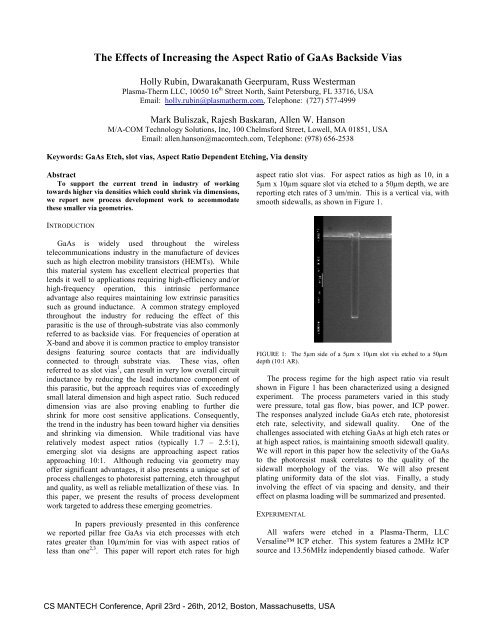
<strong>The</strong> <strong>Effects</strong> <strong>of</strong> <strong>Increasing</strong> <strong>the</strong> <strong>Aspect</strong> <strong>Ratio</strong> <strong>of</strong> <strong>GaAs</strong> Backside ViasHolly Rubin, Dwarakanath Geerpuram, Russ WestermanPlasma-<strong>The</strong>rm LLC, 10050 16 th Street North, Saint Petersburg, FL 33716, USAEmail: holly.rubin@plasma<strong>the</strong>rm.com, Telephone: (727) 577-4999Mark Buliszak, Rajesh Baskaran, Allen W. HansonM/A-COM Technology Solutions, Inc, 100 Chelmsford Street, Lowell, MA 01851, USAEmail: allen.hanson@macomtech.com, Telephone: (978) 656-2538Keywords: <strong>GaAs</strong> Etch, slot vias, <strong>Aspect</strong> <strong>Ratio</strong> Dependent Etching, Via densityAbstractTo support <strong>the</strong> current trend in industry <strong>of</strong> workingtowards higher via densities which could shrink via dimensions,we report new process development work to accommodate<strong>the</strong>se smaller via geometries.aspect ratio slot vias. For aspect ratios as high as 10, in a5µm x 10µm square slot via etched to a 50µm depth, we arereporting etch rates <strong>of</strong> 3 um/min. This is a vertical via, withsmooth sidewalls, as shown in Figure 1.INTRODUCTION<strong>GaAs</strong> is widely used throughout <strong>the</strong> wirelesstelecommunications industry in <strong>the</strong> manufacture <strong>of</strong> devicessuch as high electron mobility transistors (HEMTs). Whilethis material system has excellent electrical properties thatlends it well to applications requiring high-efficiency and/orhigh-frequency operation, this intrinsic performanceadvantage also requires maintaining low extrinsic parasiticssuch as ground inductance. A common strategy employedthroughout <strong>the</strong> industry for reducing <strong>the</strong> effect <strong>of</strong> thisparasitic is <strong>the</strong> use <strong>of</strong> through-substrate vias also commonlyreferred to as backside vias. For frequencies <strong>of</strong> operation atX-band and above it is common practice to employ transistordesigns featuring source contacts that are individuallyconnected to through substrate vias. <strong>The</strong>se vias, <strong>of</strong>tenreferred to as slot vias 1 , can result in very low overall circuitinductance by reducing <strong>the</strong> lead inductance component <strong>of</strong>this parasitic, but <strong>the</strong> approach requires vias <strong>of</strong> exceedinglysmall lateral dimension and high aspect ratio. Such reduceddimension vias are also proving enabling to fur<strong>the</strong>r dieshrink for more cost sensitive applications. Consequently,<strong>the</strong> trend in <strong>the</strong> industry has been toward higher via densitiesand shrinking via dimension. While traditional vias haverelatively modest aspect ratios (typically 1.7 – 2.5:1),emerging slot via designs are approaching aspect ratiosapproaching 10:1. Although reducing via geometry may<strong>of</strong>fer significant advantages, it also presents a unique set <strong>of</strong>process challenges to photoresist patterning, etch throughputand quality, as well as reliable metallization <strong>of</strong> <strong>the</strong>se vias. Inthis paper, we present <strong>the</strong> results <strong>of</strong> process developmentwork targeted to address <strong>the</strong>se emerging geometries.In papers previously presented in this conferencewe reported pillar free <strong>GaAs</strong> via etch processes with etchrates greater than 10µm/min for vias with aspect ratios <strong>of</strong>less than one 2,3 . This paper will report etch rates for highFIGURE 1: <strong>The</strong> 5µm side <strong>of</strong> a 5µm x 10µm slot via etched to a 50µmdepth (10:1 AR).<strong>The</strong> process regime for <strong>the</strong> high aspect ratio via resultshown in Figure 1 has been characterized using a designedexperiment. <strong>The</strong> process parameters varied in this studywere pressure, total gas flow, bias power, and ICP power.<strong>The</strong> responses analyzed include <strong>GaAs</strong> etch rate, photoresistetch rate, selectivity, and sidewall quality. One <strong>of</strong> <strong>the</strong>challenges associated with etching <strong>GaAs</strong> at high etch rates orat high aspect ratios, is maintaining smooth sidewall quality.We will report in this paper how <strong>the</strong> selectivity <strong>of</strong> <strong>the</strong> <strong>GaAs</strong>to <strong>the</strong> photoresist mask correlates to <strong>the</strong> quality <strong>of</strong> <strong>the</strong>sidewall morphology <strong>of</strong> <strong>the</strong> vias. We will also presentplating uniformity data <strong>of</strong> <strong>the</strong> slot vias. Finally, a studyinvolving <strong>the</strong> effect <strong>of</strong> via spacing and density, and <strong>the</strong>ireffect on plasma loading will be summarized and presented.EXPERIMENTALAll wafers were etched in a Plasma-<strong>The</strong>rm, LLCVersaline ICP etcher. This system features a 2MHz ICPsource and 13.56MHz independently biased cathode. Wafer<strong>CS</strong> MANTECH Conference, April 23rd - 26th, 2012, Boston, Massachusetts, USA
temperature was controlled by electrostatically clamping <strong>the</strong>wafer to a cooled cathode with helium backside cooling.<strong>The</strong> substrates used in <strong>the</strong>se experiments were 100mm,full thickness, mechanical <strong>GaAs</strong> wafers patterned with aphotoresist mask. <strong>The</strong> effective open area <strong>of</strong> <strong>GaAs</strong> due to<strong>the</strong> vias was less than 10%.All <strong>GaAs</strong> etch depth measurements were taken from viasat <strong>the</strong> center <strong>of</strong> <strong>the</strong> wafers. <strong>The</strong>se measurements wereperformed using an Amray Scanning Electron Microscopemodel 1830. A Nanometrics NanoSpec model 6100spectroscopic reflectometer was used to measure <strong>the</strong>photoresist thickness. Twenty-five sites on each wafer weremeasured before and after etch, with an edge exclusion <strong>of</strong>6mm. An average <strong>of</strong> <strong>the</strong> 25 point measurement was used in<strong>the</strong> calculations <strong>of</strong> photoresist etch rate and selectivity.<strong>The</strong> DOE to characterize <strong>the</strong> process space was setup andanalyzed using Design Expert s<strong>of</strong>tware from Stat-Ease, Inc.An irregular fraction design was utilized to construct <strong>the</strong>experiments covering 4 factors in 12 experiments with 3repeats <strong>of</strong> <strong>the</strong> center point for 15 total experiments. Anirregular fraction allows <strong>the</strong> estimation <strong>of</strong> <strong>the</strong> main effects aswell as 2 factor interactions. <strong>The</strong> effects <strong>of</strong> <strong>the</strong>se factorswere characterized through <strong>the</strong> four captured responses:<strong>GaAs</strong> etch rate, photoresist etch rate, selectivity, and viasidewall quality. Total etch time, process temperature, andhardware configuration were held constant throughout <strong>the</strong>seexperiments.<strong>The</strong> sidewall quality <strong>of</strong> <strong>the</strong> vias was evaluated after aphotoresist strip in an acetone bath. Cross-sectional SEMimages <strong>of</strong> <strong>the</strong>se vias were presented to several engineers fora numerical evaluation <strong>of</strong> <strong>the</strong> quality. <strong>The</strong> average <strong>of</strong> <strong>the</strong>seratings was used as <strong>the</strong> response.RESULTS AND DISCUSSIONReducing <strong>the</strong> total flow at constant pressure or reducing <strong>the</strong>total flow at higher pressures leads to longer residence timesfor <strong>the</strong> reactants. Longer residence times give <strong>the</strong> availablereactants more time within <strong>the</strong> system to react with <strong>the</strong> etchsurface. <strong>The</strong> residence times in this DOE ranged from 0.45seconds to 2 seconds.Photoresist etch rate increases with increasing bias andICP powers. This can be attributed to an increase in powerdensity at <strong>the</strong> wafer. <strong>The</strong> increase in photoresist etch ratedue to Cl 2 gas flow can be attributed to a higherconcentration <strong>of</strong> Cl available to react with <strong>the</strong> photoresist.<strong>The</strong> highest photoresist etch rates occurred at <strong>the</strong> lowestpressures, highest Cl 2 flows, and highest powersinvestigated. Figure 2 shows <strong>the</strong> dependence <strong>of</strong> photoresistetch rate on Cl 2 flow and pressure at a given power level.Consequently, selectivity decreased with increasing powersdue to <strong>the</strong> photoresist etching considerably faster at higherpowers. Also, <strong>the</strong>re is a direct relationship between pressureand selectivity. As pressure increases, so does selectivity.A summary <strong>of</strong> <strong>the</strong> rating system used to evaluate <strong>the</strong>sidewall quality <strong>of</strong> <strong>the</strong> vias is described with Figure 3. Aninteraction <strong>of</strong> factors was observed when looking at <strong>the</strong>response <strong>of</strong> sidewall quality <strong>of</strong> <strong>the</strong> vias. At higher Cl 2 flows,sidewall quality decreases with increasing pressure. But atlower Cl 2 flows, sidewall morphology is smooth andindependent <strong>of</strong> pressure changes in <strong>the</strong> factor rangeinvestigated, as shown in Figure 4. This could be attributedto a reactant limited scenario at <strong>the</strong> lower flows.Figure 5 illustrates <strong>the</strong> correlation drawn betweenselectivity and <strong>the</strong> quality <strong>of</strong> <strong>the</strong> sidewall morphology <strong>of</strong> <strong>the</strong>vias studied. It was found that <strong>the</strong> smoo<strong>the</strong>r sidewallmorphology <strong>of</strong> <strong>the</strong> vias occurred at <strong>the</strong> lower selectivities.This would indicate that more photoresist-based polymer isbeing produced at <strong>the</strong> higher photoresist etch rates, to betterprotect <strong>the</strong> sidewalls <strong>of</strong> <strong>the</strong> vias.A) Designed ExperimentIn Table I, <strong>the</strong> general response trends from <strong>the</strong> DOE aresummarized. <strong>The</strong> arrows indicate <strong>the</strong> directional change in<strong>the</strong> response resulting from an increase in <strong>the</strong> listed processfactor.TABLE IIGENERAL RESPONSE TRENDS FROM DOEResponsesFactors<strong>GaAs</strong>EtchRatePhotoresistEtchRateSelectivity(<strong>GaAs</strong>:PR)SidewallQualityPressure ↑ ↑ ↓ ↑ ↓Cl 2 Flow ↑ ↑ ↑ ↓Bias Power ↑ ↑ ↓ICP Power ↑ ↑ ↓Increases in <strong>GaAs</strong> etch rate are shown to be directlyrelated to increases in pressure and total Cl 2 gas flow.FIGURE 2: Interaction effects <strong>of</strong> pressure and Cl 2 flow on photoresist etchrate (Å/min). High photoresist etch rates (Å/min) occur at low pressuresand high Cl 2 flows.<strong>CS</strong> MANTECH Conference, April 23rd - 26th, 2012, Boston, Massachusetts, USA
B) <strong>Aspect</strong> <strong>Ratio</strong> Dependent Etching <strong>of</strong> Slot ViasWe are also presenting <strong>the</strong> aspect ratio dependent etchrate data for slot vias. This topic has been studied in <strong>the</strong> pastfor a RIE only process 4 . This work presents an extension <strong>of</strong>that curve using an ICP process.A B CFIGURE 3: Examples <strong>of</strong> via images used in <strong>the</strong> sidewall quality evaluation.<strong>The</strong> engineers surveyed assessed only <strong>the</strong> sidewall morphology. <strong>The</strong>y weregiven <strong>the</strong> scale <strong>of</strong> 1 representing many sidewall voids and 10 representing avia with very smooth sidewalls. <strong>The</strong> average rating <strong>of</strong> via A was 2.5, via Bwas 4.5, and via C was 10.If A defines <strong>the</strong> radius <strong>of</strong> <strong>the</strong> via in <strong>the</strong> x-direction and Bdefines <strong>the</strong> radius <strong>of</strong> <strong>the</strong> via in <strong>the</strong> y-direction. When A=B,<strong>the</strong> vias are circular and <strong>the</strong> aspect ratio (AR) is defined tobe <strong>the</strong> ratio <strong>of</strong> <strong>the</strong> etch depth (D) to <strong>the</strong> diameter <strong>of</strong> <strong>the</strong> via(2*A = 2*B). For slot vias, when A < B, <strong>the</strong>n <strong>the</strong> aspectratio (AR) is defined as AR = D / 2*A.<strong>The</strong> center point process <strong>of</strong> <strong>the</strong> DOE was used togenerate <strong>the</strong> data in <strong>the</strong> curve presented in Figure 7. <strong>The</strong>etch rate data is a time based average. <strong>The</strong> same processwas used and <strong>the</strong> etch depth was measured at 2 minuteintervals <strong>of</strong> <strong>the</strong> etch. This was done to assess how fast <strong>the</strong>etch depth increased over time. <strong>The</strong>se vias were all grassfree and showed smooth sidewalls. Five different slot viasizes were measured and plotted on <strong>the</strong> curve, ranging from20 x 25µm vias to 20 x 5µm vias. We are reporting <strong>the</strong>capability to etch 10 x 5µm slot vias to more than a 50µmetch depth with smooth sidewalls, as seen in Figure 1. Thisgives a greater than 10:1 aspect ratio via etched at more than3µm/min.BADFIGURE 4: Interaction effects <strong>of</strong> pressure and Cl 2 flow on sidewall quality.Sidewall quality scale with a 1 represents a via with a lot <strong>of</strong> sidewall voidsand a rating <strong>of</strong> 10 represents a via with very smooth sidewalls. At higherCl 2 flows, sidewall quality decreases with increasing pressure. At lower Cl 2flows, sidewall quality is independent <strong>of</strong> pressure.FIGURE 6: Illustration depicting slot via dimensions, where A is <strong>the</strong> radiusin <strong>the</strong> x-direction, B is <strong>the</strong> radius in <strong>the</strong> y-direction and D is <strong>the</strong> total etchdepth.FIGURE 5: Correlation <strong>of</strong> Selectivity to Sidewall Quality, <strong>the</strong> higher <strong>the</strong>selectivity <strong>the</strong> lower <strong>the</strong> sidewall quality.FIGURE 7: Time averaged etch rate as a function <strong>of</strong> aspect ratio for slotvias, from 20x25µm to 20x5µm slot vias.<strong>CS</strong> MANTECH Conference, April 23rd - 26th, 2012, Boston, Massachusetts, USA
C) Plating UniformityAlso presented are <strong>the</strong> results <strong>of</strong> a test reticle created for<strong>the</strong>se studies that features vias <strong>of</strong> various size and densitythat was used to quantify etch and plating systeminteractions. A series <strong>of</strong> via sizes ranging from 15x5µm to15x30µm from <strong>the</strong> test reticle are shown in Figure 8A.Figures 8B and 8C illustrate <strong>the</strong> extent <strong>of</strong> plated taperpresent in <strong>the</strong> process – metallization thickness was found toconsistently maintain approximately 85% <strong>of</strong> its nominalvalue from back to front. Overall, excellent platinguniformity was obtained for all via geometries in this series.A B CFIGURE 8: Figure 8A shows a series <strong>of</strong> via sizes ranging from 15x5µm to15x30µm. Figure 8B shows <strong>the</strong> gold on <strong>the</strong> sidewall at <strong>the</strong> top <strong>of</strong> <strong>the</strong> via tobe 2.8µm thick. Figure 8C shows <strong>the</strong> gold on <strong>the</strong> sidewall at <strong>the</strong> bottom <strong>of</strong><strong>the</strong> via to be 2.4 µm thick.D) Study <strong>of</strong> Via Spacing and DensityA study involving <strong>the</strong> effect <strong>of</strong> via spacing and densityand <strong>the</strong>ir effect on plasma loading was also conducted. Aseries <strong>of</strong> 10 x 20 µm Vias with varying pitch in X and Ydirections in 12 distinct pads was created from a sparse viadensity <strong>of</strong> 80 vias, to a high density <strong>of</strong> 240 vias.<strong>The</strong> center-point <strong>of</strong> <strong>the</strong> triplicate run (from DOE) waferwas selected for analysis. <strong>The</strong> variations in diameter, anddepth <strong>of</strong> <strong>the</strong> vias etched in <strong>the</strong> various X and Y pitches anddensities from 80 vias (<strong>the</strong> most sparsely populated array) to240 vias (most densely populated array) was remarkably lowat 1 sigma