CIICT 2009 Proceedings
CIICT 2009 Proceedings
CIICT 2009 Proceedings
- No tags were found...

Create successful ePaper yourself
Turn your PDF publications into a flip-book with our unique Google optimized e-Paper software.
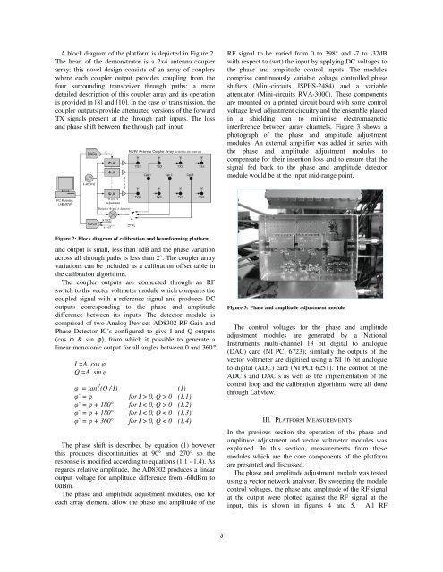
A block diagram of the platform is depicted in Figure 2.The heart of the demonstrator is a 2x4 antenna couplerarray; this novel design consists of an array of couplerswhere each coupler output provides coupling from thefour surrounding transceiver through paths; a moredetailed description of this coupler array and its operationis provided in [8] and [10]. In the case of transmission, thecoupler outputs provide attenuated versions of the forwardTX signals present at the through path inputs. The lossand phase shift between the through path inputRF signal to be varied from 0 to 398° and -7 to -32dBwith respect to (wrt) the input by applying DC voltages tothe phase and amplitude control inputs. The modulescomprise continuously variable voltage controlled phaseshifters (Mini-circuits JSPHS-2484) and a variableattenuator (Mini-circuits RVA-3000). These componentsare mounted on a printed circuit board with some controlvoltage level adjustment circuitry and the ensemble placedin a shielding can to minimise electromagneticinterference between array channels. Figure 3 shows aphotograph of the phase and amplitude adjustmentmodules. An external amplifier was added in series withthe phase and amplitude adjustment modules tocompensate for their insertion loss and to ensure that thesignal fed back to the phase and amplitude detectormodule would be at the input mid-range point.Figure 2: Block diagram of calibration and beamforming platformand output is small, less than 1dB and the phase variationacross all through paths is less than 2°. The coupler arrayvariations can be included as a calibration offset table inthe calibration algorithms.The coupler outputs are connected through an RFswitch to the vector voltmeter module which compares thecoupled signal with a reference signal and produces DCoutputs corresponding to the phase and amplitudedifference between its inputs. The detector module iscomprised of two Analog Devices AD8302 RF Gain andPhase Detector IC’s configured to give I and Q outputs(cos φ & sin φ), from which it possible to generate alinear monotonic output for all angles between 0 and 360°.I =A. cos φQ =A. sin φφ = tan -1 (Q / I) (1)φ` = φ for I > 0, Q > 0 (1.1)φ` = φ + 180° for I < 0, Q > 0 (1.2)φ` = φ + 180° for I < 0, Q < 0 (1.3)φ` = φ + 360° for I > 0, Q < 0 (1.4)The phase shift is described by equation (1) howeverthis produces discontinuities at 90° and 270° so theresponse is modified according to equations (1.1 - 1.4). Asregards relative amplitude, the AD8302 produces a linearoutput voltage for amplitude difference from -60dBm to0dBm.The phase and amplitude adjustment modules, one foreach array element, allow the phase and amplitude of theFigure 3: Phase and amplitude adjustment moduleThe control voltages for the phase and amplitudeadjustment modules are generated by a NationalInstruments multi-channel 13 bit digital to analogue(DAC) card (NI PCI 6723); similarly the outputs of thevector voltmeter are digitised using a NI 16 bit analogueto digital (ADC) card (NI PCI 6251). The control of theADC’s and DAC’s as well as the implementation of thecontrol loop and the calibration algorithms were all donethrough Labview.III. PLATFORM MEASUREMENTSIn the previous section the operation of the phase andamplitude adjustment and vector voltmeter modules wasexplained. In this section, measurements from thesemodules which are the core components of the platformare presented and discussed.The phase and amplitude adjustment module was testedusing a vector network analyser. By sweeping the modulecontrol voltages, the phase and amplitude of the RF signalat the output were plotted against the RF signal at theinput, this is shown in figures 4 and 5. All RF3