

Building radio systems from digital parts - Politecnico di Torino
Building radio systems from digital parts - Politecnico di Torino
Building radio systems from digital parts - Politecnico di Torino

You also want an ePaper? Increase the reach of your titles
YUMPU automatically turns print PDFs into web optimized ePapers that Google loves.
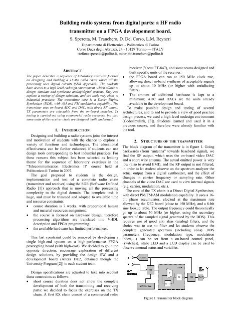
<strong>Buil<strong>di</strong>ng</strong> <strong>ra<strong>di</strong>o</strong> <strong>systems</strong> <strong>from</strong> <strong><strong>di</strong>gital</strong> <strong>parts</strong>: a HF <strong>ra<strong>di</strong>o</strong>transmitter on a FPGA developement board.S. Speretta, M. Tranchero, D. Del Corso, L.M. ReyneriDipartimento <strong>di</strong> Elettronica - <strong>Politecnico</strong> <strong>di</strong> <strong>Torino</strong>Corso Duca degli Abruzzi, 24 - 10129 <strong>Torino</strong> — ITALYstefano.speretta@polito.it, maurizio.tranchero@polito.itABSTRACTThe paper describes a sequence of laboratory exercises focusedon designing and buil<strong>di</strong>ng a TX-RX <strong>ra<strong>di</strong>o</strong> chain where all theprocessing uses <strong><strong>di</strong>gital</strong> circuits (SDR approach). The studentshave access to a high-level codesign environment, which allows todesign, simulate and synthesize analog/<strong><strong>di</strong>gital</strong> <strong>systems</strong>. They canexplore a variety of design solutions, and use tools very close toindustrial practices. The transmitter core is a Direct DigitalSynthesizer (DDS), with AM and FM modulation capability. Thetransmitter uses on-board ADC and DAC, with <strong>di</strong>rect RF output.TX parameters are selectable <strong>from</strong> the on-board switches. Txtesting is carried out using commercial <strong>ra<strong>di</strong>o</strong> receivers, but alsosome units of the receiver chain are designed, built, and tested.1. INTRODUCTIONDesigning and buil<strong>di</strong>ng a <strong>ra<strong>di</strong>o</strong> <strong>systems</strong> joins the interestand motivation of students with the chance to explore avariety of functions and technologies. The educationaleffectiveness can be further enhanced if students can usedesign tools correspon<strong>di</strong>ng to best industrial practices. Forthese reasons this subject has been selected as lea<strong>di</strong>ngtheme for the sequence of laboratory exercises in the"Telecommunication Electronics II" course held at<strong>Politecnico</strong> <strong>di</strong> <strong>Torino</strong> in 2007.The goal proposed to students is the design,implementation and test of a complete <strong>ra<strong>di</strong>o</strong> chain(transmitter and receiver) using the SDR (Software DefinedRa<strong>di</strong>o [1]) approach that is moving all the processingcomplexity to the <strong><strong>di</strong>gital</strong> domain. The complete task ishuge, and must be trimmed and adapted to available timeand resource constraints:• course duration is 7 weeks, with proportional humanand material resources assignment.• the course is focused on hardware design, thereforeprocessing algorithms are translated into VHDLdescription and FPGA programming.• the available hardware has limited performances.This last constraint could be removed by developing asingle high-end system on a high-performance FPGAprototyping board (with high-cost). We decided to go in theopposite <strong>di</strong>rection: encourage exploration of <strong>di</strong>fferentdesign solutions, by provi<strong>di</strong>ng the design SW and adevelopment board (Altera DE2, obtained though theUniversity Program [2]) to each student team.Design specifications are adjusted to take into accountthese constraints as follows:• short course duration does not allow the completedevelopment of both the transmitting and receiving<strong>parts</strong>: we decided to focus the exercises on the TXchain. A first RX chain consist of a commercial <strong>ra<strong>di</strong>o</strong>receiver (Yaesu FT-847), and some teams designed andbuilt specific units of the receiver.• the FPGA board can run at 150 MHz clock rate,allowing <strong>di</strong>rect in-band synthesis of acceptable signalsup to about 10 MHz (or higher with antialiasingfilters).• The amount of ad<strong>di</strong>tional hardware is kept to aminimum; ADC and DACs are the units alreadyavailable in the development board.To make possible design and testing of severalarchitectures, and to and to provide a view of good practicedesign process, we used a high-level codesign environment(Codesimulink, [3]). Students learned and used it in aprevious course, and therefore were already familiar withthe tool.2. STRUCTURE OF THE TRANSMITTERThe block <strong>di</strong>agram of the transmitter is in figure 1. Goingbackwards (<strong>from</strong> “antenna” towards baseband signal), wefind the RF output, which uses the on-board video DACand a short wire antenna. The actual emitted power is verylow (also to avoid EMI), and the RF output is not filtered,in order to let student observe on the spectrum analyzer theactual output <strong>from</strong> a <strong><strong>di</strong>gital</strong> synthesizer, and the effect ofchanges in carrier frequency or sampling rate. Otherchannels of the video DAC are used to view internal signals(e.g. carrier, modulation, etc.).The core of the TX chain is a Direct Digital Synthesizer,with <strong>di</strong>rect PM/FM/AM modulation capability. It uses a 16-bit phase accumulator, clocked at the maximum rateallowed by the DE2 board (close to 150 MHz), and a 8-bitsine lookup table. The output frequency could theoreticallygo up to about 50 MHz (or higher, using the secondaryspectra of the sampled signal generated by the DDS). Thisrequires use of good anti alias (analog) filters, and thechoice was to use no filter and let students observe thecomplete generated spectrum (inclu<strong>di</strong>ng alias). DDSparameters (frequency, modulation type, modulationindex,…) can be set <strong>from</strong> a on-board control panel,(switches), while LED and a LCD <strong>di</strong>splay can be used toobserve internal status and variables.Figure 1: transmitter block <strong>di</strong>agram
The baseband signal (modulation) is fed to the systemthrough the on-board au<strong>di</strong>o CODEC (A), or through <strong>di</strong>rect<strong><strong>di</strong>gital</strong> input lines (D).3. THE DESIGN TOOLThe development is carried out using an high-level codesignenvironment internally developed at <strong>Politecnico</strong> <strong>di</strong><strong>Torino</strong> (CodeSimulink). It allows to design, simulate andsynthesize VHDL code for any mixed analog/<strong><strong>di</strong>gital</strong>system, using an extension of Simulink (The Mathworks).The developed model can be simulated and validated withinthe MATLAB environment, with the added capability tohandle analog units. CodeSimulink dramatically reduces thedevelopment phase by <strong>di</strong>rect generation of VHDL or Ccodes, for implementation on FPGA or DSP, and allowssimulation of the whole system in an integratedenvironment. Cost and performance of <strong>di</strong>fferentanalog/<strong><strong>di</strong>gital</strong> or HW/SW tradeoffs, or various architecturesfor <strong><strong>di</strong>gital</strong> units can be easily explored, and various systemimplementations can be evaluated before going down to thedetailed design.Since the course is focused on <strong><strong>di</strong>gital</strong> hardware design,we used the VHDL output for FPGA programming. WithDSPs precision is usually not an issue, (floating pointvariable handled <strong>di</strong>rectly by the HW), while FPGA requireoptimization of resources and power, that means carefulevaluation of the number of bits to be used on each step ofthe processing. The Codesimulink developmentenvironment makes possible to mo<strong>di</strong>fy the variablerepresentation on each unit, and speeds up the designoptimization process.As the design is completed, a compiler translates thebuil<strong>di</strong>ng blocks in VHDL using ad hoc developed libraries.Low-level implementation details (like fixed pointarithmetic or pipeline levels) are then introduced in a highlevellanguage, and their influence on system performancescan be <strong>di</strong>rectly evaluated. Synthesis is performed usingcommercial tools for both ASIC and FPGA like AlteraQuartus, Xilinx ISE or Mentor Graphics LeonardoSpectrum, which generate the code to be downloaded onthe development board. This approach allows the student tofocus only on the high-level algorithm and explore <strong>di</strong>fferentsolutions, with an "automated" implementation, lea<strong>di</strong>ng to ashort development time.4. DESIGN RESULTSThe transmitter uses the DE2 development board <strong>from</strong>Altera, based on a Cyclone II FPGA, using local DAC andADC, without external hardware. The high speed tripleDAC (SVGA video output), is used for <strong>di</strong>rect synthesis ofthe RF modulated signal, and the au<strong>di</strong>o CODEC is used forsignal acquisition <strong>from</strong> external sources (MP3 players wereused for the lab experiments). Two HF <strong>ra<strong>di</strong>o</strong>s were used astest receivers: a Yaesu FT-847 (classic architecture) and aSW <strong>ra<strong>di</strong>o</strong> based on a downconverter which sends <strong>di</strong>gitizedIF I/Q components to a PC through a USB interface(CiaoRa<strong>di</strong>o [4]). An example of spectrum of RF signal withAM modulation is in figure 3 (due to the low oversamplingrate, the <strong>di</strong>agram includes the first alias).Some teams developed also units of the receiver(demodulators). Due to lack of high speed ADC, the "RF"input is the sequence of <strong><strong>di</strong>gital</strong> samples generated by thetransmitter. Half-wave and full-wave envelope decoder, anda PLL-based synchronous receiver are used for AM and FMdemodulation. The PLL is fully <strong><strong>di</strong>gital</strong> and exploits theFPGA embedded high-speed multipliers, thus achieving anoperating speed of 150 MHz. The channel transfer functioncan be evaluated by comparing input modulation anddemodulated output signal (rebuilt by the au<strong>di</strong>o codec).5. ACKNOWLEDGMENTThe boards used by students in the lab were donatedthrough the Altera University Program.REFERENCES[1] A. Abi<strong>di</strong>, “The path to the software-defined <strong>ra<strong>di</strong>o</strong> receiver”IEEE J. Solid State Circuits, vol. 42, pp. 954-966, May 2007.[2] Altera. De2 board documentation. [Online]. Available:http://www.altera.com/education/univ[3] E. Bellei, E. Bussolino, F. Gregoretti, L. Mari, F. Renga andL.M. Reyneri, “Simulink-based codesing and cosimulation of acommon-rail injector test bench”, Journal on Computer, Systemsand Circuits, Volume 12, pp. 171-202, 2003.[4] Computer Interface Au<strong>di</strong>o Output Ra<strong>di</strong>o (CIAO Ra<strong>di</strong>o):http://www.comsistel.com/drm.htmFigure 2: transmitter CodeSimulink block


